JP2014116604A - Light emitting device - Google Patents
Light emitting device Download PDFInfo
- Publication number
- JP2014116604A JP2014116604A JP2013251766A JP2013251766A JP2014116604A JP 2014116604 A JP2014116604 A JP 2014116604A JP 2013251766 A JP2013251766 A JP 2013251766A JP 2013251766 A JP2013251766 A JP 2013251766A JP 2014116604 A JP2014116604 A JP 2014116604A
- Authority
- JP
- Japan
- Prior art keywords
- light emitting
- layer
- electrode
- disposed
- current blocking
- Prior art date
- Legal status (The legal status is an assumption and is not a legal conclusion. Google has not performed a legal analysis and makes no representation as to the accuracy of the status listed.)
- Pending
Links
Images


Classifications
-
- H—ELECTRICITY
- H01—ELECTRIC ELEMENTS
- H01L—SEMICONDUCTOR DEVICES NOT COVERED BY CLASS H10
- H01L27/00—Devices consisting of a plurality of semiconductor or other solid-state components formed in or on a common substrate
- H01L27/15—Devices consisting of a plurality of semiconductor or other solid-state components formed in or on a common substrate including semiconductor components with at least one potential-jump barrier or surface barrier specially adapted for light emission
- H01L27/153—Devices consisting of a plurality of semiconductor or other solid-state components formed in or on a common substrate including semiconductor components with at least one potential-jump barrier or surface barrier specially adapted for light emission in a repetitive configuration, e.g. LED bars
- H01L27/156—Devices consisting of a plurality of semiconductor or other solid-state components formed in or on a common substrate including semiconductor components with at least one potential-jump barrier or surface barrier specially adapted for light emission in a repetitive configuration, e.g. LED bars two-dimensional arrays
-
- H—ELECTRICITY
- H01—ELECTRIC ELEMENTS
- H01L—SEMICONDUCTOR DEVICES NOT COVERED BY CLASS H10
- H01L27/00—Devices consisting of a plurality of semiconductor or other solid-state components formed in or on a common substrate
- H01L27/15—Devices consisting of a plurality of semiconductor or other solid-state components formed in or on a common substrate including semiconductor components with at least one potential-jump barrier or surface barrier specially adapted for light emission
-
- H—ELECTRICITY
- H01—ELECTRIC ELEMENTS
- H01L—SEMICONDUCTOR DEVICES NOT COVERED BY CLASS H10
- H01L33/00—Semiconductor devices with at least one potential-jump barrier or surface barrier specially adapted for light emission; Processes or apparatus specially adapted for the manufacture or treatment thereof or of parts thereof; Details thereof
- H01L33/02—Semiconductor devices with at least one potential-jump barrier or surface barrier specially adapted for light emission; Processes or apparatus specially adapted for the manufacture or treatment thereof or of parts thereof; Details thereof characterised by the semiconductor bodies
- H01L33/10—Semiconductor devices with at least one potential-jump barrier or surface barrier specially adapted for light emission; Processes or apparatus specially adapted for the manufacture or treatment thereof or of parts thereof; Details thereof characterised by the semiconductor bodies with a light reflecting structure, e.g. semiconductor Bragg reflector
-
- H—ELECTRICITY
- H01—ELECTRIC ELEMENTS
- H01L—SEMICONDUCTOR DEVICES NOT COVERED BY CLASS H10
- H01L33/00—Semiconductor devices with at least one potential-jump barrier or surface barrier specially adapted for light emission; Processes or apparatus specially adapted for the manufacture or treatment thereof or of parts thereof; Details thereof
- H01L33/02—Semiconductor devices with at least one potential-jump barrier or surface barrier specially adapted for light emission; Processes or apparatus specially adapted for the manufacture or treatment thereof or of parts thereof; Details thereof characterised by the semiconductor bodies
- H01L33/14—Semiconductor devices with at least one potential-jump barrier or surface barrier specially adapted for light emission; Processes or apparatus specially adapted for the manufacture or treatment thereof or of parts thereof; Details thereof characterised by the semiconductor bodies with a carrier transport control structure, e.g. highly-doped semiconductor layer or current-blocking structure
- H01L33/145—Semiconductor devices with at least one potential-jump barrier or surface barrier specially adapted for light emission; Processes or apparatus specially adapted for the manufacture or treatment thereof or of parts thereof; Details thereof characterised by the semiconductor bodies with a carrier transport control structure, e.g. highly-doped semiconductor layer or current-blocking structure with a current-blocking structure
-
- H—ELECTRICITY
- H01—ELECTRIC ELEMENTS
- H01L—SEMICONDUCTOR DEVICES NOT COVERED BY CLASS H10
- H01L33/00—Semiconductor devices with at least one potential-jump barrier or surface barrier specially adapted for light emission; Processes or apparatus specially adapted for the manufacture or treatment thereof or of parts thereof; Details thereof
- H01L33/36—Semiconductor devices with at least one potential-jump barrier or surface barrier specially adapted for light emission; Processes or apparatus specially adapted for the manufacture or treatment thereof or of parts thereof; Details thereof characterised by the electrodes
- H01L33/40—Materials therefor
- H01L33/42—Transparent materials
-
- H—ELECTRICITY
- H01—ELECTRIC ELEMENTS
- H01L—SEMICONDUCTOR DEVICES NOT COVERED BY CLASS H10
- H01L33/00—Semiconductor devices with at least one potential-jump barrier or surface barrier specially adapted for light emission; Processes or apparatus specially adapted for the manufacture or treatment thereof or of parts thereof; Details thereof
- H01L33/48—Semiconductor devices with at least one potential-jump barrier or surface barrier specially adapted for light emission; Processes or apparatus specially adapted for the manufacture or treatment thereof or of parts thereof; Details thereof characterised by the semiconductor body packages
- H01L33/62—Arrangements for conducting electric current to or from the semiconductor body, e.g. lead-frames, wire-bonds or solder balls
-
- H—ELECTRICITY
- H01—ELECTRIC ELEMENTS
- H01L—SEMICONDUCTOR DEVICES NOT COVERED BY CLASS H10
- H01L2924/00—Indexing scheme for arrangements or methods for connecting or disconnecting semiconductor or solid-state bodies as covered by H01L24/00
- H01L2924/0001—Technical content checked by a classifier
- H01L2924/0002—Not covered by any one of groups H01L24/00, H01L24/00 and H01L2224/00
-
- H—ELECTRICITY
- H01—ELECTRIC ELEMENTS
- H01L—SEMICONDUCTOR DEVICES NOT COVERED BY CLASS H10
- H01L33/00—Semiconductor devices with at least one potential-jump barrier or surface barrier specially adapted for light emission; Processes or apparatus specially adapted for the manufacture or treatment thereof or of parts thereof; Details thereof
- H01L33/36—Semiconductor devices with at least one potential-jump barrier or surface barrier specially adapted for light emission; Processes or apparatus specially adapted for the manufacture or treatment thereof or of parts thereof; Details thereof characterised by the electrodes
- H01L33/38—Semiconductor devices with at least one potential-jump barrier or surface barrier specially adapted for light emission; Processes or apparatus specially adapted for the manufacture or treatment thereof or of parts thereof; Details thereof characterised by the electrodes with a particular shape
- H01L33/385—Semiconductor devices with at least one potential-jump barrier or surface barrier specially adapted for light emission; Processes or apparatus specially adapted for the manufacture or treatment thereof or of parts thereof; Details thereof characterised by the electrodes with a particular shape the electrode extending at least partially onto a side surface of the semiconductor body
Abstract
Description
実施形態は、発光素子に関する。 Embodiments relate to a light emitting device.
窒化ガリウム(GaN)の金属有機化学気相蒸着法及び分子線成長法などの発達に基づいて、高輝度及び白色光の具現が可能な赤色、緑色及び青色発光ダイオード(LED:Light Emitting Diode)が開発された。 Based on the development of gallium nitride (GaN) metal organic chemical vapor deposition method and molecular beam growth method, there are red, green and blue light emitting diodes (LEDs) capable of realizing high brightness and white light. It has been developed.
このようなLEDは、白熱灯と蛍光灯などの既存の照明器具に使用される水銀(Hg)のような環境有害物質が含まれていないので環境性に優れ、長寿命、低電力消費特性などのような長所があるので、既存の光源を代替している。このようなLED素子の核心競争要素は、高効率及び高出力チップ、並びにパッケージング技術による高輝度の具現である。 Such LEDs do not contain environmentally hazardous substances such as mercury (Hg) used in existing lighting fixtures such as incandescent lamps and fluorescent lamps, so they have excellent environmental performance, long life, low power consumption characteristics, etc. As such, it replaces the existing light source. The core competitive element of such an LED element is a high-efficiency and high-power chip, and a high luminance implementation by packaging technology.
高輝度を具現するために光抽出効率を高めることが重要である。光抽出効率を高めるために、フリップチップ(flip−chip)構造、表面凹凸の形成(surface texturing)、凹凸が形成されたサファイア基板(PSS:Patterned Sapphire Substrate)、光結晶(photonic crystal)技術、及び反射防止膜(anti−reflection layer)構造などを用いた様々な方法が研究されている。 It is important to increase the light extraction efficiency in order to realize high brightness. In order to increase the light extraction efficiency, a flip-chip structure, surface texturing, surface sapphire substrate (PSS: Patterned Sapphire Substrate), photonic crystal technology, and Various methods using an anti-reflection layer structure have been studied.
図1は、一般的な発光素子の断面図を示す。 FIG. 1 is a cross-sectional view of a general light emitting device.
図1を参照すると、発光素子は、複数の発光セルD1,D2で構成され、各発光セルD1,D2は、基板10、発光構造物20,40、第1電極32,52、第2電極34,54、パッシベーション(passivation)層60及び金属連結層70で構成される。
Referring to FIG. 1, the light emitting device includes a plurality of light emitting cells D <b> 1 and D <b> 2. Each light emitting cell D <b> 1 and D <b> 2 includes a
発光構造物20,40は、基板10上に配置されたn型半導体層22,42、活性層24,44及びp型半導体層26,46で構成される。金属連結層70は、隣接する発光セルD1,D2のうち一方D1の第1電極32と他方D2の第2電極54とを電気的に接続する。このとき、パッシベーション層60は、金属連結層70と発光セルD2の発光構造物40とを互いに電気的に絶縁させ、隣接する発光セルD1,D2を互いに電気的に絶縁させ、発光セルD1のn型半導体層22と金属連結層70とを互いに電気的に絶縁させる。
The light emitting structures 20 and 40 include n-
図1に例示した一般的な発光素子の場合、パッシベーション層60を形成するための別途の工程がさらに必要であるため、発光素子の作製時間及びコストが増加するという問題点がある。
In the case of the general light emitting device illustrated in FIG. 1, since a separate process for forming the
本発明に係る実施形態は、作製時間及びコストが節減され、光抽出効率が向上し、外部照明装置に用いることができる発光素子を提供する。 Embodiments according to the present invention provide a light-emitting element that can be used in an external lighting device with reduced manufacturing time and cost, improved light extraction efficiency, and the like.
一つの実施形態による発光素子は、基板と;前記基板上に水平方向に互いに離隔して配列され、それぞれは、互いに異なる導電型の下部及び上部半導体層、前記下部及び上部半導体層の間に配置された活性層を有する発光構造物と、前記上部半導体層上に配置された上部電極と、前記下部半導体層上に配置された下部電極とを含む複数の発光セルと;隣接する複数の発光セルのうち一方の第1発光セルの下部電極と、前記隣接する複数の発光セルのうち他方の第2発光セルの上部電極とを電気的に接続する導電型相互連結層と;前記第2発光セルの上部電極と上部半導体層との間から前記隣接する複数の発光セルと前記導電型相互連結層との間に延びて配置された電流遮断層と;を含み、前記複数の発光セルのそれぞれは、前記第2発光セルの上部電極と前記電流遮断層との間から前記第2発光セルの上部半導体層の上に延びて配置されて、前記第2発光セルの上部電極と第2発光セルの上部半導体層とを電気的に接続する伝導層をさらに含むことができる。 A light emitting device according to an embodiment is arranged on a substrate; horizontally spaced apart from each other on the substrate, and the lower and upper semiconductor layers having different conductivity types are disposed between the lower and upper semiconductor layers, respectively. A plurality of light emitting cells including a light emitting structure having an active layer formed thereon, an upper electrode disposed on the upper semiconductor layer, and a lower electrode disposed on the lower semiconductor layer; A conductive interconnection layer electrically connecting a lower electrode of one of the first light emitting cells and an upper electrode of the other second light emitting cell among the plurality of adjacent light emitting cells; Each of the plurality of light emitting cells includes a current blocking layer disposed between the plurality of adjacent light emitting cells and the conductive interconnection layer from between the upper electrode and the upper semiconductor layer. The second light emitting cell The upper electrode of the second light emitting cell and the upper semiconductor layer of the second light emitting cell are electrically connected between the upper electrode and the current blocking layer so as to extend on the upper semiconductor layer of the second light emitting cell. A conductive layer may be further included.
前記電流遮断層は、前記第1発光セルの下部半導体層と前記導電型相互連結層との間、前記基板と前記導電型相互連結層との間、及び前記第2発光セルの発光構造物と前記導電型相互連結層との間に配置することができる。 The current blocking layer is formed between the lower semiconductor layer of the first light emitting cell and the conductive interconnect layer, between the substrate and the conductive interconnect layer, and the light emitting structure of the second light emitting cell. It can be disposed between the conductive interconnection layers.
前記第2発光セルの上部電極は、前記第2発光セルの前記上部半導体層と対向する下部面を有し、前記第2発光セルの上部電極と上部半導体層との間に配置される前記電流遮断層は、前記上部電極と対向する上部面を有し、前記電流遮断層の上部面の面積は、前記上部電極の下部面全体の面積以上とすることができる。 The upper electrode of the second light emitting cell has a lower surface facing the upper semiconductor layer of the second light emitting cell, and the current is disposed between the upper electrode and the upper semiconductor layer of the second light emitting cell. The blocking layer has an upper surface facing the upper electrode, and the area of the upper surface of the current blocking layer may be greater than or equal to the entire area of the lower surface of the upper electrode.
前記第2発光セルの上部電極と前記第1発光セルの下部電極と前記導電型相互連結層とは一体型層とすることができる。 The upper electrode of the second light emitting cell, the lower electrode of the first light emitting cell, and the conductive interconnection layer may be integrated.
前記一体型層は、前記第2発光セルの前記上部半導体層と対向する下部面を有し、前記一体型層と前記第2発光セルの上部半導体層との間に配置される前記電流遮断層は、前記一体型層と対向する上部面を有し、前記電流遮断層の上部面の面積は、前記一体型層の下部面全体の面積以上とすることができる。 The integrated layer has a lower surface facing the upper semiconductor layer of the second light emitting cell, and the current blocking layer is disposed between the integrated layer and the upper semiconductor layer of the second light emitting cell. Has an upper surface facing the integrated layer, and the area of the upper surface of the current blocking layer can be equal to or larger than the entire area of the lower surface of the integrated layer.
前記上部半導体層の上部に配置された前記伝導層の面積は、前記上部半導体層の上部面の面積以下とすることができる。 The area of the conductive layer disposed on the upper semiconductor layer may be less than or equal to the area of the upper surface of the upper semiconductor layer.
前記伝導層は、ITO(Indium Tin Oxide)、TO(Tin Oxide)、IZO(Indium Zinc Oxide)、IZTO(Indium Zinc Tin Oxide)、IAZO(Indium Aluminium Zinc Oxide)、IGZO(Indium Gallium Zinc Oxide)、IGTO(Indium Gallium Tin Oxide)、AZO(Aluminium Zinc Oxide)、ATO(Aluminium Tin Oxide)、GZO(Gallium Zinc Oxide)、IrOx、RuOx、RuOx/ITO、Ni、Ag、Ni/IrOx/AuまたはNi/IrOx/Au/ITOのうち少なくとも一つを用いて単層または多層に配置することができる。 The conductive layer includes ITO (Indium Tin Oxide), TO (Tin Oxide), IZO (Indium Zinc Oxide), IZTO (Indium Zinc Tin Oxide), IAZO (Indium Aluminum Zinc Oxide), and IGZO (Indium Oxium Oxide). (Indium Gallium Tin Oxide), AZO (Aluminum Zinc Oxide), ATO (Aluminum Tin Oxide), GZO (Gallium Zinc Oxide), IrOx, RuOx, RuOx / ITO, Ni, Ag / Ni / Or / O / r Arranged in a single layer or multiple layers using at least one of Au / ITO Can be placed.
前記電流遮断層は、電気的絶縁性を有する物質を含むことができる。 The current blocking layer may include a material having electrical insulation.
前記電流遮断層は、分散ブラッグ反射層であってもよい。 The current blocking layer may be a distributed Bragg reflective layer.
前記分散ブラッグ反射層は、屈折率の互いに異なる第1及び第2層が交互に少なくとも1回以上積層された絶縁物質を含むことができる。 The dispersion Bragg reflection layer may include an insulating material in which first and second layers having different refractive indexes are alternately stacked at least once.
前記上部電極は、互いに重なる第1接着層及び第1ボンディング層を含み、前記第1接着層と前記第1ボンディング層との間に反射層が介在していなくてもよい。 The upper electrode includes a first adhesive layer and a first bonding layer that overlap each other, and a reflective layer may not be interposed between the first adhesive layer and the first bonding layer.
前記上部電極は、前記第1接着層と前記第1ボンディング層との間に配置された第1バリア層をさらに含むことができる。 The upper electrode may further include a first barrier layer disposed between the first adhesive layer and the first bonding layer.
前記下部電極は、互いに重なる第2接着層及び第2ボンディング層を含み、前記第2接着層と前記第2ボンディング層との間に反射層が介在していなくてもよい。 The lower electrode includes a second adhesive layer and a second bonding layer that overlap each other, and a reflective layer may not be interposed between the second adhesive layer and the second bonding layer.
前記下部電極は、前記第2接着層と前記第2ボンディング層との間に配置された第2バリア層をさらに含むことができる。 The lower electrode may further include a second barrier layer disposed between the second adhesive layer and the second bonding layer.
前記複数の発光セルは、前記導電型相互連結層によって互いに直列接続することができる。 The plurality of light emitting cells may be connected in series with each other by the conductive interconnection layer.
前記導電型相互連結層は、互いに重なる第3接着層及び第3ボンディング層を含み、前記第3接着層と前記第3ボンディング層との間に反射層が介在していなくてもよい。 The conductive interconnect layer includes a third adhesive layer and a third bonding layer that overlap each other, and a reflective layer may not be interposed between the third adhesive layer and the third bonding layer.
前記導電型相互連結層は、前記第3接着層と前記第3ボンディング層との間に配置された第3バリア層をさらに含むことができる。 The conductive interconnection layer may further include a third barrier layer disposed between the third adhesive layer and the third bonding layer.
前記導電型相互連結層と、前記上部電極、前記伝導層及び前記電流遮断層とは垂直方向にオーバーラップされて配置され得る。 The conductive interconnection layer, the upper electrode, the conductive layer, and the current blocking layer may be disposed to overlap in a vertical direction.
他の実施形態による発光素子は、基板と;前記基板上に水平方向に互いに離隔して配列され、それぞれは、互いに異なる導電型の下部及び上部半導体層、前記下部及び上部半導体層の間に配置された活性層を有する発光構造物と、前記上部半導体層上に配置された上部電極と、前記下部半導体層上に配置された下部電極とを含む複数の発光セルと;隣接する複数の発光セルのうち一方の第1発光セルの下部電極と、前記隣接する複数の発光セルのうち他方の第2発光セルの上部電極とを電気的に接続する導電型相互連結層と;電流遮断層と;を含み、前記電流遮断層は、前記第2発光セルの上部電極と上部半導体層との間に配置される第1一部と;前記第1一部から前記隣接する複数の発光セルと前記導電型相互連結層との間に延びて配置された第1他部と;を含み、前記複数の発光セルのそれぞれは、前記第2発光セルの上部電極と前記第2発光セルの上部半導体層とを電気的に接続する伝導層をさらに含み、前記伝導層は、前記第2発光セルの上部電極と前記電流遮断層との間に配置された第2一部と;前記第2一部から前記第2発光セルの上部半導体層の上に延びて配置された第2他部と;を含むことができる。 A light emitting device according to another embodiment is disposed on a substrate; and is spaced apart from each other in a horizontal direction on the substrate, and the light emitting devices are disposed between the lower and upper semiconductor layers having different conductivity types, and the lower and upper semiconductor layers, respectively. A plurality of light emitting cells including a light emitting structure having an active layer formed thereon, an upper electrode disposed on the upper semiconductor layer, and a lower electrode disposed on the lower semiconductor layer; A conductive interconnection layer electrically connecting a lower electrode of one of the first light emitting cells and an upper electrode of the other second light emitting cell among the plurality of adjacent light emitting cells; a current blocking layer; The current blocking layer includes a first part disposed between an upper electrode and an upper semiconductor layer of the second light emitting cell; and the plurality of adjacent light emitting cells from the first part and the conductive layer. Placed between the mold interconnect layers Each of the plurality of light emitting cells further includes a conductive layer electrically connecting the upper electrode of the second light emitting cell and the upper semiconductor layer of the second light emitting cell; The conductive layer extends from the second part to an upper semiconductor layer of the second light emitting cell from a second part disposed between the upper electrode of the second light emitting cell and the current blocking layer. And a second other portion disposed in a row.
前記第2一部は、前記第1一部の上部面を部分的に覆うことができる。 The second part may partially cover the upper surface of the first part.
実施形態に係る発光素子は、パッシベーション層の役割を果たすように電流遮断層を配置することで、パッシベーション層を形成する工程をさらに別途に行う必要がないので、作製時間及びコストを節減させることができ、分散ブラッグ反射層によって電流遮断層を具現して反射効率を増加させることによって、光抽出効率を改善させることができ、上部及び下部電極と導電型相互連結層を反射層なしに具現して腐食に強いので、外部照明用に用いることもできる。 In the light emitting device according to the embodiment, the current blocking layer is disposed so as to serve as a passivation layer, so that it is not necessary to separately perform a step of forming the passivation layer, which can reduce manufacturing time and cost. By implementing a current blocking layer with a dispersion Bragg reflective layer and increasing the reflection efficiency, the light extraction efficiency can be improved, and the upper and lower electrodes and the conductive interconnection layer can be implemented without a reflective layer. Because it is resistant to corrosion, it can also be used for external lighting.
下記の図面を参照して実施形態について詳細に説明する。ただし、図面中、同一の構成要素には同一の参照符号を付する。
以下、本発明を具体的に説明するために実施形態を挙げて説明し、発明に対する理解を助けるために、添付の図面を参照して詳細に説明する。しかし、本発明に係る実施形態は、様々な形態に変形可能であり、本発明の範囲が、以下に詳述する実施形態に限定されると解釈されてはならない。本発明の実施形態は、当業界において平均的な知識を有する者に本発明をより完全に説明するために提供されるものである。 Hereinafter, the present invention will be described in detail with reference to embodiments, and in order to facilitate understanding of the present invention, it will be described in detail with reference to the accompanying drawings. However, the embodiments according to the present invention can be modified in various forms, and the scope of the present invention should not be construed as being limited to the embodiments described in detail below. Rather, these embodiments are provided so that this disclosure will be thorough and complete, and will fully convey the concept of the invention to those skilled in the art.
本発明の実施形態の説明において、各構成要素の「上/上部または下/下部(on or under)」に形成されると記載される場合において、「上/上部または下/下部(on or under)」は、二つの構成要素が互いに直接(directly)接触したり、一つ以上の他の構成要素が前記二つの構成要素の間に配置されて(indirectly)形成されることを全て含む。 In the description of the embodiment of the present invention, when it is described as being formed “on / under” of each component, “on / under” or “on or under” ")" Includes all two components being in direct contact with each other and one or more other components being formed indirectly between the two components.
また、「上/上部又は下/下部(on or under)」と表現される場合、一つの構成要素を基準にして上側方向のみならず、下側方向の意味も含むことができる。 In addition, when expressed as “upper / upper or lower / under”, it may include not only the upper direction but also the lower direction meaning based on one component.
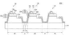
図2は、一実施形態に係る発光素子100Aの断面図を示す。
FIG. 2 shows a cross-sectional view of a
図2に例示した発光素子100Aは、基板110、複数の発光セルD1,D2,D3、電流遮断層140A及び導電型相互連結層150を含む。
The
基板110は、半導体物質の成長に適した物質、キャリアウエハで形成することができる。また、基板110は、熱伝導性に優れた物質で形成することができ、伝導性基板または絶縁性基板であってもよい。また、基板110は、透光性を有する物質からなってもよく、発光セルD1〜D3の全体窒化物発光構造物120a,120bの反りを引き起こさないとともに、スクライビング(scribing)工程及びブレーキング(breading)工程を通じて別個のチップによく分離させるための程度の機械的強度を有することができる。例えば、基板110は、サファイア(Al2O3)、GaN、SiC、ZnO、Si、GaP、InP、Ga2O3、GaAs、Geのうち少なくとも一つを含む物質であってもよい。このような基板110の上面には凹凸パターン形状を有することができる。例えば、たとえ図示していないが、基板110は、PSS(Patterned Sapphire Substrate)であってもよい。
The
また、基板110と発光構造物120a,120bとの間にバッファ層(図示せず)が配置されてもよい。バッファ層は、III−V族元素の化合物半導体を用いて形成することができる。バッファ層は、基板110と発光構造物120a,120bとの間の格子定数の差を減少させる役割を果たす。例えば、バッファ層は、AlNを含むか、またはアンドープ(undoped)窒化物を含むことができるが、これに限定されない。バッファ層は、基板110の種類及び発光構造物120a,120bの種類によって省略してもよい。
In addition, a buffer layer (not shown) may be disposed between the
複数の発光セルD1〜D3は、基板110上に水平方向に互いに離隔して配列される。ここで、説明の便宜上、発光セルD1〜D3の個数は3個である場合を示しているが、本実施形態はこれに限定されず、発光セルが2個であるか、または4個以上である場合にも同一に適用することができる。
The plurality of light emitting cells D1 to D3 are arranged on the
第1発光セルD1は基板110の第1領域A1に配置され、第2発光セルD2は基板110の第2領域A2に配置され、第3発光セルD3は基板110の第3領域A3に配置される。隣接する第1及び第2発光セルD1,D2は一定の距離dだけ互いに離隔して配置され、第2及び第3発光セルD2,D3は一定の距離dだけ互いに離隔して配置される。例えば、離隔距離dは、2μm〜7μm、例えば、5μmであってもよい。
The first light emitting cell D1 is disposed in the first region A1 of the
発光セルD1,D2のそれぞれは、基板110上に配置された発光構造物120a,120b、下部電極132a,132b、上部電極134a,134b及び伝導層160a,160bを含む。
Each of the light emitting cells D1 and D2 includes light emitting
発光構造物120a,120bは、基板110の上部に順次配置された下部半導体層122a,122b、活性層124a,124b及び上部半導体層126a,126bを含む。下部半導体層122a,122bと上部半導体層126a,126bとは互いに異なる導電型であってもよい。
The
下部半導体層122a,122bは、基板110と活性層124a,124bとの間に配置され、半導体化合物を含むことができ、III−V族、II−VI族などの化合物半導体で具現することができ、第1導電型ドーパントがドープされてもよい。例えば、下部半導体層122a,122bは、AlxInyGa(1−x−y)N(0≦x≦1、0≦y≦1、0≦x+y≦1)の組成式を有する半導体物質、InAlGaN、AlGaAs、GaP、GaAs、GaAsP、AlGaInPのいずれか一つ以上を含むことができる。下部半導体層122a,122bは、第1導電型の半導体層であってもよい。もし、下部半導体層122a,122bがn型半導体層である場合、第1導電型ドーパントは、Si、Ge、Sn、Se、Teなどのようなn型ドーパントを含むことができる。下部半導体層122a,122bは、単層または多層構造を有することができ、これに限定しない。
The
活性層124a,124bは、下部半導体層122a,122bと上部半導体層126a,126bとの間に配置され、単一井戸構造、ダブルへテロ構造(Double Hetero Structure)、多重井戸構造、単一量子井戸構造、多重量子井戸(MQW:Multi Quantum Well)構造、量子点構造または量子線構造のいずれか一つを含むことができる。活性層124a,124bは、III−V族元素の化合物半導体材料を用いて、井戸層と障壁層、例えば、InGaN/GaN、InGaN/InGaN、GaN/AlGaN、InAlGaN/GaN、GaAs(InGaAs)/AlGaAs、GaP(InGaP)/AlGaPのいずれか一つ以上のペア構造を有することができるが、これに限定されない。井戸層は、障壁層のエネルギーバンドギャップよりも小さいエネルギーバンドギャップを有する物質からなることができる。
The
上部半導体層126a,126bは、活性層124a,124bの上部に配置され、半導体化合物を含むことができる。上部半導体層126a,126bは、III−V族、II−VI族などの化合物半導体で具現することができ、例えば、InxAlyGa1−x−yN(0≦x≦1、0≦y≦1、0≦x+y≦1)の組成式を有する半導体物質またはAlInN、AlGaAs、GaP、GaAs、GaAsP、AlGaInPのいずれか一つ以上を含むことができる。
The
第1導電型半導体層である下部半導体層122a,122bとは異なり、上部半導体層126a,126bは、第2導電型半導体層であってもよく、第2導電型ドーパントがドープされてもよい。上部半導体層126a,126bがp型半導体層である場合、第2導電型ドーパントは、Mg、Zn、Ca、Sr、Baなどのようなp型ドーパントであってもよい。上部半導体層126a,126bは、単層または多層構造を有することができ、これに限定しない。
Unlike the
下部半導体層122a,122bはn型半導体層であり、上部半導体層126a,126bはp型半導体層で具現したり、または下部半導体層122a,122bはp型半導体層であり、上部半導体層126a,126bはn型半導体層で具現してもよい。これによって、発光構造物120a,120bは、n−p接合、p−n接合、n−p−n接合、及びp−n−p接合構造のうち少なくとも一つを含むことができる。
The
下部電極132a,132bは下部半導体層122a,122b上に配置され、上部電極134a,134bは上部半導体層126a,126b上に配置される。下部電極132a,132bを下部半導体層122a,122b上に配置するために、発光構造物120a,120bは、下部半導体層122a,122bの一部を露出することができる。すなわち、上部半導体層126a,126b、活性層124a,124b及び下部半導体層122a,122bの一部がメサエッチング(mesa etching)によってエッチングされて、下部半導体層122a,122bの一部を露出することができる。このとき、下部半導体層122a,122bの露出面は、活性層124a,124bの下面よりも低く位置することができる。上部電極134a,134b及び下部電極132a,132bについては、図4を参照してより詳細に後述する。
The
一方、電流遮断層140Aの一部は、複数の発光セルのそれぞれ(例えば、D2)の上部電極134bと上部半導体層126bとの間に配置される。このように配置された電流遮断層140Aは、上部電極134bから活性層124bに向かうキャリアがより良く拡散するようにして、活性層124bの光度の向上に寄与できるようにする。
On the other hand, a part of the
第2発光セルD2の上部電極134bは、第2発光セルD2の上部半導体層126bと対向する下部面を有し、第2発光セルD2の上部電極134bと上部半導体層126bとの間に配置される電流遮断層140Aは、上部電極134bと対向する上部面を有すると仮定する。このとき、電流遮断層140Aが、前述したように、キャリアを拡散させる役割を果たすためには、上部半導体層126b上に配置される電流遮断層140Aの上部面の面積は、上部電極134bの下部面全体の面積以上とすることができる。すなわち、図2に例示した断面形状において、幅W1は、0以上とすることができる。そのために、電流遮断層140Aは、シリコンオキサイド(SiO2)のような絶縁物質で形成することができる。
The
発光セル(例えば、D1,D2)のそれぞれにおいて、伝導層160a,160bは、上部電極134a,134bと電流遮断層140Aとの間から上部半導体層126a,126bの上に延びて配置されることで、上部電極134a,134bと上部半導体層126a,126bとを電気的に接続する。
In each of the light emitting cells (for example, D1 and D2), the
伝導層160a,160bは、全反射を減少させるだけでなく、透光性が良いので、活性層124a,124bから放出されて上部半導体層126a,126bを経た光の抽出効率を増加させることができる。伝導層160a,160bは、発光波長に対して透過率の高い透明な酸化物系物質、例えば、ITO(Indium Tin Oxide)、TO(Tin Oxide)、IZO(Indium Zinc Oxide)、IZTO(Indium Zinc Tin Oxide)、IAZO(Indium Aluminium Zinc Oxide)、IGZO(Indium Gallium Zinc Oxide)、IGTO(Indium Gallium Tin Oxide)、AZO(Aluminium Zinc Oxide)、ATO(Aluminium Tin Oxide)、GZO(Gallium Zinc Oxide)、IrOx、RuOx、RuOx/ITO、Ni、Ag、Ni/IrOx/AuまたはNi/IrOx/Au/ITOのうち少なくとも一つ以上を用いて単層または多層で具現することができる。
The
上部半導体層126a,126bの上部に配置された伝導層160a,160bの面積は、上部半導体層126a,126bの上部面の面積以下とすることができる。したがって、図2に例示したように、幅W2は、0以上とすることができる。
The areas of the
一方、導電型相互連結層150は、複数の発光セルD1〜D3において隣接する二つの発光セル(例えば、D1,D2)を接続する役割を果たす。すなわち、導電型相互連結層150は、隣接する二つの発光セルD1,D2のうち一方である第1発光セルD1の下部電極132aと、隣接する発光セルD1,D2のうち他方である第2発光セルD2の上部電極134bとを電気的に接続する役割を果たす。図2に例示したように、二つの発光セルD1,D2は、導電型相互連結層150によって電気的に互いに直列接続されてもよいが、これに限定されない。すなわち、発光セルD1,D2は、導電型相互連結層150によって電気的に互いに並列に接続されてもよい。
Meanwhile, the
導電型相互連結層150は、下部電極132a,132b及び/又は上部電極134a,134bと同一または互いに異なる構成、及び同一または互いに異なる物質からなることができる。また、導電型相互連結層150の厚さは、下部電極132a,132b及び/又は上部電極134a,134bの厚さと同一または互いに異なっていてもよい。導電型相互連結層150は、Cr、Rd、Au、Ni、TiまたはPtのうち少なくとも一つを含むことができるが、これに限定されない。
The
一方、本実施形態によれば、電流遮断層140Aは、発光セル(例えば、D2)の上部電極134bと上部半導体層126bとの間から隣接する発光セルD1,D2と導電型相互連結層150との間に延びて配置され得る。すなわち、電流遮断層140Aは、第1発光セルD1の下部半導体層122aと導電型相互連結層150との間、基板110と導電型相互連結層150との間、及び第2発光セルD2の発光構造物120bと導電型相互連結層150との間に配置することができる。したがって、図2に例示した電流遮断層140Aは、図1に示されたパッシベーション層60の役割をすることがわかる。そのために、前述したように、電流遮断層140Aは、絶縁物質からなることができる。
On the other hand, according to the present embodiment, the
前述したように、図1に示された発光素子が別途のパッシベーション層60を設ける代わりに、本実施形態による発光素子100Aは、電流遮断層140Aがパッシベーション層60の役割を果たす。すなわち、電流遮断層140Aは、電流遮断層固有の役割を果たすことができるだけでなく、パッシベーション層60の役割も果たすことができる。したがって、作製コストを低減し、工程時間を短縮させることができる。
As described above, the
図3は、他の実施形態による発光素子100Bの断面図を示す。 FIG. 3 is a cross-sectional view of a light emitting device 100B according to another embodiment.
図2に例示した発光素子100Aにおいて、電流遮断層140Aは単一層として具現されている。反面、他の実施形態によれば、図3に例示したように、電流遮断層140Bは、分散ブラッグ反射層(DBR:Distributed Bragg Reflector)として具現されてもよい。分散ブラッグ反射層とは、屈折率の互いに異なる二つ以上の絶縁層が交互に複数層に積層されて生成されることによって反射率を高める層を意味する。分散ブラッグ反射層140Bは、90%以下の反射率を有する反射層よりもさらに高い反射率、例えば、98%の反射率を有するので、より効率よく反射層の役割を果たすことができる。
In the
図3の場合、屈折率の互いに異なる第1層142及び第2層144が交互に1回積層された姿を示しているが、1回よりさらに多くの回数積層されてもよい。
In the case of FIG. 3, the
第1層142は、低屈折率層であって、例えば、1.4の屈折率を有するシリコン酸化物(SiO2)または1.6の屈折率を有するアルミニウム酸化物(Al2O3)からなることができる。また、第2層144は、高屈折率層であって、例えば、2.05〜2.25の屈折率を有するシリコン窒化物(Si3N4)、2以上の屈折率を有するチタン窒化物(TiO2)、または3以上の屈折率を有するSi−Hからなることができる。
The
また、分散ブラッグ反射層140Bにおいて、第1層142及び第2層144のそれぞれは、λ/(4n)の厚さを有することができる。ここで、λは、活性層124bから放出された光の波長を示し、nは、該当の層の屈折率を示す。
In the distributed
また、図2に例示した発光素子100Aにおいて、隣接する発光セル(例えば、D1及びD2)のいずれか一方である第1発光セルD1の下部電極132aと、隣接する発光セルのうち他方である第2発光セルD2の上部電極134b、及びこれら(D1,D2)を電気的に接続させる導電型相互連結層150は、それぞれ別個に形成されている。反面、他の実施形態によれば、図3に例示したように、導電型相互連結層150、第1発光セルD1の下部電極132a及び第2発光セルD2の上部電極134bは、互いに一体型層170Aとして具現されてもよい。
Further, in the
もし、一体型層170が、第2発光セルD2の上部で上部半導体層126bと対向する下部面を有し、一体型層170Aと上部半導体層126bとの間に配置される電流遮断層140Bが、一体型層170Aと対向する上部面を有するとする時、電流遮断層140Bの上部面の面積は、一体型層170Aの下部面全体の面積以上とすることができる。これは、図3に例示したように、第2発光セルD2の上部電極134bと導電型相互連結層150とが一体型層170Aとして具現される場合、一体型層170Aと上部半導体層126bとの間に介在して配置された電流遮断層140Bが、前述したように、一体型層170Aから活性層124bに供給されるキャリアをより良く拡散させて、電流を遮断させる役割を果たすようにするためである。
If the integrated layer 170 has a lower surface facing the
前述した図2と図3の差異点を除いては、図3に例示した発光素子100Bは、図2に例示した発光素子100Aと同一であるので、これについての詳細な説明を省略する。
Except for the difference between FIG. 2 and FIG. 3 described above, the light emitting element 100B illustrated in FIG. 3 is the same as the
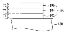
図4は、図2又は図3に例示した下部電極132a,132b、上部電極134a,134b、導電型相互連結層150及び一体型層170Aのうち少なくとも一つの実施形態の断面図を示す。
FIG. 4 is a cross-sectional view of at least one embodiment of the
もし、図4の層190が下部電極132a,132bに該当すると、ベース層180は下部半導体層122a,122bに該当し、層190が上部電極134a,134bに該当すると、ベース層180は伝導層160a,160bに該当し、層190が導電型相互連結層150または一体型層170Aに該当すると、ベース層180は電流遮断層140A,140Bに該当する。
4 corresponds to the
図4を参照すると、層190は、互いに重なる接着層192及びボンディング層196を含むことができる。すなわち、接着層192はベース層180の上に配置し、ボンディング層196は接着層192の上に配置することができる。このとき、接着層192とボンディング層196との間に反射層(図示せず)が介在してもよく、介在しなくてもよい。
Referring to FIG. 4, the layer 190 may include an
接着層192は、ベース層180とオーミック接触する物質を含むことができる。例えば、接着層192は、Cr、Rd及びTiのうち少なくとも一つの材料で、単層または多層構造で形成することができる。また、接着層192の厚さT1は、少なくとも5nm〜15nmであってもよい。例えば、接着層192は、2nm〜10nmの厚さT1を有することができる。
The
また、ボンディング層196は、接着層192に接して配置されてもよいが、図4に例示したように、バリア層194が介在する場合、バリア層194の上部に配置されてもよい。ボンディング層196は、Auを含むことができ、100nm〜180nmの厚さT2、例えば、140nmの厚さを有することができる。
The
層190は、接着層192とボンディング層196との間に配置されたバリア層194をさらに含むことができるが、バリア層194は省略してもよい。バリア層194は、接着層192及びボンディング層196にそれぞれ接して配置することができる。
The layer 190 may further include a barrier layer 194 disposed between the
バリア層194は、Ni、Cr、Ti及びPtのうち少なくとも一つを含む材料で、単層または多層に形成することができる。例えば、バリア層194は、CrとPtの合金からなることができる。また、バリア層194は、200nm〜300nm、例えば、250nmの厚さT3を有することができる。 The barrier layer 194 is made of a material containing at least one of Ni, Cr, Ti, and Pt, and can be formed in a single layer or multiple layers. For example, the barrier layer 194 can be made of an alloy of Cr and Pt. Further, the barrier layer 194 can have a thickness T3 of 200 nm to 300 nm, for example, 250 nm.
もし、層190が上部電極134a,134bである場合において、接着層192とバリア層194との間に反射層が介在する場合、反射層は、活性層124a,124bから放出された光を反射させることで、層190の金属によって吸収される光量を減少させることができる。しかし、反射層が接着層192とバリア層194との間に介在する場合、Auからなるボンディング層196及びAlからなる反射層が、Niからなるバリア層194を挟んで互いに相互拡散(inter−diffusion)されることもある。
If the layer 190 is the
また、十分な反射度を得るために、反射層は、通常、50nm〜300nmの厚さに形成することができる。このような厚い反射層の存在のため、接着層192が、例えば、2nmよりも薄い厚さに形成されて、層190と発光構造物120a,120bとの接着力が低下することがある。
In order to obtain sufficient reflectivity, the reflective layer can be usually formed to a thickness of 50 nm to 300 nm. Due to the presence of such a thick reflective layer, the
しかし、接着層192とボンディング層196との間に反射層が介在しない場合、反射層が介在しない厚さの分だけ接着層192を厚く形成することができるので、層190とベース層180との接着力を向上させることができ、反射層とボンディング層196間の相互拡散が発生するおそれもなくすことができる。このとき、接着層192は、2nm以上の厚い厚さT1を有することができる。
However, in the case where no reflective layer is interposed between the
また、前述した発光素子100A,100Bが照明用に使用される場合、反射層であるアルミニウムが腐食し得る。したがって、本実施形態において、反射層を介在しない場合、このような腐食の問題を事前に予防できるので、発光素子100A,100Bを外部照明用に使用することができる。
In addition, when the above-described
図5は、更に他の実施形態による発光素子100Cの断面図を示す。
FIG. 5 is a cross-sectional view of a
図3に示された発光素子100Bにおいて一体型層170Aは単一層である反面、図5に例示した発光素子100Cの一体型層170Bは、接着層172、バリア層174及びボンディング層176を含むことができる。それを除いては、図5に例示した発光素子100Cは、図3に例示した発光素子100Bと同一であるので、これについての詳細な説明を省略する。図5に例示した接着層172、バリア層174及びボンディング層176は、図4に示された接着層192、バリア層194及びボンディング層196にそれぞれ該当するので、これについての詳細な説明を省略する。図5の場合、一体型層170Bにおいてバリア層174は省略してもよい。
In the light emitting device 100B illustrated in FIG. 3, the
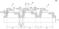
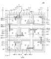
図6は、更に他の実施形態に係る発光素子100Dの平面図を示し、図7は、図6に示された‘K’部分の拡大図であり、図8は、図6に示された発光素子100DのA−A’線に沿って切断した断面図を示し、図9は、図6に示された発光素子100DのB−B’線に沿って切断した断面図を示す。
6 is a plan view of a
図6乃至図9を参照すると、発光素子100Dは、M個の発光領域P1〜PM(M>1である自然数)を含む。説明の便宜上、図6乃至図9に示したように、M=9であると仮定して説明するが、Mが9よりも小さいか、または大きい場合にも、実施形態は同一に適用することができる。
Referring to FIGS. 6 to 9, the
発光素子100Dは、基板110、複数の発光領域P1〜P9として区分される発光構造物120−1〜120−9、電流遮断層140A−1〜140A−9、一体型層170A−1〜170A−8、第1電極152、第2電極154及び伝導層160−1〜160−9を含む。
The
基板110及び発光構造物120−1〜120−9は、図2又は図3の基板110及び発光構造物120a,120bにそれぞれ該当するので、これらについての詳細な説明を省略する。各発光構造物120−1〜120−9は、図2及び図3に示された下部半導体層122a,122b、活性層124a,124b及び上部半導体層126a,126bにそれぞれ該当する下部半導体層122−1〜122−9、活性層124−1〜124−9及び上部半導体層126−1〜126−9を含む。
Since the
以下、下部半導体層122−1〜122−9のそれぞれはn型半導体層で、上部半導体層126−1〜126−9のそれぞれはp型半導体層であると仮定して実施形態を説明するが、実施形態はこれに限定されない。すなわち、下部半導体層122−1〜122−9のそれぞれはp型半導体層で、上部半導体層126−1〜126−9のそれぞれはn型半導体層である場合にも本実施形態は適用可能である。 Hereinafter, the embodiment will be described on the assumption that each of the lower semiconductor layers 122-1 to 122-9 is an n-type semiconductor layer and each of the upper semiconductor layers 126-1 to 126-9 is a p-type semiconductor layer. The embodiment is not limited to this. In other words, the present embodiment can also be applied to the case where each of the lower semiconductor layers 122-1 to 122-9 is a p-type semiconductor layer and each of the upper semiconductor layers 126-1 to 126-9 is an n-type semiconductor layer. is there.
一つのチップ(single chip)の発光構造物120−1〜120−9は、境界領域Sによって複数個の発光領域P1〜P9に区分することができる。境界領域Sは、発光領域P1〜P9のそれぞれの周りに位置する領域であってもよく、基板110であってもよい。複数の発光領域P1〜P9のそれぞれの面積は同一であってもよいが、これに限定されるものではない。
The light emitting structures 120-1 to 120-9 of one chip can be divided into a plurality of light emitting regions P1 to P9 according to the boundary region S. The boundary region S may be a region located around each of the light emitting regions P1 to P9, or may be the
電流遮断層140A−1〜140A−9のそれぞれは、図2に示された電流遮断層140Aと同一であるので、これについての詳細な説明は省略する。ただし、電流遮断層140A−1〜140A−9のうち電流遮断層140A−1は、パッシベーション層60の役割を果たさずに、第1電極152から活性層124−1に向かうキャリアが拡散するようにして、活性層124−1の光度の向上に寄与できるようにする役割のみを果たす。
Since each of the current blocking layers 140A-1 to 140A-9 is the same as the
図6及び図8を参照すると、第1電極152は、複数の発光領域P1〜P9のいずれか一つの発光領域(例えば、P1)の上部半導体層126−1上に配置される。第1電極152は、伝導層160−1を経由して上部半導体層126−1と電気的に接触することができる。例えば、第1電極152は、直列接続される発光領域P1〜P9のうち1番目の発光領域(例えば、P1)の伝導層160−1と接触することができる。第1電極152は、第1電源を提供するためのワイヤ(図示せず)がボンディングされ得る。
Referring to FIGS. 6 and 8, the
図6及び図9を参照すると、第2電極154は、複数の発光領域P1〜P9のいずれか一つの発光領域(例えば、P9)の下部半導体層122−9上に配置され、下部半導体層122−9と接触することができる。第2電極154は、第2電源を提供するためのワイヤ(図示せず)がボンディングされ得る。
Referring to FIGS. 6 and 9, the
一体型層170A−1〜170A−8は、電流遮断層140A−2〜140A−9上にそれぞれ配置され、複数の発光領域P1〜P9を電気的に直列接続する。例えば、一体型層170A−1〜170A−8は、第1電極152が位置する第1発光領域P1を始点とし、第2電極154が位置する第9発光領域P9を終点として複数の発光領域P1〜P9を直列接続することができる。
The integrated layers 170A-1 to 170A-8 are disposed on the current blocking layers 140A-2 to 140A-9, respectively, and electrically connect the plurality of light emitting regions P1 to P9 in series. For example, the
一体型層170A−1〜170A−8のそれぞれは、図3に示された一体型層170Aと同一であるので、これについての詳細な説明は省略する。各一体型層(例えば、170A−1)は、隣接する発光領域(例えば、P1及びP2)のいずれか一方の発光領域P1の下部半導体層122−1と残りの他方の発光領域(例えば、P2)の伝導層160−2とを互いに電気的に接続することができる。
Since each of the
図6乃至図8を参照すると、一体型層(例えば、170A−2)と上部半導体層(例えば、126−3)の上部面との間に配置された電流遮断層(例えば、140A−3)は、一体型層170A−2と対向する上部面を有するとする。また、一体型層170A−2は、上部半導体層126−3と対向する下部面を有するとする。このとき、電流遮断層140A−3の上部面の面積は、一体型層170A−2の下部面全体の面積以上とすることができる。これは、一体型層170A−2と上部半導体層126−3との間に介在して配置された電流遮断層140A−3が、一体型層170A−2から活性層124−3に供給されるキャリアを拡散させて電流を遮断させるようにするためである。このとき、電流遮断層140A−3の上部面は、一体型層170A−2の下部面よりさらに大きくすることができる。この場合、図7に例示したように、電流遮断層140A−3の幅は、一体型層170A−2の幅よりも第1方向にd1+d2だけさらに広くし、図8に例示したように、第2方向にW1だけさらに広くすることができる。
Referring to FIGS. 6 to 8, a current blocking layer (eg, 140A-3) disposed between the monolithic layer (eg, 170A-2) and the upper surface of the upper semiconductor layer (eg, 126-3). Has an upper surface facing the
発光素子100Dに含まれる互いに直列接続される複数の発光領域P1〜P9を順に第1発光領域〜第9発光領域という。すなわち、第1電極152が位置する発光領域を第1発光領域P1といい、第2電極154が位置する発光領域を第9発光領域という。ここで、“隣接する発光領域”は、第k発光領域と第k+1発光領域とすることができ、第k一体型層は、第k発光領域と第k+1発光領域とを電気的に直列接続することができ、1≦k≦(M−1)とすることができる。
The plurality of light emitting regions P1 to P9 connected in series included in the
すなわち、第k一体型層は、第k発光領域の下部半導体層122−kと第k+1発光領域の伝導層160−(k+1)とを電気的に接続することができる。例えば、図8を参照すると、第2一体型層170A−2は、第2発光領域P2、第3発光領域P3及びそれらの間の境界領域S上に位置することができる。そして、第2一体型層170A−2は、第2発光領域P2の下部半導体層122−2及び第3発光領域P3の伝導層160−3を経由して、上部半導体層126−3を電気的に接続する。
That is, the k-th integrated layer can electrically connect the lower semiconductor layer 122-k in the k-th light emitting region and the conductive layer 160- (k + 1) in the k + 1 light-emitting region. For example, referring to FIG. 8, the second
このとき、第k+1電流遮断層140A−(k+1)は、第k一体型層170A−kと第k下部半導体層122−kとの間、第k一体型層170A−kと基板110との間、第k一体型層170A−kと第k+1下部半導体層122−(k+1)との間、第k一体型層170A−kと第k+1活性層124−(k+1)との間、第k一体型層170−kと第k+1上部半導体層126−(k+1)との間に位置して互いを電気的に絶縁させることができる。
At this time, the (k + 1) th
図8又は図9に例示したものとは異なり、電流遮断層140A−1〜140−9は、図3に例示したように、分散ブラッグ反射層140Bとして具現することができる。この場合、第1電極152及び一体型層170A−1〜170A−8に光が吸収されて損失が生じることを遮断することによって、発光効率を向上させることができる。
Unlike those illustrated in FIG. 8 or FIG. 9, the current blocking layers 140 </ b> A- 1 to 140-9 can be implemented as a distributed Bragg reflection layer 140 </ b> B as illustrated in FIG. 3. In this case, the light emission efficiency can be improved by blocking the loss of light that is absorbed by the
図10は、図6に示された発光素子100Dの回路図を示す。
FIG. 10 is a circuit diagram of the
図6及び図10を参照すると、発光素子100Dは、共通した一つの(+)端子152と共通した一つの(−)端子154とを有することができる。
Referring to FIGS. 6 and 10, the light emitting device 100 </ b> D may have a common (+) terminal 152 and a common (−)
図11は、更に他の実施形態に係る発光素子100Eの断面図を示す。
FIG. 11 shows a cross-sectional view of a
図11を参照すると、発光素子100Eは、サブマウント(submount)204、第1金属層232、第2金属層234、第1バンプ部210、第2バンプ部220及び発光素子240を含む。
Referring to FIG. 11, the light emitting device 100 </ b> E includes a
図11の発光素子100Eは、フリップチップ形態で具現した一例であるが、実施形態はこれに限定されるものではなく、他の実施形態に係る発光素子100A〜100Cが、図11に示されたようなフリップチップ形態で具現されてもよい。
The
サブマウント204は、発光素子240を実装する。サブマウント204は、パッケージボディー(package body)または印刷回路基板(Printed Circuit Board)などとして具現することができ、発光素子240がフリップチップボンディング(flip chip bonding)可能な様々な形態を有することができる。
The
発光素子240は、サブマウント204上に配置され、第1バンプ部210及び第2バンプ部220によってサブマウント204と電気的に接続される。図11に示した発光素子240は、図6に示した発光素子100Dの第1及び第9発光領域P1,P9と同一の断面を有する。したがって、同一の部分については詳細な説明を省略する。
The
サブマウント204は、ポリフタルアミド(PolyPhthal Amide、PPA)、液晶高分子(Liquid Crystal Polymer、LCP)、ポリアミド9T(PolyAmide9T、PA9T)などのような樹脂、金属、感光性ガラス(photo sensitive glass)、サファイア、セラミック、印刷回路基板(Printed Circuit Board)などを含むことができる。しかし、実施形態に係るサブマウント204が、これらの物質に限定されるものではない。
The
第1金属層232及び第2金属層234は、サブマウント204の上面に水平方向に互いに離隔して配置される。ここで、サブマウント204の上面は、発光素子240に対向する面であり得る。第1金属層232及び第2金属層234は、伝導性金属、例えば、アルミニウム(Al)またはロジウム(Rh)であってもよい。
The
第1バンプ部210及び第2バンプ部220は、サブマウント204と発光素子240との間に配置される。第1バンプ部210は、第2電極154と第1金属層232とを電気的に接続することができる。第2バンプ部220は、第1電極152と第2金属層234とを電気的に接続することができる。
The first bump part 210 and the
第1バンプ部210は、第1拡散防止接着層212、第1バンパー(bumper)214及び第2拡散防止接着層216を含む。第1バンパー214は、第2電極154と第1金属層232との間に位置する。第1拡散防止接着層212は、第2電極154と第1バンパー214との間に位置し、第1バンパー214と第2電極154を互いに接合させる。すなわち、第1拡散防止接着層212は、第1バンパー214と第2電極154との接着力を向上させ、第1バンパー214に含まれたイオンが第2電極154を通じて発光構造物120−9に浸透または拡散することを防止する役割を果たす。
The first bump part 210 includes a first diffusion preventing
第2拡散防止接着層216は、第1バンパー214と第1金属層232との間に配置され、第1バンパー214と第1金属層232を接合させる。第2拡散防止接着層216は、第1バンパー214と第1金属層232との接着力を向上させ、第1バンパー214に含まれたイオンが第1金属層232を通じてサブマウント204に浸透または拡散することを防止する役割を果たす。
The second diffusion preventing
第2バンプ部220は、第3拡散防止接着層222、第2バンパー224、及び第4拡散防止接着層226を含む。第2バンパー224は、第1電極152と第2金属層234との間に位置する。
The
第3拡散防止接着層222は、第1電極152と第2バンパー224との間に位置し、両者を互いに接合させる。すなわち、第3拡散防止接着層222は、接着力を向上させ、第2バンパー224に含まれたイオンが第1電極152を通じて発光構造物120−1に浸透または拡散することを防止する役割を果たす。
The third anti-diffusion adhesive layer 222 is located between the
第4拡散防止接着層226は、第2バンパー224と第2金属層234との間に配置され、第2バンパー224と第2金属層234を接合させる。第4拡散防止接着層226は、第2バンパー224と第2金属層234との接着力を向上させ、第2バンパー224に含まれたイオンが第2金属層234を通じてサブマウント204に浸透または拡散することを防止する役割を果たす。
The fourth anti-diffusion adhesive layer 226 is disposed between the
第1乃至第4拡散防止接着層212,216,222,226は、Pt、Ti、W/Ti、Auのうち少なくとも一つまたはこれらの合金であってもよい。また、第1バンプ214及び第2バンプ224は、チタン(Ti)、銅(Cu)、ニッケル(Ni)、金(Au)、クロム(Cr)、タンタル(Ta)、白金(Pt)、及び錫(Sn)のうち少なくとも一つを含むことができる。
The first to fourth diffusion preventing
前述した実施形態に係る発光素子の複数個を基板上に発光素子パッケージとして配列することができ、発光素子パッケージの光経路上に光学部材である導光板、プリズムシート、拡散シートなどを配置することができる。このような発光素子パッケージ、基板、光学部材は、バックライトユニットとして機能することができる。 A plurality of light emitting devices according to the above-described embodiments can be arranged as a light emitting device package on a substrate, and a light guide plate, a prism sheet, a diffusion sheet, or the like, which is an optical member, is disposed on the light path of the light emitting device package. Can do. Such a light emitting device package, a substrate, and an optical member can function as a backlight unit.
更に他の実施形態は、上述した実施形態に記載された発光素子または発光素子パッケージを含む表示装置、指示装置、照明システムとして具現することができ、例えば、照明システムは、ランプ、街灯を含むことができる。 Still other embodiments can be embodied as a display device, a pointing device, or a lighting system including the light emitting device or the light emitting device package described in the above embodiments. For example, the lighting system includes a lamp and a streetlight. Can do.
図12は、上述した実施形態に係る発光素子によって具現される発光素子パッケージを含む照明装置の分解斜視図である。図12を参照すると、照明装置は、光を投射する光源750と、光源750が内蔵されるハウジング700と、光源750の熱を放出する放熱部740と、光源750及び放熱部740をハウジング700に結合するホルダー760と、を含む。
FIG. 12 is an exploded perspective view of a lighting apparatus including a light emitting device package embodied by the light emitting device according to the above-described embodiment. Referring to FIG. 12, the lighting device includes a
ハウジング700は、電気ソケット(図示せず)に結合されるソケット結合部710と、ソケット結合部710と連結され、光源750が内蔵されるボディー部730とを含む。ボディー部730には、一つの空気流動口720が貫通して形成されてもよい。
The
ハウジング700のボディー部730上に複数個の空気流動口720が備えられ、空気流動口720は一つまたは複数個であってもよい。空気流動口720は、ボディー部730に放射状に配置したり、様々な形態で配置することができる。
A plurality of
光源750は、基板754上に備えられる複数個の発光素子パッケージ752を含む。基板754は、ハウジング700の開口部に挿入可能な形状とすることができ、後述するように、放熱部740に熱を伝達するために熱伝導率の高い物質からなることができる。複数個の発光素子パッケージは、前述した発光素子を含むことができる。
The
光源750の下部にはホルダー760が備えられ、ホルダー760は、フレーム及び他の空気流動口を含むことができる。また、図示していないが、光源750の下部には光学部材が備えられて、光源750の発光素子パッケージ752から投射される光を拡散、散乱または収斂させることができる。
A lower portion of the
図13は、上述した実施形態に係る発光素子によって具現される発光素子パッケージを含む表示装置を示す。 FIG. 13 illustrates a display device including a light emitting device package embodied by the light emitting device according to the above-described embodiment.
図13を参照すると、表示装置800は、ボトムカバー810と、ボトムカバー810上に配置される反射板820と、光を放出する発光モジュール830,835と、反射板820の前方に配置され、前記発光モジュール830,835から発散される光を表示装置の前方に案内する導光板840と、導光板840の前方に配置されるプリズムシート850,860を含む光学シートと、光学シートの前方に配置されるディスプレイパネル870と、ディスプレイパネル870と連結され、ディスプレイパネル870に画像信号を供給する画像信号出力回路872と、ディスプレイパネル870の前方に配置されるカラーフィルター880とを含むことができる。ここで、ボトムカバー810、反射板820、発光モジュール830,835、導光板840、及び光学シートはバックライトユニット(Backlight Unit)をなすことができる。
Referring to FIG. 13, a
発光モジュールは、基板830上の発光素子パッケージ835を含んでなる。ここで、基板830としてはPCBなどを使用することができる。発光素子パッケージ835は、前述した実施形態に係る発光素子を含むことができる。
The light emitting module includes a light emitting
ボトムカバー810は、表示装置800内の構成要素を収納することができる。そして、反射板820は、同図のように別途の構成要素として設けてもよく、導光板840の後面やボトムカバー810の前面に反射度の高い物質でコーティングする形態で設けることも可能である。
The
ここで、反射板820は、反射率が高く、超薄型に形成可能な素材を使用することができ、ポリエチレンテレフタレート(PolyEthylene Terephtalate;PET)を使用することができる。
Here, the
そして、導光板840は、ポリメチルメタクリレート(PolyMethylMethACrylate;PMMA)、ポリカーボネート(PolyCarbonate;PC)、またはポリエチレン(PolyEthylene;PE)などで形成することができる。
The
そして、第1プリズムシート850は、支持フィルムの一面に、透光性で且つ弾性を有する重合体材料で形成することができ、重合体は、複数個の立体構造が反復して形成されたプリズム層を有することができる。ここで、複数個のパターンは、図示のように、山と谷が反復的にストライプ状に備えられてもよい。
The
そして、第2プリズムシート860において支持フィルムの一面の山と谷の方向は、第1プリズムシート850内の支持フィルムの一面の山と谷の方向と垂直をなすことができる。これは、発光モジュールと反射シートから伝達された光をディスプレイパネル870の全面に均一に分散させるためである。
In the
そして、図示していないが、導光板840と第1プリズムシート850との間に拡散シートが配置されてもよい。拡散シートは、ポリエステルとポリカーボネート系列の材料からなることができ、バックライトユニットから入射された光を、屈折及び散乱を通じて光投射角を最大に広げることができる。そして、拡散シートは、光拡散剤を含む支持層と、光出射面(第1プリズムシート方向)と光入射面(反射シート方向)に形成され、光拡散剤を含んでいない第1レイヤー及び第2レイヤーを含むことができる。
Although not shown, a diffusion sheet may be disposed between the
実施形態において、拡散シート、第1プリズムシート850、及び第2プリズムシート860が光学シートを構成するが、光学シートは、他の組み合わせ、例えば、マイクロレンズアレイからなってもよく、拡散シートとマイクロレンズアレイとの組み合わせ、または一つのプリズムシートとマイクロレンズアレイとの組み合わせなどからなってもよい。
In the embodiment, the diffusion sheet, the
ディスプレイパネル870としては液晶表示パネル(Liquid crystal display)を配置してもよいが、液晶表示パネル以外に、光源を必要とする他の種類の表示装置を備えてもよい。
As the
以上、実施形態を中心に説明したが、これは単なる例示であり、本発明を限定するものではなく、本発明の属する分野における通常の知識を有する者であれば、本実施形態の本質的な特性を逸脱しない範囲で、以上で例示していない様々な変形及び応用が可能であるということが理解されるであろう。例えば、実施形態に具体的に示した各構成要素は変形実施が可能である。そして、このような変形及び応用に係る差異点は、添付の特許請求の範囲で規定する本発明の範囲に含まれるものと解釈しなければならない。 Although the embodiment has been mainly described above, this is merely an example and is not intended to limit the present invention. Any person having ordinary knowledge in the field to which the present invention belongs can be used. It will be understood that various modifications and applications not exemplified above are possible without departing from the characteristics. For example, each component specifically shown in the embodiment can be modified. Such differences in modification and application should be construed as being included in the scope of the present invention as defined in the appended claims.
Claims (10)
前記基板上に水平方向に互いに離隔して配列され、それぞれは、互いに異なる導電型の下部及び上部半導体層、前記下部及び上部半導体層の間に配置された活性層を有する発光構造物と、前記上部半導体層上に配置された上部電極と、前記下部半導体層上に配置された下部電極とを含む複数の発光セルと、
隣接する複数の発光セルのうち一方の第1発光セルの下部電極と、前記隣接する複数の発光セルのうち他方の第2発光セルの上部電極とを電気的に接続する導電型相互連結層と、
前記第2発光セルの上部電極と上部半導体層との間から前記隣接する複数の発光セルと前記導電型相互連結層との間に延びて配置された電流遮断層とを含み、
前記複数の発光セルのそれぞれは、
前記第2発光セルの上部電極と前記電流遮断層との間から前記第2発光セルの上部半導体層の上に延びて配置されて、前記第2発光セルの上部電極と第2発光セルの上部半導体層とを電気的に接続する伝導層をさらに含む、発光素子。 A substrate,
A light emitting structure that is horizontally spaced apart from each other on the substrate, each having a lower and upper semiconductor layer of different conductivity types, and an active layer disposed between the lower and upper semiconductor layers; A plurality of light emitting cells including an upper electrode disposed on the upper semiconductor layer and a lower electrode disposed on the lower semiconductor layer;
A conductive interconnection layer that electrically connects a lower electrode of one first light emitting cell among the plurality of adjacent light emitting cells and an upper electrode of the other second light emitting cell among the plurality of adjacent light emitting cells; ,
A current blocking layer disposed between the plurality of adjacent light emitting cells and the conductive interconnection layer from between the upper electrode and the upper semiconductor layer of the second light emitting cell;
Each of the plurality of light emitting cells is
An upper electrode of the second light emitting cell and an upper portion of the second light emitting cell are disposed extending between the upper electrode of the second light emitting cell and the current blocking layer on the upper semiconductor layer of the second light emitting cell. A light emitting device further comprising a conductive layer electrically connecting the semiconductor layer.
前記第1発光セルの下部半導体層と前記導電型相互連結層との間、前記基板と前記導電型相互連結層との間、及び前記第2発光セルの発光構造物と前記導電型相互連結層との間に配置される、請求項1に記載の発光素子。 The current blocking layer is
Between the lower semiconductor layer of the first light emitting cell and the conductive interconnect layer, between the substrate and the conductive interconnect layer, and the light emitting structure of the second light emitting cell and the conductive interconnect layer. The light emitting device according to claim 1, which is disposed between the two.
前記第2発光セルの上部電極と上部半導体層との間に配置される前記電流遮断層は、前記上部電極と対向する上部面を有し、
前記電流遮断層の上部面の面積は、前記上部電極の下部面全体の面積以上である、請求項1又は2に記載の発光素子。 The upper electrode of the second light emitting cell has a lower surface facing the upper semiconductor layer of the second light emitting cell,
The current blocking layer disposed between the upper electrode of the second light emitting cell and the upper semiconductor layer has an upper surface facing the upper electrode;
3. The light emitting device according to claim 1, wherein an area of an upper surface of the current blocking layer is equal to or greater than an area of an entire lower surface of the upper electrode.
前記一体型層と前記第2発光セルの上部半導体層との間に配置される前記電流遮断層は、前記一体型層と対向する上部面を有し、
前記電流遮断層の上部面の面積は、前記一体型層の下部面全体の面積以上である、請求項4に記載の発光素子。 The integrated layer has a lower surface facing the upper semiconductor layer of the second light emitting cell;
The current blocking layer disposed between the integrated layer and the upper semiconductor layer of the second light emitting cell has an upper surface facing the integrated layer;
The light emitting device according to claim 4, wherein an area of the upper surface of the current blocking layer is equal to or larger than an area of the entire lower surface of the integrated layer.
互いに重なる第1接着層及び第1ボンディング層を含み、前記第1接着層と前記第1ボンディング層との間に反射層が介在していない、請求項1ないし8のいずれかに記載の発光素子。 The upper electrode is
9. The light emitting device according to claim 1, comprising a first adhesive layer and a first bonding layer that overlap each other, wherein no reflective layer is interposed between the first adhesive layer and the first bonding layer. .
互いに重なる第2接着層及び第2ボンディング層を含み、前記第2接着層と前記第2ボンディング層との間に反射層が介在していない、請求項1ないし9のいずれかに記載の発光素子。 The lower electrode is
10. The light emitting device according to claim 1, comprising a second adhesive layer and a second bonding layer overlapping each other, wherein no reflective layer is interposed between the second adhesive layer and the second bonding layer. .
Applications Claiming Priority (2)
| Application Number | Priority Date | Filing Date | Title |
|---|---|---|---|
| KR1020120141503A KR20140073351A (en) | 2012-12-06 | 2012-12-06 | Light Emitting Device |
| KR10-2012-0141503 | 2012-12-06 |
Publications (2)
| Publication Number | Publication Date |
|---|---|
| JP2014116604A true JP2014116604A (en) | 2014-06-26 |
| JP2014116604A5 JP2014116604A5 (en) | 2017-01-12 |
Family
ID=49683623
Family Applications (1)
| Application Number | Title | Priority Date | Filing Date |
|---|---|---|---|
| JP2013251766A Pending JP2014116604A (en) | 2012-12-06 | 2013-12-05 | Light emitting device |
Country Status (5)
| Country | Link |
|---|---|
| US (2) | US9337236B2 (en) |
| EP (1) | EP2741338B1 (en) |
| JP (1) | JP2014116604A (en) |
| KR (1) | KR20140073351A (en) |
| CN (1) | CN103855180B (en) |
Cited By (7)
| Publication number | Priority date | Publication date | Assignee | Title |
|---|---|---|---|---|
| JP2016012707A (en) * | 2014-06-30 | 2016-01-21 | 晶元光電股▲ふん▼有限公司 | Photoelectric component and manufacturing method of the same |
| JP2017059752A (en) * | 2015-09-18 | 2017-03-23 | 豊田合成株式会社 | Light-emitting device and manufacturing method thereof |
| JP2019145843A (en) * | 2019-05-14 | 2019-08-29 | 晶元光電股▲ふん▼有限公司Epistar Corporation | Photoelectric component |
| US10903394B2 (en) | 2018-02-19 | 2021-01-26 | Nichia Corporation | Light emitting element |
| JP2021082837A (en) * | 2021-02-24 | 2021-05-27 | 晶元光電股▲ふん▼有限公司Epistar Corporation | Photoelectric component |
| US11355550B2 (en) | 2014-05-19 | 2022-06-07 | Epistar Corporation | Optoelectronic device having conductor arrangement structures non-overlapped with heat dissipation pads |
| WO2023068264A1 (en) * | 2021-10-18 | 2023-04-27 | 浜松ホトニクス株式会社 | Optical semiconductor element |
Families Citing this family (41)
| Publication number | Priority date | Publication date | Assignee | Title |
|---|---|---|---|---|
| CN103840054A (en) * | 2012-11-20 | 2014-06-04 | 展晶科技(深圳)有限公司 | Light-emitting-diode chip |
| KR20140073351A (en) * | 2012-12-06 | 2014-06-16 | 엘지이노텍 주식회사 | Light Emitting Device |
| WO2014098510A1 (en) * | 2012-12-21 | 2014-06-26 | Seoul Viosys Co., Ltd. | Light emitting diode and method of fabricating the same |
| US9356212B2 (en) | 2012-12-21 | 2016-05-31 | Seoul Viosys Co., Ltd. | Light emitting diode and method of fabricating the same |
| CN106910758B (en) * | 2013-01-09 | 2020-05-15 | 新世纪光电股份有限公司 | Light emitting device |
| KR20150101783A (en) * | 2014-02-27 | 2015-09-04 | 서울바이오시스 주식회사 | Light emitting diode and method of fabricating the same |
| KR102197082B1 (en) | 2014-06-16 | 2020-12-31 | 엘지이노텍 주식회사 | Light emitting device and light emitting device package including the same |
| FR3023061B1 (en) * | 2014-06-27 | 2017-12-15 | Commissariat Energie Atomique | MESA STRUCTURE DIODE WITH SUBSTANTIALLY PLANE CONTACT SURFACE |
| KR102052040B1 (en) * | 2014-06-30 | 2019-12-04 | 에피스타 코포레이션 | Optoelectronic device and method for manufacturing the same |
| CN104218133B (en) * | 2014-08-26 | 2017-04-26 | 华灿光电股份有限公司 | Light emitting diode chip and manufacturing method thereof |
| CN104362236B (en) * | 2014-11-11 | 2017-03-08 | 杭州士兰明芯科技有限公司 | A kind of LED structure and preparation method thereof |
| TWI620349B (en) * | 2015-01-05 | 2018-04-01 | 隆達電子股份有限公司 | Flip-chip light emitting diode chip |
| CN110061027B (en) * | 2015-02-13 | 2024-01-19 | 首尔伟傲世有限公司 | Light-emitting element |
| CN106067497B (en) * | 2015-04-22 | 2019-09-17 | 新世纪光电股份有限公司 | Light-emitting component and its manufacturing method |
| WO2016177333A1 (en) * | 2015-05-05 | 2016-11-10 | 湘能华磊光电股份有限公司 | Manufacturing method for group iii semiconductor light-emitting component flip-chip structure |
| US9705035B1 (en) * | 2015-12-30 | 2017-07-11 | Epistar Corporation | Light emitting device |
| KR102641965B1 (en) * | 2016-11-10 | 2024-02-29 | 서울바이오시스 주식회사 | Light emitting diode with high efficiency |
| DE102017205639A1 (en) * | 2016-04-18 | 2017-10-19 | Seoul Viosys Co., Ltd | Light-emitting diode with high efficiency |
| CN105762246B (en) * | 2016-04-25 | 2017-11-28 | 厦门乾照光电股份有限公司 | A kind of light emitting diode with vertical structure and preparation method thereof |
| KR102510006B1 (en) * | 2016-05-24 | 2023-03-14 | 엘지이노텍 주식회사 | Semiconductor device |
| KR20180007025A (en) * | 2016-07-11 | 2018-01-22 | 삼성디스플레이 주식회사 | Pixel structure, display apparatus including the pixel structure and method of manufacturing the same |
| CN106711306A (en) * | 2016-12-20 | 2017-05-24 | 合肥彩虹蓝光科技有限公司 | Method for preparing high-voltage LED chips |
| CN108886050A (en) * | 2017-01-24 | 2018-11-23 | 歌尔股份有限公司 | Micro- LED matrix, display equipment and micro- LED manufacturing method |
| US10043941B1 (en) * | 2017-01-31 | 2018-08-07 | International Business Machines Corporation | Light emitting diode having improved quantum efficiency at low injection current |
| FR3062953A1 (en) * | 2017-02-15 | 2018-08-17 | Commissariat A L'energie Atomique Et Aux Energies Alternatives | DEVICE COMPRISING A PLURALITY OF DIODES |
| DE102017104135A1 (en) | 2017-02-28 | 2018-08-30 | Osram Opto Semiconductors Gmbh | Optoelectronic component and method for producing an optoelectronic component |
| KR20180106720A (en) * | 2017-03-21 | 2018-10-01 | 서울바이오시스 주식회사 | Light emitting diode with stack of dbrs |
| CN106941108B (en) * | 2017-05-23 | 2019-09-17 | 深圳市华星光电技术有限公司 | Micro- LED display panel and preparation method thereof |
| CN108110107A (en) * | 2017-12-18 | 2018-06-01 | 湘能华磊光电股份有限公司 | A kind of production method of LED chip |
| KR20190094283A (en) | 2018-02-03 | 2019-08-13 | 김승훈 | Remind Multi-function Table |
| JP2019149480A (en) * | 2018-02-27 | 2019-09-05 | 豊田合成株式会社 | Semiconductor element, light-emitting device, and method for manufacturing light-emitting device |
| CN108447955B (en) | 2018-03-16 | 2019-07-23 | 厦门市三安光电科技有限公司 | LED chip construction and preparation method thereof |
| CN208385406U (en) * | 2018-05-25 | 2019-01-15 | 深圳市瑞丰光电子股份有限公司 | A kind of LED module |
| US11282984B2 (en) * | 2018-10-05 | 2022-03-22 | Seoul Viosys Co., Ltd. | Light emitting device |
| WO2020073295A1 (en) * | 2018-10-11 | 2020-04-16 | 厦门市三安光电科技有限公司 | Light-emitting diode element and manufacturing method therefor |
| US11515456B2 (en) * | 2019-02-21 | 2022-11-29 | Innolux Corporation | LED with light adjusting layer extending past the LED |
| WO2020209617A1 (en) * | 2019-04-10 | 2020-10-15 | Samsung Electronics Co., Ltd. | Light emitting diode, manufacturing method of light emitting diode and display device including light emitting diode |
| CN110767670B (en) * | 2019-10-31 | 2022-11-15 | 成都辰显光电有限公司 | Display panel, display device and manufacturing method of display panel |
| CN113036014B (en) * | 2019-12-25 | 2022-07-05 | 深圳第三代半导体研究院 | Vertical integrated unit light-emitting diode |
| US11901491B2 (en) * | 2020-10-29 | 2024-02-13 | Lumileds Llc | Light emitting diode devices |
| WO2024053994A1 (en) * | 2022-09-06 | 2024-03-14 | 서울반도체 주식회사 | Light-emitting device |
Citations (10)
| Publication number | Priority date | Publication date | Assignee | Title |
|---|---|---|---|---|
| JP2000101136A (en) * | 1998-09-25 | 2000-04-07 | Toshiba Corp | Semiconductor light emitting device and drive method for semiconductor light emitting device |
| JP2002026384A (en) * | 2000-07-05 | 2002-01-25 | Nichia Chem Ind Ltd | Integrated nitride semiconductor light emitting element |
| US20060169993A1 (en) * | 2005-02-03 | 2006-08-03 | Zhaoyang Fan | Micro-LED based high voltage AC/DC indicator lamp |
| JP2009071220A (en) * | 2007-09-18 | 2009-04-02 | Toyoda Gosei Co Ltd | Group iii nitride compound semiconductor light emitting element |
| JP2009302314A (en) * | 2008-06-13 | 2009-12-24 | Rohm Co Ltd | GaN-BASED SEMICONDUCTOR DEVICE |
| JP2010056195A (en) * | 2008-08-27 | 2010-03-11 | Nichia Corp | Semiconductor light emitting device |
| US20100237371A1 (en) * | 2007-10-04 | 2010-09-23 | Bong Cheol Kang | Light emitting device and method for fabricating the same |
| JP2012028749A (en) * | 2010-07-22 | 2012-02-09 | Seoul Opto Devices Co Ltd | Light-emitting diode |
| JP2012507134A (en) * | 2008-09-11 | 2012-03-22 | ブリッジラックス・インク | Segmented LEDs connected in series |
| JP2012519377A (en) * | 2009-02-26 | 2012-08-23 | ブリッジラックス インコーポレイテッド | Light source using segment LED that compensates for variations in light output of individual segment LED in the manufacturing process |
Family Cites Families (10)
| Publication number | Priority date | Publication date | Assignee | Title |
|---|---|---|---|---|
| EP1168539B1 (en) * | 1999-03-04 | 2009-12-16 | Nichia Corporation | Nitride semiconductor laser device |
| US6630689B2 (en) | 2001-05-09 | 2003-10-07 | Lumileds Lighting, U.S. Llc | Semiconductor LED flip-chip with high reflectivity dielectric coating on the mesa |
| KR100640496B1 (en) | 2005-11-23 | 2006-11-01 | 삼성전기주식회사 | Vertically structured gan type led device |
| CN101485000B (en) | 2006-06-23 | 2012-01-11 | Lg电子株式会社 | Light emitting diode having vertical topology and method of making the same |
| US8536584B2 (en) * | 2007-11-14 | 2013-09-17 | Cree, Inc. | High voltage wire bond free LEDS |
| JP5123269B2 (en) | 2008-09-30 | 2013-01-23 | ソウル オプト デバイス カンパニー リミテッド | Light emitting device and manufacturing method thereof |
| KR20100076083A (en) | 2008-12-17 | 2010-07-06 | 서울반도체 주식회사 | Light emitting diode having plurality of light emitting cells and method of fabricating the same |
| KR101533817B1 (en) | 2008-12-31 | 2015-07-09 | 서울바이오시스 주식회사 | Light emitting device having plurality of non-polar light emitting cells and method of fabricating the same |
| CN102201426B (en) * | 2010-03-23 | 2016-05-04 | 展晶科技(深圳)有限公司 | Light-emitting Diode And Its Making Method |
| KR20140073351A (en) * | 2012-12-06 | 2014-06-16 | 엘지이노텍 주식회사 | Light Emitting Device |
-
2012
- 2012-12-06 KR KR1020120141503A patent/KR20140073351A/en not_active Application Discontinuation
-
2013
- 2013-12-04 US US14/096,138 patent/US9337236B2/en active Active
- 2013-12-04 EP EP13195745.8A patent/EP2741338B1/en active Active
- 2013-12-05 CN CN201310651693.6A patent/CN103855180B/en active Active
- 2013-12-05 JP JP2013251766A patent/JP2014116604A/en active Pending
-
2016
- 2016-04-07 US US15/092,682 patent/US9735199B2/en active Active
Patent Citations (10)
| Publication number | Priority date | Publication date | Assignee | Title |
|---|---|---|---|---|
| JP2000101136A (en) * | 1998-09-25 | 2000-04-07 | Toshiba Corp | Semiconductor light emitting device and drive method for semiconductor light emitting device |
| JP2002026384A (en) * | 2000-07-05 | 2002-01-25 | Nichia Chem Ind Ltd | Integrated nitride semiconductor light emitting element |
| US20060169993A1 (en) * | 2005-02-03 | 2006-08-03 | Zhaoyang Fan | Micro-LED based high voltage AC/DC indicator lamp |
| JP2009071220A (en) * | 2007-09-18 | 2009-04-02 | Toyoda Gosei Co Ltd | Group iii nitride compound semiconductor light emitting element |
| US20100237371A1 (en) * | 2007-10-04 | 2010-09-23 | Bong Cheol Kang | Light emitting device and method for fabricating the same |
| JP2009302314A (en) * | 2008-06-13 | 2009-12-24 | Rohm Co Ltd | GaN-BASED SEMICONDUCTOR DEVICE |
| JP2010056195A (en) * | 2008-08-27 | 2010-03-11 | Nichia Corp | Semiconductor light emitting device |
| JP2012507134A (en) * | 2008-09-11 | 2012-03-22 | ブリッジラックス・インク | Segmented LEDs connected in series |
| JP2012519377A (en) * | 2009-02-26 | 2012-08-23 | ブリッジラックス インコーポレイテッド | Light source using segment LED that compensates for variations in light output of individual segment LED in the manufacturing process |
| JP2012028749A (en) * | 2010-07-22 | 2012-02-09 | Seoul Opto Devices Co Ltd | Light-emitting diode |
Cited By (10)
| Publication number | Priority date | Publication date | Assignee | Title |
|---|---|---|---|---|
| US11355550B2 (en) | 2014-05-19 | 2022-06-07 | Epistar Corporation | Optoelectronic device having conductor arrangement structures non-overlapped with heat dissipation pads |
| US11705480B2 (en) | 2014-05-19 | 2023-07-18 | Epistar Corporation | Optoelectronic device with electrodes forming an outer boundary beyond an outer boundary of an epitaxial stack |
| JP2016012707A (en) * | 2014-06-30 | 2016-01-21 | 晶元光電股▲ふん▼有限公司 | Photoelectric component and manufacturing method of the same |
| JP2017059752A (en) * | 2015-09-18 | 2017-03-23 | 豊田合成株式会社 | Light-emitting device and manufacturing method thereof |
| US10903394B2 (en) | 2018-02-19 | 2021-01-26 | Nichia Corporation | Light emitting element |
| US11715814B2 (en) | 2018-02-19 | 2023-08-01 | Nichia Corporation | Light emitting element including first and second semiconductor layered bodies having defined relative lateral surface angles |
| JP2019145843A (en) * | 2019-05-14 | 2019-08-29 | 晶元光電股▲ふん▼有限公司Epistar Corporation | Photoelectric component |
| JP2021082837A (en) * | 2021-02-24 | 2021-05-27 | 晶元光電股▲ふん▼有限公司Epistar Corporation | Photoelectric component |
| JP7223046B2 (en) | 2021-02-24 | 2023-02-15 | 晶元光電股▲ふん▼有限公司 | photoelectric components |
| WO2023068264A1 (en) * | 2021-10-18 | 2023-04-27 | 浜松ホトニクス株式会社 | Optical semiconductor element |
Also Published As
| Publication number | Publication date |
|---|---|
| EP2741338B1 (en) | 2020-05-20 |
| US9337236B2 (en) | 2016-05-10 |
| KR20140073351A (en) | 2014-06-16 |
| CN103855180B (en) | 2019-11-05 |
| CN103855180A (en) | 2014-06-11 |
| US20160225816A1 (en) | 2016-08-04 |
| US20140159071A1 (en) | 2014-06-12 |
| EP2741338A1 (en) | 2014-06-11 |
| US9735199B2 (en) | 2017-08-15 |
Similar Documents
| Publication | Publication Date | Title |
|---|---|---|
| EP2741338B1 (en) | Electrode structure for light-emitting diode array | |
| KR102087933B1 (en) | Light Emitting device and light emitting array | |
| KR101888604B1 (en) | Light emitting device and light emitting device package | |
| JP6053453B2 (en) | Light emitting element | |
| US9812626B2 (en) | Light emitting device | |
| KR101871372B1 (en) | Light emitting device | |
| US9837577B2 (en) | Light emitting device | |
| KR101712050B1 (en) | A light emitting device package | |
| KR101830719B1 (en) | A light emitting device | |
| KR20140092037A (en) | A light emitting device package |
Legal Events
| Date | Code | Title | Description |
|---|---|---|---|
| A521 | Request for written amendment filed |
Free format text: JAPANESE INTERMEDIATE CODE: A523 Effective date: 20161124 |
|
| A621 | Written request for application examination |
Free format text: JAPANESE INTERMEDIATE CODE: A621 Effective date: 20161124 |
|
| A977 | Report on retrieval |
Free format text: JAPANESE INTERMEDIATE CODE: A971007 Effective date: 20171031 |
|
| A131 | Notification of reasons for refusal |
Free format text: JAPANESE INTERMEDIATE CODE: A131 Effective date: 20171121 |
|
| A521 | Request for written amendment filed |
Free format text: JAPANESE INTERMEDIATE CODE: A523 Effective date: 20180220 |
|
| A131 | Notification of reasons for refusal |
Free format text: JAPANESE INTERMEDIATE CODE: A131 Effective date: 20180717 |
|
| A521 | Request for written amendment filed |
Free format text: JAPANESE INTERMEDIATE CODE: A523 Effective date: 20181016 |
|
| A02 | Decision of refusal |
Free format text: JAPANESE INTERMEDIATE CODE: A02 Effective date: 20190402 |