JP2012522390A - オプトエレクトロニクス半導体チップ - Google Patents
オプトエレクトロニクス半導体チップ Download PDFInfo
- Publication number
- JP2012522390A JP2012522390A JP2012502545A JP2012502545A JP2012522390A JP 2012522390 A JP2012522390 A JP 2012522390A JP 2012502545 A JP2012502545 A JP 2012502545A JP 2012502545 A JP2012502545 A JP 2012502545A JP 2012522390 A JP2012522390 A JP 2012522390A
- Authority
- JP
- Japan
- Prior art keywords
- semiconductor chip
- optoelectronic semiconductor
- quantum well
- active quantum
- zone
- Prior art date
- Legal status (The legal status is an assumption and is not a legal conclusion. Google has not performed a legal analysis and makes no representation as to the accuracy of the status listed.)
- Pending
Links
- 239000004065 semiconductor Substances 0.000 title claims abstract description 154
- 230000005693 optoelectronics Effects 0.000 title claims abstract description 133
- 229910052738 indium Inorganic materials 0.000 claims abstract description 97
- APFVFJFRJDLVQX-UHFFFAOYSA-N indium atom Chemical compound [In] APFVFJFRJDLVQX-UHFFFAOYSA-N 0.000 claims abstract description 97
- 239000000463 material Substances 0.000 claims abstract description 13
- 150000004767 nitrides Chemical class 0.000 claims abstract description 6
- 230000004888 barrier function Effects 0.000 claims description 18
- 229910052782 aluminium Inorganic materials 0.000 claims description 15
- XAGFODPZIPBFFR-UHFFFAOYSA-N aluminium Chemical compound [Al] XAGFODPZIPBFFR-UHFFFAOYSA-N 0.000 claims description 15
- 238000010586 diagram Methods 0.000 description 13
- 230000005428 wave function Effects 0.000 description 9
- 230000007423 decrease Effects 0.000 description 6
- IJGRMHOSHXDMSA-UHFFFAOYSA-N Atomic nitrogen Chemical compound N#N IJGRMHOSHXDMSA-UHFFFAOYSA-N 0.000 description 4
- 230000005283 ground state Effects 0.000 description 4
- 230000003595 spectral effect Effects 0.000 description 4
- 238000005253 cladding Methods 0.000 description 3
- 239000000969 carrier Substances 0.000 description 2
- 238000004519 manufacturing process Methods 0.000 description 2
- 229910052757 nitrogen Inorganic materials 0.000 description 2
- 230000006798 recombination Effects 0.000 description 2
- 238000005215 recombination Methods 0.000 description 2
- 229910002704 AlGaN Inorganic materials 0.000 description 1
- 230000005540 biological transmission Effects 0.000 description 1
- 125000005842 heteroatom Chemical group 0.000 description 1
- 230000003287 optical effect Effects 0.000 description 1
- 238000013139 quantization Methods 0.000 description 1
Images


Classifications
-
- H—ELECTRICITY
- H01—ELECTRIC ELEMENTS
- H01L—SEMICONDUCTOR DEVICES NOT COVERED BY CLASS H10
- H01L33/00—Semiconductor devices with at least one potential-jump barrier or surface barrier specially adapted for light emission; Processes or apparatus specially adapted for the manufacture or treatment thereof or of parts thereof; Details thereof
- H01L33/02—Semiconductor devices with at least one potential-jump barrier or surface barrier specially adapted for light emission; Processes or apparatus specially adapted for the manufacture or treatment thereof or of parts thereof; Details thereof characterised by the semiconductor bodies
- H01L33/04—Semiconductor devices with at least one potential-jump barrier or surface barrier specially adapted for light emission; Processes or apparatus specially adapted for the manufacture or treatment thereof or of parts thereof; Details thereof characterised by the semiconductor bodies with a quantum effect structure or superlattice, e.g. tunnel junction
- H01L33/06—Semiconductor devices with at least one potential-jump barrier or surface barrier specially adapted for light emission; Processes or apparatus specially adapted for the manufacture or treatment thereof or of parts thereof; Details thereof characterised by the semiconductor bodies with a quantum effect structure or superlattice, e.g. tunnel junction within the light emitting region, e.g. quantum confinement structure or tunnel barrier
-
- H—ELECTRICITY
- H01—ELECTRIC ELEMENTS
- H01L—SEMICONDUCTOR DEVICES NOT COVERED BY CLASS H10
- H01L31/00—Semiconductor devices sensitive to infrared radiation, light, electromagnetic radiation of shorter wavelength or corpuscular radiation and specially adapted either for the conversion of the energy of such radiation into electrical energy or for the control of electrical energy by such radiation; Processes or apparatus specially adapted for the manufacture or treatment thereof or of parts thereof; Details thereof
- H01L31/0248—Semiconductor devices sensitive to infrared radiation, light, electromagnetic radiation of shorter wavelength or corpuscular radiation and specially adapted either for the conversion of the energy of such radiation into electrical energy or for the control of electrical energy by such radiation; Processes or apparatus specially adapted for the manufacture or treatment thereof or of parts thereof; Details thereof characterised by their semiconductor bodies
- H01L31/0256—Semiconductor devices sensitive to infrared radiation, light, electromagnetic radiation of shorter wavelength or corpuscular radiation and specially adapted either for the conversion of the energy of such radiation into electrical energy or for the control of electrical energy by such radiation; Processes or apparatus specially adapted for the manufacture or treatment thereof or of parts thereof; Details thereof characterised by their semiconductor bodies characterised by the material
- H01L31/0264—Inorganic materials
- H01L31/0328—Inorganic materials including, apart from doping materials or other impurities, semiconductor materials provided for in two or more of groups H01L31/0272 - H01L31/032
- H01L31/0336—Inorganic materials including, apart from doping materials or other impurities, semiconductor materials provided for in two or more of groups H01L31/0272 - H01L31/032 in different semiconductor regions, e.g. Cu2X/CdX hetero-junctions, X being an element of Group VI of the Periodic System
-
- H—ELECTRICITY
- H01—ELECTRIC ELEMENTS
- H01L—SEMICONDUCTOR DEVICES NOT COVERED BY CLASS H10
- H01L31/00—Semiconductor devices sensitive to infrared radiation, light, electromagnetic radiation of shorter wavelength or corpuscular radiation and specially adapted either for the conversion of the energy of such radiation into electrical energy or for the control of electrical energy by such radiation; Processes or apparatus specially adapted for the manufacture or treatment thereof or of parts thereof; Details thereof
- H01L31/04—Semiconductor devices sensitive to infrared radiation, light, electromagnetic radiation of shorter wavelength or corpuscular radiation and specially adapted either for the conversion of the energy of such radiation into electrical energy or for the control of electrical energy by such radiation; Processes or apparatus specially adapted for the manufacture or treatment thereof or of parts thereof; Details thereof adapted as photovoltaic [PV] conversion devices
- H01L31/06—Semiconductor devices sensitive to infrared radiation, light, electromagnetic radiation of shorter wavelength or corpuscular radiation and specially adapted either for the conversion of the energy of such radiation into electrical energy or for the control of electrical energy by such radiation; Processes or apparatus specially adapted for the manufacture or treatment thereof or of parts thereof; Details thereof adapted as photovoltaic [PV] conversion devices characterised by at least one potential-jump barrier or surface barrier
- H01L31/072—Semiconductor devices sensitive to infrared radiation, light, electromagnetic radiation of shorter wavelength or corpuscular radiation and specially adapted either for the conversion of the energy of such radiation into electrical energy or for the control of electrical energy by such radiation; Processes or apparatus specially adapted for the manufacture or treatment thereof or of parts thereof; Details thereof adapted as photovoltaic [PV] conversion devices characterised by at least one potential-jump barrier or surface barrier the potential barriers being only of the PN heterojunction type
-
- H—ELECTRICITY
- H01—ELECTRIC ELEMENTS
- H01L—SEMICONDUCTOR DEVICES NOT COVERED BY CLASS H10
- H01L31/00—Semiconductor devices sensitive to infrared radiation, light, electromagnetic radiation of shorter wavelength or corpuscular radiation and specially adapted either for the conversion of the energy of such radiation into electrical energy or for the control of electrical energy by such radiation; Processes or apparatus specially adapted for the manufacture or treatment thereof or of parts thereof; Details thereof
- H01L31/08—Semiconductor devices sensitive to infrared radiation, light, electromagnetic radiation of shorter wavelength or corpuscular radiation and specially adapted either for the conversion of the energy of such radiation into electrical energy or for the control of electrical energy by such radiation; Processes or apparatus specially adapted for the manufacture or treatment thereof or of parts thereof; Details thereof in which radiation controls flow of current through the device, e.g. photoresistors
- H01L31/10—Semiconductor devices sensitive to infrared radiation, light, electromagnetic radiation of shorter wavelength or corpuscular radiation and specially adapted either for the conversion of the energy of such radiation into electrical energy or for the control of electrical energy by such radiation; Processes or apparatus specially adapted for the manufacture or treatment thereof or of parts thereof; Details thereof in which radiation controls flow of current through the device, e.g. photoresistors characterised by at least one potential-jump barrier or surface barrier, e.g. phototransistors
- H01L31/101—Devices sensitive to infrared, visible or ultraviolet radiation
- H01L31/102—Devices sensitive to infrared, visible or ultraviolet radiation characterised by only one potential barrier or surface barrier
- H01L31/109—Devices sensitive to infrared, visible or ultraviolet radiation characterised by only one potential barrier or surface barrier the potential barrier being of the PN heterojunction type
-
- H—ELECTRICITY
- H01—ELECTRIC ELEMENTS
- H01L—SEMICONDUCTOR DEVICES NOT COVERED BY CLASS H10
- H01L33/00—Semiconductor devices with at least one potential-jump barrier or surface barrier specially adapted for light emission; Processes or apparatus specially adapted for the manufacture or treatment thereof or of parts thereof; Details thereof
- H01L33/02—Semiconductor devices with at least one potential-jump barrier or surface barrier specially adapted for light emission; Processes or apparatus specially adapted for the manufacture or treatment thereof or of parts thereof; Details thereof characterised by the semiconductor bodies
- H01L33/26—Materials of the light emitting region
- H01L33/30—Materials of the light emitting region containing only elements of group III and group V of the periodic system
- H01L33/32—Materials of the light emitting region containing only elements of group III and group V of the periodic system containing nitrogen
-
- H—ELECTRICITY
- H01—ELECTRIC ELEMENTS
- H01S—DEVICES USING THE PROCESS OF LIGHT AMPLIFICATION BY STIMULATED EMISSION OF RADIATION [LASER] TO AMPLIFY OR GENERATE LIGHT; DEVICES USING STIMULATED EMISSION OF ELECTROMAGNETIC RADIATION IN WAVE RANGES OTHER THAN OPTICAL
- H01S5/00—Semiconductor lasers
- H01S5/30—Structure or shape of the active region; Materials used for the active region
- H01S5/34—Structure or shape of the active region; Materials used for the active region comprising quantum well or superlattice structures, e.g. single quantum well [SQW] lasers, multiple quantum well [MQW] lasers or graded index separate confinement heterostructure [GRINSCH] lasers
- H01S5/3407—Structure or shape of the active region; Materials used for the active region comprising quantum well or superlattice structures, e.g. single quantum well [SQW] lasers, multiple quantum well [MQW] lasers or graded index separate confinement heterostructure [GRINSCH] lasers characterised by special barrier layers
-
- H—ELECTRICITY
- H01—ELECTRIC ELEMENTS
- H01S—DEVICES USING THE PROCESS OF LIGHT AMPLIFICATION BY STIMULATED EMISSION OF RADIATION [LASER] TO AMPLIFY OR GENERATE LIGHT; DEVICES USING STIMULATED EMISSION OF ELECTROMAGNETIC RADIATION IN WAVE RANGES OTHER THAN OPTICAL
- H01S5/00—Semiconductor lasers
- H01S5/30—Structure or shape of the active region; Materials used for the active region
- H01S5/34—Structure or shape of the active region; Materials used for the active region comprising quantum well or superlattice structures, e.g. single quantum well [SQW] lasers, multiple quantum well [MQW] lasers or graded index separate confinement heterostructure [GRINSCH] lasers
- H01S5/3408—Structure or shape of the active region; Materials used for the active region comprising quantum well or superlattice structures, e.g. single quantum well [SQW] lasers, multiple quantum well [MQW] lasers or graded index separate confinement heterostructure [GRINSCH] lasers characterised by specially shaped wells, e.g. triangular
-
- H—ELECTRICITY
- H01—ELECTRIC ELEMENTS
- H01S—DEVICES USING THE PROCESS OF LIGHT AMPLIFICATION BY STIMULATED EMISSION OF RADIATION [LASER] TO AMPLIFY OR GENERATE LIGHT; DEVICES USING STIMULATED EMISSION OF ELECTROMAGNETIC RADIATION IN WAVE RANGES OTHER THAN OPTICAL
- H01S5/00—Semiconductor lasers
- H01S5/30—Structure or shape of the active region; Materials used for the active region
- H01S5/34—Structure or shape of the active region; Materials used for the active region comprising quantum well or superlattice structures, e.g. single quantum well [SQW] lasers, multiple quantum well [MQW] lasers or graded index separate confinement heterostructure [GRINSCH] lasers
- H01S5/3425—Structure or shape of the active region; Materials used for the active region comprising quantum well or superlattice structures, e.g. single quantum well [SQW] lasers, multiple quantum well [MQW] lasers or graded index separate confinement heterostructure [GRINSCH] lasers comprising couples wells or superlattices
-
- H—ELECTRICITY
- H01—ELECTRIC ELEMENTS
- H01S—DEVICES USING THE PROCESS OF LIGHT AMPLIFICATION BY STIMULATED EMISSION OF RADIATION [LASER] TO AMPLIFY OR GENERATE LIGHT; DEVICES USING STIMULATED EMISSION OF ELECTROMAGNETIC RADIATION IN WAVE RANGES OTHER THAN OPTICAL
- H01S5/00—Semiconductor lasers
- H01S5/30—Structure or shape of the active region; Materials used for the active region
- H01S5/34—Structure or shape of the active region; Materials used for the active region comprising quantum well or superlattice structures, e.g. single quantum well [SQW] lasers, multiple quantum well [MQW] lasers or graded index separate confinement heterostructure [GRINSCH] lasers
- H01S5/343—Structure or shape of the active region; Materials used for the active region comprising quantum well or superlattice structures, e.g. single quantum well [SQW] lasers, multiple quantum well [MQW] lasers or graded index separate confinement heterostructure [GRINSCH] lasers in AIIIBV compounds, e.g. AlGaAs-laser, InP-based laser
- H01S5/34333—Structure or shape of the active region; Materials used for the active region comprising quantum well or superlattice structures, e.g. single quantum well [SQW] lasers, multiple quantum well [MQW] lasers or graded index separate confinement heterostructure [GRINSCH] lasers in AIIIBV compounds, e.g. AlGaAs-laser, InP-based laser with a well layer based on Ga(In)N or Ga(In)P, e.g. blue laser
-
- B—PERFORMING OPERATIONS; TRANSPORTING
- B82—NANOTECHNOLOGY
- B82Y—SPECIFIC USES OR APPLICATIONS OF NANOSTRUCTURES; MEASUREMENT OR ANALYSIS OF NANOSTRUCTURES; MANUFACTURE OR TREATMENT OF NANOSTRUCTURES
- B82Y20/00—Nanooptics, e.g. quantum optics or photonic crystals
-
- H—ELECTRICITY
- H01—ELECTRIC ELEMENTS
- H01L—SEMICONDUCTOR DEVICES NOT COVERED BY CLASS H10
- H01L2924/00—Indexing scheme for arrangements or methods for connecting or disconnecting semiconductor or solid-state bodies as covered by H01L24/00
- H01L2924/0001—Technical content checked by a classifier
- H01L2924/0002—Not covered by any one of groups H01L24/00, H01L24/00 and H01L2224/00
-
- H—ELECTRICITY
- H01—ELECTRIC ELEMENTS
- H01S—DEVICES USING THE PROCESS OF LIGHT AMPLIFICATION BY STIMULATED EMISSION OF RADIATION [LASER] TO AMPLIFY OR GENERATE LIGHT; DEVICES USING STIMULATED EMISSION OF ELECTROMAGNETIC RADIATION IN WAVE RANGES OTHER THAN OPTICAL
- H01S2301/00—Functional characteristics
- H01S2301/17—Semiconductor lasers comprising special layers
- H01S2301/173—The laser chip comprising special buffer layers, e.g. dislocation prevention or reduction
-
- Y—GENERAL TAGGING OF NEW TECHNOLOGICAL DEVELOPMENTS; GENERAL TAGGING OF CROSS-SECTIONAL TECHNOLOGIES SPANNING OVER SEVERAL SECTIONS OF THE IPC; TECHNICAL SUBJECTS COVERED BY FORMER USPC CROSS-REFERENCE ART COLLECTIONS [XRACs] AND DIGESTS
- Y02—TECHNOLOGIES OR APPLICATIONS FOR MITIGATION OR ADAPTATION AGAINST CLIMATE CHANGE
- Y02E—REDUCTION OF GREENHOUSE GAS [GHG] EMISSIONS, RELATED TO ENERGY GENERATION, TRANSMISSION OR DISTRIBUTION
- Y02E10/00—Energy generation through renewable energy sources
- Y02E10/50—Photovoltaic [PV] energy
-
- Y—GENERAL TAGGING OF NEW TECHNOLOGICAL DEVELOPMENTS; GENERAL TAGGING OF CROSS-SECTIONAL TECHNOLOGIES SPANNING OVER SEVERAL SECTIONS OF THE IPC; TECHNICAL SUBJECTS COVERED BY FORMER USPC CROSS-REFERENCE ART COLLECTIONS [XRACs] AND DIGESTS
- Y10—TECHNICAL SUBJECTS COVERED BY FORMER USPC
- Y10S—TECHNICAL SUBJECTS COVERED BY FORMER USPC CROSS-REFERENCE ART COLLECTIONS [XRACs] AND DIGESTS
- Y10S977/00—Nanotechnology
- Y10S977/902—Specified use of nanostructure
- Y10S977/932—Specified use of nanostructure for electronic or optoelectronic application
- Y10S977/949—Radiation emitter using nanostructure
- Y10S977/95—Electromagnetic energy
- Y10S977/951—Laser
Abstract
Description

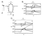
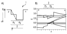
ci<ci+1 かつ ci+1>ci+2
ここでは、成長方向に対して平行に、p端子側からn端子側へ順番に連続番号が前記ゾーンに付与される。有利にはi=1である。換言すると、活性量子井戸は中央に、インジウム含有率が高い中央ゾーンを有し、該中央ゾーンの両側に、それよりインジウム含有率が低いゾーンが設けられている。
ci>ci+1 かつ ci+2>ci+1 かつ ci>ci+2
換言すると、i+1番目のゾーンは、インジウム含有率がより高い2つのゾーンに挟まれる。i+1番目のゾーンはたとえば、量子井戸の分布プロフィールにおいて中間バリアとなる。有利には、i=1またはi=2である。
wi>wi+1 かつ wi+2>wi+1
換言すると、幅が大きい2つのゾーン間に、幅がより小さいゾーンが設けられる。この実施例では、とりわけi+1番目のゾーンは、活性量子井戸のゾーンのうち最大平均インジウム含有率を有するゾーンである。すなわち、有利にはi=1またはi=2である。
wi<wi+1 かつ wi<wi+2
この実施形態では有利には、i+1番目のゾーンが、最大インジウム含有率を有するゾーンである。したがって、有利にはi=1である。さらに、とりわけwi+1>wi+2を適用することができる。
0.35ci−1≦ci≦0.65ci−1
を適用し、とりわけ、
0.40ci−1≦ci≦0.60ci−1
を適用する。上記両関係式では、有利にはi=2またはi>2である。
Eg(x)=x・3.42+(1−x)・0.77−x・(1−x)・1.43
によって表すことができる。ここでは、Applied Physics Letters, Vol. 80, Issue 25, 2002年度、第4741〜4743頁を参照されたい。
Claims (15)
- 窒化物材料系をベースとするオプトエレクトロニクス半導体チップであって、
前記オプトエレクトロニクス半導体チップ(1)は少なくとも1つの活性量子井戸(2)を有し、
動作中、前記活性量子井戸(2)において電磁波が生成され、
前記活性量子井戸(2)は、前記オプトエレクトロニクス半導体チップ(1)の成長方向zに対して平行な方向に、相互に重なったN個のゾーン(A)を有し、ただし、Nは2以上の自然数であり、
前記ゾーン(A)のうち少なくとも2つのゾーンの平均インジウム含有率cは相互に異なり、
前記活性量子井戸(2)は、条件
- 前記活性量子井戸(2)は、条件
ciはi番目の前記ゾーン(A)の平均インジウム含有率であり、
wiは前記i番目のゾーン(A)の幅である、
請求項1記載のオプトエレクトロニクス半導体チップ。 - 前記活性量子井戸(2)の前記ゾーン(A)の各インジウム含有率cは一定である、請求項1または2記載のオプトエレクトロニクス半導体チップ。
- N≧3であり、
前記ゾーン(A)に、前記成長方向zに平行な方向に順に連続番号を付した場合、該成長方向zに対して平行に前記半導体チップ(1)のp端子側(p)からn端子側(n)に向かう方向における前記ゾーン(A)の少なくとも一部の平均インジウム含有率に、
ci<ci+1 かつci+1>ci+2
が適用される、請求項1から3までのいずれか1項記載のオプトエレクトロニクス半導体チップ。 - ci<ci+2である、請求項4記載のオプトエレクトロニクス半導体チップ。
- N≧3であり、
前記ゾーン(A)に、前記成長方向zに平行な方向に順に連続番号を付した場合、該成長方向zに対して平行に前記半導体チップ(1)のp端子側(p)からn端子側(n)に向かう方向における前記ゾーン(A)の少なくとも一部の平均インジウム含有率に、
ci>ci+1 かつci+1>ci+2 かつci>ci+2
が適用される、請求項1から5までのいずれか1項記載のオプトエレクトロニクス半導体チップ。 - 前記活性量子井戸(2)の前記インジウム含有率cは、前記成長方向zに対して平行な方向に単調に増大していく、請求項1から3までのいずれか1項記載のオプトエレクトロニクス半導体チップ。
- Nは3〜10であり、
前記活性量子井戸(2)の全幅(W)は0.25nm〜12nmである、請求項1から7までのいずれか1項記載のオプトエレクトロニクス半導体チップ。 - 前記活性量子井戸(2)は、前記成長方向zに対して平行な方向に2〜5個である、請求項1から8までのいずれか1項記載のオプトエレクトロニクス半導体チップ。
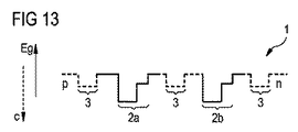
- 前記オプトエレクトロニクス半導体チップ(1)は少なくとも2つの非活性量子井戸(3)を有し、
前記非活性量子井戸(3)の各インジウム含有率は、前記活性量子井戸(2)の最大インジウム含有率より小さい、請求項1から9までのいずれか1項記載のオプトエレクトロニクス半導体チップ。 - 少なくとも2つの隣接する前記活性量子井戸(2)間に、前記非活性量子井戸(3)が少なくとも1つ設けられている、請求項9および10記載のオプトエレクトロニクス半導体チップ。
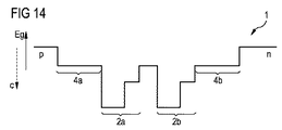
- 前記オプトエレクトロニクス半導体チップ(1)は少なくとも2つの導波層(4)を含み、前記活性量子井戸(2)は該導波層(4)間に設けられており、
前記導波層(4)のうち少なくとも1つの導波層は、少なくとも1つのキャリア障壁層(5)を含む、請求項1から11までのいずれか1項記載のオプトエレクトロニクス半導体チップ。 - 前記オプトエレクトロニクス半導体チップ(1)はレーザ光を生成するために構成されている、請求項1から12までのいずれか1項記載のオプトエレクトロニクス半導体チップ。
- 前記オプトエレクトロニクス半導体チップ(1)は、430nm〜540nmの電磁波を生成するために構成されている、請求項1から13までのいずれか1項記載のオプトエレクトロニクス半導体チップ。
- 窒化物材料系をベースとするオプトエレクトロニクス半導体チップであって、
前記オプトエレクトロニクス半導体チップ(1)は少なくとも1つの活性量子井戸(2)を有し、
動作中、前記活性量子井戸(2)において電磁波が生成され、
前記活性量子井戸(2)は、前記オプトエレクトロニクス半導体チップ(1)の成長方向zに対して平行な方向に、相互に重なったN個のゾーン(A)を有し、ただし、Nは2以上の自然数であり、
前記ゾーン(A)には、前記成長方向zに対して平行な方向に順に連続番号が付されており、
前記ゾーン(A)のうち少なくとも2つのゾーンの平均アルミニウム含有率kは相互に異なり、
前記活性量子井戸(2)は、
Applications Claiming Priority (3)
| Application Number | Priority Date | Filing Date | Title |
|---|---|---|---|
| DE102009015569.4 | 2009-03-30 | ||
| DE102009015569.4A DE102009015569B9 (de) | 2009-03-30 | 2009-03-30 | Optoelektronischer Halbleiterchip |
| PCT/EP2010/053047 WO2010112310A1 (de) | 2009-03-30 | 2010-03-10 | Optoelektronischer halbleiterchip |
Related Child Applications (1)
| Application Number | Title | Priority Date | Filing Date |
|---|---|---|---|
| JP2015025476A Division JP5933775B2 (ja) | 2009-03-30 | 2015-02-12 | オプトエレクトロニクス半導体チップ |
Publications (2)
| Publication Number | Publication Date |
|---|---|
| JP2012522390A true JP2012522390A (ja) | 2012-09-20 |
| JP2012522390A5 JP2012522390A5 (ja) | 2013-03-28 |
Family
ID=42340450
Family Applications (3)
| Application Number | Title | Priority Date | Filing Date |
|---|---|---|---|
| JP2012502545A Pending JP2012522390A (ja) | 2009-03-30 | 2010-03-10 | オプトエレクトロニクス半導体チップ |
| JP2015025476A Active JP5933775B2 (ja) | 2009-03-30 | 2015-02-12 | オプトエレクトロニクス半導体チップ |
| JP2016092753A Pending JP2016157977A (ja) | 2009-03-30 | 2016-05-02 | オプトエレクトロニクス半導体チップ |
Family Applications After (2)
| Application Number | Title | Priority Date | Filing Date |
|---|---|---|---|
| JP2015025476A Active JP5933775B2 (ja) | 2009-03-30 | 2015-02-12 | オプトエレクトロニクス半導体チップ |
| JP2016092753A Pending JP2016157977A (ja) | 2009-03-30 | 2016-05-02 | オプトエレクトロニクス半導体チップ |
Country Status (8)
| Country | Link |
|---|---|
| US (2) | US8908733B2 (ja) |
| EP (1) | EP2415085B1 (ja) |
| JP (3) | JP2012522390A (ja) |
| KR (2) | KR101645057B1 (ja) |
| CN (2) | CN104319331B (ja) |
| DE (1) | DE102009015569B9 (ja) |
| TW (1) | TWI452723B (ja) |
| WO (1) | WO2010112310A1 (ja) |
Cited By (4)
| Publication number | Priority date | Publication date | Assignee | Title |
|---|---|---|---|---|
| JP2015043352A (ja) * | 2013-08-24 | 2015-03-05 | 日亜化学工業株式会社 | 半導体発光素子 |
| JP2015092636A (ja) * | 2009-03-30 | 2015-05-14 | オスラム オプト セミコンダクターズ ゲゼルシャフト ミット ベシュレンクテル ハフツングOsram Opto Semiconductors GmbH | オプトエレクトロニクス半導体チップ |
| JP2019525474A (ja) * | 2016-09-16 | 2019-09-05 | オスラム オプト セミコンダクターズ ゲゼルシャフト ミット ベシュレンクテル ハフツングOsram Opto Semiconductors GmbH | 半導体積層体 |
| JP2020068311A (ja) * | 2018-10-25 | 2020-04-30 | 日亜化学工業株式会社 | 発光素子 |
Families Citing this family (12)
| Publication number | Priority date | Publication date | Assignee | Title |
|---|---|---|---|---|
| KR101712049B1 (ko) | 2010-11-17 | 2017-03-03 | 엘지이노텍 주식회사 | 발광 소자 |
| JP5417307B2 (ja) * | 2010-12-02 | 2014-02-12 | 株式会社東芝 | 半導体発光素子 |
| JP2014067893A (ja) * | 2012-09-26 | 2014-04-17 | Toyoda Gosei Co Ltd | Iii族窒化物半導体発光素子 |
| DE102013200507A1 (de) * | 2013-01-15 | 2014-07-17 | Osram Opto Semiconductors Gmbh | Optoelektronisches Halbleiterbauelement |
| DE102013104351B4 (de) | 2013-04-29 | 2022-01-20 | OSRAM Opto Semiconductors Gesellschaft mit beschränkter Haftung | Halbleiterschichtenfolge und Verfahren zum Betreiben eines optoelektronischen Halbleiterchips |
| JP2015038949A (ja) * | 2013-07-17 | 2015-02-26 | 株式会社東芝 | 半導体発光素子及びその製造方法 |
| KR102019858B1 (ko) * | 2013-07-18 | 2019-09-09 | 엘지이노텍 주식회사 | 발광소자 및 조명시스템 |
| FR3009894B1 (fr) | 2013-08-22 | 2016-12-30 | Commissariat Energie Atomique | Diode electroluminescente dont une zone active comporte des couches d'inn |
| CN108463930B (zh) * | 2016-01-08 | 2020-05-12 | 索尼公司 | 半导体发光器件、显示单元和电子设备 |
| JP7295371B2 (ja) | 2018-08-31 | 2023-06-21 | 日亜化学工業株式会社 | 半導体レーザ素子 |
| US10735354B1 (en) | 2018-10-30 | 2020-08-04 | Facebook, Inc. | Photo space user interface facilitating contextual discussion between users of a social networking system |
| FR3096508A1 (fr) * | 2019-05-21 | 2020-11-27 | Aledia | Dispositif optoélectronique à diodes électroluminescentes |
Citations (6)
| Publication number | Priority date | Publication date | Assignee | Title |
|---|---|---|---|---|
| JP2002368343A (ja) * | 2001-06-05 | 2002-12-20 | Sony Corp | 窒化物半導体レーザ |
| JP2003273473A (ja) * | 2001-11-05 | 2003-09-26 | Nichia Chem Ind Ltd | 半導体素子 |
| JP2005012216A (ja) * | 2003-06-18 | 2005-01-13 | Lumileds Lighting Us Llc | Iii族窒化物発光デバイスのためのヘテロ構造 |
| WO2005020396A1 (ja) * | 2003-08-26 | 2005-03-03 | Sony Corporation | GaN系III−V族化合物半導体発光素子及びその製造方法 |
| JP2007067418A (ja) * | 2005-08-24 | 2007-03-15 | Philips Lumileds Lightng Co Llc | 二重ヘテロ構造の発光領域を有するiii族窒化物発光デバイス |
| JP2007515791A (ja) * | 2004-08-13 | 2007-06-14 | ソウル ナショナル ユニヴァーシティー インダストリー ファンデーション | 窒化物半導体層を成長させる方法及びこれを利用する窒化物半導体発光素子 |
Family Cites Families (17)
| Publication number | Priority date | Publication date | Assignee | Title |
|---|---|---|---|---|
| KR950000119B1 (ko) * | 1991-12-30 | 1995-01-09 | 주식회사 금성사 | 반도체 레이저의 구조 |
| JP3543498B2 (ja) * | 1996-06-28 | 2004-07-14 | 豊田合成株式会社 | 3族窒化物半導体発光素子 |
| DE19955747A1 (de) | 1999-11-19 | 2001-05-23 | Osram Opto Semiconductors Gmbh | Optische Halbleitervorrichtung mit Mehrfach-Quantentopf-Struktur |
| US6618413B2 (en) * | 2001-12-21 | 2003-09-09 | Xerox Corporation | Graded semiconductor layers for reducing threshold voltage for a nitride-based laser diode structure |
| JP2003229645A (ja) | 2002-01-31 | 2003-08-15 | Nec Corp | 量子井戸構造およびそれを用いた半導体素子ならびに半導体素子の製造方法 |
| JP4047150B2 (ja) * | 2002-11-28 | 2008-02-13 | ローム株式会社 | 半導体発光素子 |
| JP4412918B2 (ja) | 2003-05-28 | 2010-02-10 | シャープ株式会社 | 窒化物半導体発光素子及びその製造方法 |
| JP2004356356A (ja) | 2003-05-29 | 2004-12-16 | Oki Electric Ind Co Ltd | 洗浄終了判定方法および洗浄装置 |
| US7138648B2 (en) | 2003-12-17 | 2006-11-21 | Palo Alto Research Center Incorporated | Ultraviolet group III-nitride-based quantum well laser diodes |
| DE102005035722B9 (de) * | 2005-07-29 | 2021-11-18 | OSRAM Opto Semiconductors Gesellschaft mit beschränkter Haftung | Optoelektronischer Halbleiterchip und Verfahren zu dessen Herstellung |
| JP5244297B2 (ja) * | 2006-04-12 | 2013-07-24 | 株式会社日立製作所 | 半導体発光素子 |
| JP2008288397A (ja) * | 2007-05-17 | 2008-11-27 | Eudyna Devices Inc | 半導体発光装置 |
| KR101459752B1 (ko) * | 2007-06-22 | 2014-11-13 | 엘지이노텍 주식회사 | 반도체 발광소자 및 그 제조방법 |
| DE102007044439B4 (de) * | 2007-09-18 | 2022-03-24 | OSRAM Opto Semiconductors Gesellschaft mit beschränkter Haftung | Optoelektronischer Halbleiterchip mit Quantentopfstruktur |
| JP5281162B2 (ja) * | 2008-09-03 | 2013-09-04 | テレフオンアクチーボラゲット エル エム エリクソン(パブル) | 通信帯域を割当てるための方法及び関連する装置 |
| DE102009015569B9 (de) * | 2009-03-30 | 2023-06-29 | OSRAM Opto Semiconductors Gesellschaft mit beschränkter Haftung | Optoelektronischer Halbleiterchip |
| US8779412B2 (en) * | 2011-07-20 | 2014-07-15 | Samsung Electronics Co., Ltd. | Semiconductor light emitting device |
-
2009
- 2009-03-30 DE DE102009015569.4A patent/DE102009015569B9/de active Active
-
2010
- 2010-03-10 KR KR1020117025789A patent/KR101645057B1/ko active IP Right Grant
- 2010-03-10 WO PCT/EP2010/053047 patent/WO2010112310A1/de active Application Filing
- 2010-03-10 KR KR1020167017756A patent/KR101704985B1/ko active IP Right Grant
- 2010-03-10 CN CN201410437730.8A patent/CN104319331B/zh active Active
- 2010-03-10 US US13/262,583 patent/US8908733B2/en active Active
- 2010-03-10 CN CN201080014639.5A patent/CN102369606B/zh active Active
- 2010-03-10 JP JP2012502545A patent/JP2012522390A/ja active Pending
- 2010-03-10 EP EP10707304.1A patent/EP2415085B1/de active Active
- 2010-03-25 TW TW099108846A patent/TWI452723B/zh active
-
2014
- 2014-11-06 US US14/535,044 patent/US9202971B2/en active Active
-
2015
- 2015-02-12 JP JP2015025476A patent/JP5933775B2/ja active Active
-
2016
- 2016-05-02 JP JP2016092753A patent/JP2016157977A/ja active Pending
Patent Citations (6)
| Publication number | Priority date | Publication date | Assignee | Title |
|---|---|---|---|---|
| JP2002368343A (ja) * | 2001-06-05 | 2002-12-20 | Sony Corp | 窒化物半導体レーザ |
| JP2003273473A (ja) * | 2001-11-05 | 2003-09-26 | Nichia Chem Ind Ltd | 半導体素子 |
| JP2005012216A (ja) * | 2003-06-18 | 2005-01-13 | Lumileds Lighting Us Llc | Iii族窒化物発光デバイスのためのヘテロ構造 |
| WO2005020396A1 (ja) * | 2003-08-26 | 2005-03-03 | Sony Corporation | GaN系III−V族化合物半導体発光素子及びその製造方法 |
| JP2007515791A (ja) * | 2004-08-13 | 2007-06-14 | ソウル ナショナル ユニヴァーシティー インダストリー ファンデーション | 窒化物半導体層を成長させる方法及びこれを利用する窒化物半導体発光素子 |
| JP2007067418A (ja) * | 2005-08-24 | 2007-03-15 | Philips Lumileds Lightng Co Llc | 二重ヘテロ構造の発光領域を有するiii族窒化物発光デバイス |
Cited By (6)
| Publication number | Priority date | Publication date | Assignee | Title |
|---|---|---|---|---|
| JP2015092636A (ja) * | 2009-03-30 | 2015-05-14 | オスラム オプト セミコンダクターズ ゲゼルシャフト ミット ベシュレンクテル ハフツングOsram Opto Semiconductors GmbH | オプトエレクトロニクス半導体チップ |
| JP2015043352A (ja) * | 2013-08-24 | 2015-03-05 | 日亜化学工業株式会社 | 半導体発光素子 |
| US9912123B2 (en) | 2013-08-24 | 2018-03-06 | Nichia Corporation | Semiconductor light emitting device |
| JP2019525474A (ja) * | 2016-09-16 | 2019-09-05 | オスラム オプト セミコンダクターズ ゲゼルシャフト ミット ベシュレンクテル ハフツングOsram Opto Semiconductors GmbH | 半導体積層体 |
| US10720549B2 (en) | 2016-09-16 | 2020-07-21 | Osram Oled Gmbh | Semiconductor layer sequence having pre- and post-barrier layers and quantum wells |
| JP2020068311A (ja) * | 2018-10-25 | 2020-04-30 | 日亜化学工業株式会社 | 発光素子 |
Also Published As
| Publication number | Publication date |
|---|---|
| CN104319331B (zh) | 2017-05-10 |
| JP2016157977A (ja) | 2016-09-01 |
| EP2415085A1 (de) | 2012-02-08 |
| DE102009015569A1 (de) | 2010-10-07 |
| KR20160085909A (ko) | 2016-07-18 |
| DE102009015569B4 (de) | 2023-03-23 |
| US20150063395A1 (en) | 2015-03-05 |
| CN102369606A (zh) | 2012-03-07 |
| JP5933775B2 (ja) | 2016-06-15 |
| KR20120009475A (ko) | 2012-01-31 |
| CN102369606B (zh) | 2014-10-01 |
| KR101645057B1 (ko) | 2016-08-02 |
| DE102009015569B9 (de) | 2023-06-29 |
| US20130028281A1 (en) | 2013-01-31 |
| WO2010112310A1 (de) | 2010-10-07 |
| JP2015092636A (ja) | 2015-05-14 |
| KR101704985B1 (ko) | 2017-02-08 |
| TW201044635A (en) | 2010-12-16 |
| EP2415085B1 (de) | 2019-01-02 |
| US8908733B2 (en) | 2014-12-09 |
| US9202971B2 (en) | 2015-12-01 |
| TWI452723B (zh) | 2014-09-11 |
| CN104319331A (zh) | 2015-01-28 |
Similar Documents
| Publication | Publication Date | Title |
|---|---|---|
| JP5933775B2 (ja) | オプトエレクトロニクス半導体チップ | |
| JP6327323B2 (ja) | 半導体レーザ素子及びその製造方法 | |
| JP5795010B2 (ja) | オプトエレクトロニクス半導体チップ | |
| US10522699B2 (en) | Optoelectronic semiconductor chip | |
| KR20190025706A (ko) | 반도체 층 시퀀스 | |
| JP2004320038A (ja) | 量子井戸の有効キャリヤ捕獲断面積を増大させるための要素を有する発光素子 | |
| JP6564348B2 (ja) | 深紫外発光素子 | |
| JP2020115539A (ja) | 半導体レーザ素子 | |
| JP2014112654A (ja) | 窒化物半導体面発光レーザ及びその製造方法 | |
| WO2014061174A1 (ja) | 半導体発光素子 | |
| CN111937261B (zh) | 半导体发光元件 | |
| JP2008506257A (ja) | 発光素子の最大変調速度を改善する方法及び最大変調速度の改善された発光素子、並びにその量子井戸構造 | |
| JP2018200928A (ja) | 半導体レーザ素子 | |
| WO2018163824A1 (ja) | 半導体発光素子および半導体発光素子の製造方法 | |
| US20200313039A1 (en) | Light emitting device and projector | |
| CN110875576B (zh) | 半导体激光元件 | |
| WO2023042675A1 (ja) | 垂直共振器型発光素子 | |
| US9106053B2 (en) | Distributed feedback surface emitting laser | |
| JP6159642B2 (ja) | 発光素子 | |
| US8143615B2 (en) | Electron beam emitting device with a superlattice structure | |
| CN111446621B (zh) | 半导体激光元件及其制造方法 | |
| JP6829235B2 (ja) | 半導体発光素子および半導体発光素子の製造方法 | |
| WO2024084898A1 (ja) | 垂直共振器型発光素子 | |
| JP2024058791A (ja) | 垂直共振器型発光素子 | |
| CN114976867A (zh) | 发光装置及投影仪 |
Legal Events
| Date | Code | Title | Description |
|---|---|---|---|
| A521 | Request for written amendment filed |
Free format text: JAPANESE INTERMEDIATE CODE: A523 Effective date: 20130206 |
|
| A621 | Written request for application examination |
Free format text: JAPANESE INTERMEDIATE CODE: A621 Effective date: 20130206 |
|
| A977 | Report on retrieval |
Free format text: JAPANESE INTERMEDIATE CODE: A971007 Effective date: 20140127 |
|
| A131 | Notification of reasons for refusal |
Free format text: JAPANESE INTERMEDIATE CODE: A131 Effective date: 20140203 |
|
| A521 | Request for written amendment filed |
Free format text: JAPANESE INTERMEDIATE CODE: A523 Effective date: 20140502 |
|
| A02 | Decision of refusal |
Free format text: JAPANESE INTERMEDIATE CODE: A02 Effective date: 20141014 |