JP2012251031A - リフレクタ材料および発光ダイオード装置 - Google Patents
リフレクタ材料および発光ダイオード装置 Download PDFInfo
- Publication number
- JP2012251031A JP2012251031A JP2011123217A JP2011123217A JP2012251031A JP 2012251031 A JP2012251031 A JP 2012251031A JP 2011123217 A JP2011123217 A JP 2011123217A JP 2011123217 A JP2011123217 A JP 2011123217A JP 2012251031 A JP2012251031 A JP 2012251031A
- Authority
- JP
- Japan
- Prior art keywords
- group
- reflector
- emitting diode
- light
- light emitting
- Prior art date
- Legal status (The legal status is an assumption and is not a legal conclusion. Google has not performed a legal analysis and makes no representation as to the accuracy of the status listed.)
- Granted
Links
Images


Classifications
-
- H—ELECTRICITY
- H10—SEMICONDUCTOR DEVICES; ELECTRIC SOLID-STATE DEVICES NOT OTHERWISE PROVIDED FOR
- H10H—INORGANIC LIGHT-EMITTING SEMICONDUCTOR DEVICES HAVING POTENTIAL BARRIERS
- H10H20/00—Individual inorganic light-emitting semiconductor devices having potential barriers, e.g. light-emitting diodes [LED]
- H10H20/80—Constructional details
- H10H20/85—Packages
- H10H20/855—Optical field-shaping means, e.g. lenses
- H10H20/856—Reflecting means
-
- H—ELECTRICITY
- H01—ELECTRIC ELEMENTS
- H01L—SEMICONDUCTOR DEVICES NOT COVERED BY CLASS H10
- H01L24/00—Arrangements for connecting or disconnecting semiconductor or solid-state bodies; Methods or apparatus related thereto
- H01L24/93—Batch processes
- H01L24/95—Batch processes at chip-level, i.e. with connecting carried out on a plurality of singulated devices, i.e. on diced chips
- H01L24/97—Batch processes at chip-level, i.e. with connecting carried out on a plurality of singulated devices, i.e. on diced chips the devices being connected to a common substrate, e.g. interposer, said common substrate being separable into individual assemblies after connecting
-
- H—ELECTRICITY
- H01—ELECTRIC ELEMENTS
- H01L—SEMICONDUCTOR DEVICES NOT COVERED BY CLASS H10
- H01L2224/00—Indexing scheme for arrangements for connecting or disconnecting semiconductor or solid-state bodies and methods related thereto as covered by H01L24/00
- H01L2224/01—Means for bonding being attached to, or being formed on, the surface to be connected, e.g. chip-to-package, die-attach, "first-level" interconnects; Manufacturing methods related thereto
- H01L2224/10—Bump connectors; Manufacturing methods related thereto
- H01L2224/15—Structure, shape, material or disposition of the bump connectors after the connecting process
- H01L2224/16—Structure, shape, material or disposition of the bump connectors after the connecting process of an individual bump connector
- H01L2224/161—Disposition
- H01L2224/16151—Disposition the bump connector connecting between a semiconductor or solid-state body and an item not being a semiconductor or solid-state body, e.g. chip-to-substrate, chip-to-passive
- H01L2224/16221—Disposition the bump connector connecting between a semiconductor or solid-state body and an item not being a semiconductor or solid-state body, e.g. chip-to-substrate, chip-to-passive the body and the item being stacked
- H01L2224/16225—Disposition the bump connector connecting between a semiconductor or solid-state body and an item not being a semiconductor or solid-state body, e.g. chip-to-substrate, chip-to-passive the body and the item being stacked the item being non-metallic, e.g. insulating substrate with or without metallisation
-
- H—ELECTRICITY
- H01—ELECTRIC ELEMENTS
- H01L—SEMICONDUCTOR DEVICES NOT COVERED BY CLASS H10
- H01L2924/00—Indexing scheme for arrangements or methods for connecting or disconnecting semiconductor or solid-state bodies as covered by H01L24/00
- H01L2924/10—Details of semiconductor or other solid state devices to be connected
- H01L2924/11—Device type
- H01L2924/12—Passive devices, e.g. 2 terminal devices
- H01L2924/1204—Optical Diode
- H01L2924/12041—LED
-
- H—ELECTRICITY
- H01—ELECTRIC ELEMENTS
- H01L—SEMICONDUCTOR DEVICES NOT COVERED BY CLASS H10
- H01L2924/00—Indexing scheme for arrangements or methods for connecting or disconnecting semiconductor or solid-state bodies as covered by H01L24/00
- H01L2924/10—Details of semiconductor or other solid state devices to be connected
- H01L2924/11—Device type
- H01L2924/12—Passive devices, e.g. 2 terminal devices
- H01L2924/1204—Optical Diode
- H01L2924/12042—LASER
-
- H—ELECTRICITY
- H01—ELECTRIC ELEMENTS
- H01L—SEMICONDUCTOR DEVICES NOT COVERED BY CLASS H10
- H01L2924/00—Indexing scheme for arrangements or methods for connecting or disconnecting semiconductor or solid-state bodies as covered by H01L24/00
- H01L2924/15—Details of package parts other than the semiconductor or other solid state devices to be connected
- H01L2924/151—Die mounting substrate
- H01L2924/156—Material
- H01L2924/15786—Material with a principal constituent of the material being a non metallic, non metalloid inorganic material
- H01L2924/15787—Ceramics, e.g. crystalline carbides, nitrides or oxides
-
- H—ELECTRICITY
- H01—ELECTRIC ELEMENTS
- H01L—SEMICONDUCTOR DEVICES NOT COVERED BY CLASS H10
- H01L2924/00—Indexing scheme for arrangements or methods for connecting or disconnecting semiconductor or solid-state bodies as covered by H01L24/00
- H01L2924/15—Details of package parts other than the semiconductor or other solid state devices to be connected
- H01L2924/181—Encapsulation
-
- H—ELECTRICITY
- H10—SEMICONDUCTOR DEVICES; ELECTRIC SOLID-STATE DEVICES NOT OTHERWISE PROVIDED FOR
- H10H—INORGANIC LIGHT-EMITTING SEMICONDUCTOR DEVICES HAVING POTENTIAL BARRIERS
- H10H20/00—Individual inorganic light-emitting semiconductor devices having potential barriers, e.g. light-emitting diodes [LED]
- H10H20/01—Manufacture or treatment
- H10H20/036—Manufacture or treatment of packages
- H10H20/0363—Manufacture or treatment of packages of optical field-shaping means
Landscapes
- Engineering & Computer Science (AREA)
- Computer Hardware Design (AREA)
- Microelectronics & Electronic Packaging (AREA)
- Power Engineering (AREA)
- Led Device Packages (AREA)
- Compositions Of Macromolecular Compounds (AREA)
- Silicon Polymers (AREA)
Abstract
【解決手段】シラノール基両末端ポリシロキサンと、エチレン系ケイ素化合物と、エポキシ基含有ケイ素化合物と、オルガノハイドロジェンシロキサンと、縮合触媒と、付加触媒とから調製されるシリコーン樹脂組成物と、光反射成分とを含有することをリフレクタ材料から形成されるリフレクタ4を発光ダイオード装置1に設ける。
【選択図】図1
Description
一般式(1):
上記一般式(1)中、R1で示される1価の炭化水素基において、飽和炭化水素基としては、例えば、炭素数1〜6の直鎖状または分岐状のアルキル基(メチル基、エチル基、プロピル基、イソプロピル基、ブチル基、イソブチル基、ペンチル基、ヘキシル基など)、例えば、炭素数3〜6のシクロアルキル基(シクロペンチル基、シクロヘキシル基など)などが挙げられる。
一般式(2):
R2−Si(X1)3 (2)
(一般式(2)中、R2は、1価のエチレン系不飽和炭化水素基を示し、X1は、ハロゲン原子、アルコキシ基、フェノキシ基、またはアセトキシ基を示す。但し、X1は、同一または互いに相異なっていてもよい。)
上記一般式(2)において、R2で示されるエチレン系不飽和炭化水素基としては、置換または非置換のエチレン系不飽和炭化水素基が挙げられ、例えば、アルケニル基、シクロアルケニル基などが挙げられる。
一般式(3):
R3−Si(X2)3 (3)
(一般式(3)中、R3は、エポキシ構造含有基を示し、X2は、ハロゲン原子、アルコキシ基、フェノキシ基、またはアセトキシ基を示す。但し、X2は、同一または互いに相異なっていてもよい。)
一般式(3)において、R3で示されるエポキシ構造含有基としては、例えば、エポキシ基、例えば、グリシジルエーテル基、例えば、エポキシシクロヘキシル基などのエポキシシクロアルキル基などが挙げられる。
一般式(4):
上記一般式(4)中、R4で示される2価の炭化水素基において、飽和炭化水素基としては、例えば、炭素数1〜6のアルキレン基(メチレン基、エチレン基、プロピレン基、ブチレン基など)、例えば、炭素数3〜8のシクロアルキレン基(シクロペンチレン基、シクロヘキシレン基など)などが挙げられる。
A〜Dは、水素側鎖含有オルガノポリシロキサンを構成する。
R6で示される1価の炭化水素基において、飽和炭化水素基および芳香族炭化水素基は、上記式(1)のR1で例示した飽和炭化水素基および芳香族炭化水素基と同様のものが挙げられる。1価の炭化水素基として、好ましくは、メチル、フェニル、さらに好ましくは、メチルが挙げられる。
シラノール基両末端ポリジメチルシロキサン(シラノール基両末端ポリシロキサン)(式(1)中、R1がすべてメチル基、nの平均が115、数平均分子量11500)100.0g(8.70mmol)と、ビニルトリメトキシシラン(エチレン系ケイ素化合物)(式(2)中、R2がビニル基、X1がすべてメトキシ基)0.77g(5.20mmol)と、(3−グリシドキシプロピル)トリメトキシシラン(エポキシ基含有ケイ素化合物)(式(3)中、R3が3−グリシドキシプロピル基、X2がすべてメトキシ基)0.14g(0.59mmol)と、水酸化テトラメチルアンモニウム(縮合触媒)の10質量%メタノール溶液47.5μL(水酸化テトラメチルアンモニウム量:0.04mmol)を配合して、室温(25℃)で、1時間攪拌することにより混合物を得た。
シリコーン樹脂組成物、酸化チタンおよびシリカの配合割合を表1に準拠して変更した以外は、実施例1と同様に処理して、リフレクタ材料を得、その後、試験片を得た。
下記に示す各成分を表1に示す配合割合で配合し、ビーカー中で溶融混合し、熟成した後、室温まで冷却して粉砕することにより粉末状のエポキシ樹脂組成物を調製した。
1、3、5−トリスグリシジルイソシアヌル酸(エポキシ樹脂、エポキシ当量100g/Eq)
メチルヘキサヒドロキシ無水フタル酸(酸無水物、酸当量168g/Eq)
酸化チタン(ルチル型、平均粒径0.2μm)
シリカ(無機充填剤、平均粒径23μm)、
9、10−ジヒドロ−9−オキサ−10−ホスファフェナンスレン−10−オキサイド(酸化防止剤)
テトラ−n−ブチルホスホニウム−o、o−ジエチルホスホロンジチオエート(硬化促進剤)
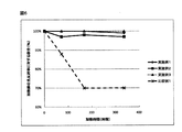
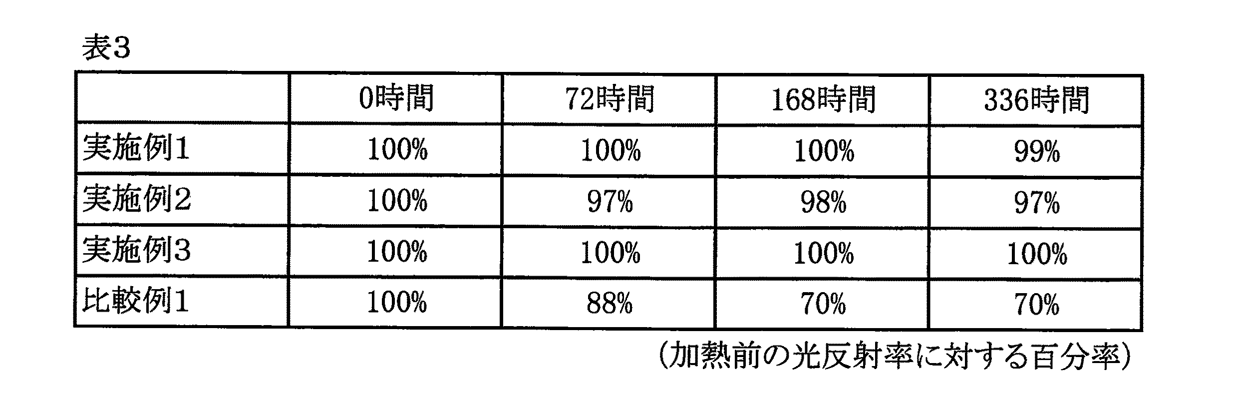
1. 耐熱性(光透過率の減少率)
実施例1〜3および比較例1の試験片について、室温(25℃)において、波長380〜800nmの光に対する光反射率を分光光度計(U−670、日本分光社製)にて測定し、試験片の面方向全領域に渡り80%以上を保持しているか確認した。
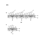
2 基板
3 発光ダイオード素子
4 リフレクタ
4A リフレクタ前駆体
A〜Dは、水素側鎖含有オルガノポリシロキサンを構成する。
R6で示される1価の炭化水素基において、飽和炭化水素基および芳香族炭化水素基は、上記式(1)のR1で例示した飽和炭化水素基および芳香族炭化水素基と同様のものが挙げられる。1価の炭化水素基として、好ましくは、メチル、フェニル、さらに好ましくは、メチルが挙げられる。
下記に示す各成分を表2に示す配合割合で配合し、ビーカー中で溶融混合し、熟成した後、室温まで冷却して粉砕することにより粉末状のエポキシ樹脂組成物を調製した。
1,3,5−トリスグリシジルイソシアヌル酸(エポキシ樹脂、エポキシ当量100g/Eq)
メチルヘキサヒドロキシ無水フタル酸(酸無水物、酸当量168g/Eq)
酸化チタン(ルチル型、平均粒径0.2μm)
シリカ(無機充填剤、平均粒径23μm)、
9、10−ジヒドロ−9−オキサ−10−ホスファフェナンスレン−10−オキサイド(酸化防止剤)
テトラ−n−ブチルホスホニウム−o,o−ジエチルホスホロンジチオエート(硬化促進剤)
Claims (9)
- シラノール基両末端ポリシロキサン、エチレン系ケイ素化合物、エポキシ基含有ケイ素化合物、オルガノハイドロジェンシロキサン、縮合触媒および付加触媒から調製されるシリコーン樹脂組成物と、
光反射成分と
を含有することを特徴とする、リフレクタ材料。 - 前記光反射成分が、白色顔料であることを特徴とする、請求項1に記載のリフレクタ材料。
- 前記光反射成分が、酸化チタンであることを特徴とする、請求項1または2に記載のリフレクタ材料。
- 前記光反射成分が、ルチル型結晶構造を有する酸化チタンであることを特徴とする、請求項1〜3のいずれか一項に記載のリフレクタ材料。
- 無機充填剤をさらに含有していることを特徴とする、請求項1〜4のいずれか一項に記載のリフレクタ材料。
- 前記シリコーン樹脂組成物が半硬化状態であることを特徴とする、請求項1〜5のいずれか一項に記載のリフレクタ材料。
- シート形状に形成されていることを特徴とする、請求項6に記載のリフレクタ材料。
- 基板と、
前記基板の上に設けられる発光ダイオード素子と、
前記基板の上に、前記発光ダイオード素子を囲うように設けられ、請求項6または7に記載のリフレクタ材料から形成されるリフレクタと
を備えることを特徴とする、発光ダイオード装置。 - 前記リフレクタは、前記発光ダイオード素子の側面に密着するように設けられることを特徴とする、請求項8に記載の発光ダイオード装置。
Priority Applications (6)
| Application Number | Priority Date | Filing Date | Title |
|---|---|---|---|
| JP2011123217A JP5840388B2 (ja) | 2011-06-01 | 2011-06-01 | 発光ダイオード装置 |
| KR1020120058015A KR20120135071A (ko) | 2011-06-01 | 2012-05-31 | 리플렉터 재료 및 발광 다이오드 장치 |
| EP12170179.1A EP2530752A3 (en) | 2011-06-01 | 2012-05-31 | Reflecting material and light emitting diode device |
| US13/484,399 US8723167B2 (en) | 2011-06-01 | 2012-05-31 | Reflecting material and light emitting diode device |
| TW101119859A TWI478960B (zh) | 2011-06-01 | 2012-06-01 | 反射器材料及發光二極體裝置 |
| CN201210180500.9A CN102807758B (zh) | 2011-06-01 | 2012-06-01 | 反光材料及发光二极管装置 |
Applications Claiming Priority (1)
| Application Number | Priority Date | Filing Date | Title |
|---|---|---|---|
| JP2011123217A JP5840388B2 (ja) | 2011-06-01 | 2011-06-01 | 発光ダイオード装置 |
Related Child Applications (1)
| Application Number | Title | Priority Date | Filing Date |
|---|---|---|---|
| JP2015065980A Division JP2015128188A (ja) | 2015-03-27 | 2015-03-27 | キット |
Publications (2)
| Publication Number | Publication Date |
|---|---|
| JP2012251031A true JP2012251031A (ja) | 2012-12-20 |
| JP5840388B2 JP5840388B2 (ja) | 2016-01-06 |
Family
ID=46318865
Family Applications (1)
| Application Number | Title | Priority Date | Filing Date |
|---|---|---|---|
| JP2011123217A Expired - Fee Related JP5840388B2 (ja) | 2011-06-01 | 2011-06-01 | 発光ダイオード装置 |
Country Status (6)
| Country | Link |
|---|---|
| US (1) | US8723167B2 (ja) |
| EP (1) | EP2530752A3 (ja) |
| JP (1) | JP5840388B2 (ja) |
| KR (1) | KR20120135071A (ja) |
| CN (1) | CN102807758B (ja) |
| TW (1) | TWI478960B (ja) |
Cited By (9)
| Publication number | Priority date | Publication date | Assignee | Title |
|---|---|---|---|---|
| JP2014130918A (ja) * | 2012-12-28 | 2014-07-10 | Nitto Denko Corp | 封止層被覆光半導体素子、その製造方法および光半導体装置 |
| JP2016072379A (ja) * | 2014-09-29 | 2016-05-09 | 日亜化学工業株式会社 | 発光装置及びその製造方法 |
| WO2016148019A1 (ja) * | 2015-03-16 | 2016-09-22 | 日東電工株式会社 | 光反射層付光半導体素子、および、光反射層および蛍光体層付光半導体素子の製造方法 |
| JP2016174148A (ja) * | 2015-03-16 | 2016-09-29 | 日東電工株式会社 | 光反射層付光半導体素子、および、光反射層および蛍光体層付光半導体素子の製造方法 |
| JP2018523310A (ja) * | 2015-07-28 | 2018-08-16 | オスラム オプト セミコンダクターズ ゲゼルシャフト ミット ベシュレンクテル ハフツングOsram Opto Semiconductors GmbH | 構成素子の製造方法および構成素子 |
| JP2019016629A (ja) * | 2017-07-03 | 2019-01-31 | 大日本印刷株式会社 | Ledモジュール |
| JP2019016630A (ja) * | 2017-07-03 | 2019-01-31 | 大日本印刷株式会社 | Ledモジュール |
| JP2019186300A (ja) * | 2018-04-04 | 2019-10-24 | スタンレー電気株式会社 | 半導体発光装置及びその製造方法 |
| JP2020029509A (ja) * | 2018-08-22 | 2020-02-27 | 信越化学工業株式会社 | 白色付加硬化型シリコーン組成物、発光ダイオード用リフレクター及び光半導体装置 |
Families Citing this family (19)
| Publication number | Priority date | Publication date | Assignee | Title |
|---|---|---|---|---|
| JP5670249B2 (ja) * | 2011-04-14 | 2015-02-18 | 日東電工株式会社 | 発光素子転写シートの製造方法、発光装置の製造方法、発光素子転写シートおよび発光装置 |
| US20140001948A1 (en) * | 2012-06-29 | 2014-01-02 | Nitto Denko Corporation | Reflecting layer-phosphor layer-covered led, producing method thereof, led device, and producing method thereof |
| US8907502B2 (en) * | 2012-06-29 | 2014-12-09 | Nitto Denko Corporation | Encapsulating layer-covered semiconductor element, producing method thereof, and semiconductor device |
| US20140009060A1 (en) * | 2012-06-29 | 2014-01-09 | Nitto Denko Corporation | Phosphor layer-covered led, producing method thereof, and led device |
| TWI616489B (zh) * | 2013-02-18 | 2018-03-01 | 可應用於發光二極體元件之聚矽氧烷組合物、基座配方及其發光二極體元件 | |
| US8847261B1 (en) | 2013-03-14 | 2014-09-30 | Cooledge Lighting Inc. | Light-emitting devices having engineered phosphor elements |
| TWI531094B (zh) | 2013-05-17 | 2016-04-21 | Daxin Materials Corp | And a light-emitting device for a light-emitting device |
| JP6186904B2 (ja) | 2013-06-05 | 2017-08-30 | 日亜化学工業株式会社 | 発光装置 |
| US10439111B2 (en) | 2014-05-14 | 2019-10-08 | Genesis Photonics Inc. | Light emitting device and manufacturing method thereof |
| US9997676B2 (en) | 2014-05-14 | 2018-06-12 | Genesis Photonics Inc. | Light emitting device and manufacturing method thereof |
| TWI557952B (zh) | 2014-06-12 | 2016-11-11 | 新世紀光電股份有限公司 | 發光元件 |
| TWI657597B (zh) | 2015-03-18 | 2019-04-21 | 新世紀光電股份有限公司 | 側照式發光二極體結構及其製造方法 |
| WO2016192452A1 (zh) * | 2015-05-29 | 2016-12-08 | 广州市鸿利光电股份有限公司 | Csp led的封装方法和csp led |
| CN106549092A (zh) | 2015-09-18 | 2017-03-29 | 新世纪光电股份有限公司 | 发光装置及其制造方法 |
| CN107968142A (zh) | 2016-10-19 | 2018-04-27 | 新世纪光电股份有限公司 | 发光装置及其制造方法 |
| US10784423B2 (en) | 2017-11-05 | 2020-09-22 | Genesis Photonics Inc. | Light emitting device |
| US11215598B2 (en) | 2019-04-26 | 2022-01-04 | METER Group, Inc. USA | Meat processing sensor suite |
| US20220293574A1 (en) * | 2019-12-03 | 2022-09-15 | Shenzhen Jufei Optoelectronics Co., Ltd. | Led chip module and method for manufacturing led chip module |
| CN112480571A (zh) * | 2020-12-04 | 2021-03-12 | 山东玉马遮阳科技股份有限公司 | 一种珠光pvc材料及其制备方法 |
Citations (7)
| Publication number | Priority date | Publication date | Assignee | Title |
|---|---|---|---|---|
| JP2003209286A (ja) * | 2001-11-08 | 2003-07-25 | Nichia Chem Ind Ltd | 発光装置およびその製造方法 |
| JP2009141322A (ja) * | 2007-08-27 | 2009-06-25 | Avago Technologies Ecbu Ip (Singapore) Pte Ltd | 改良された熱循環耐性を有するled光源 |
| JP2009218274A (ja) * | 2008-03-07 | 2009-09-24 | Stanley Electric Co Ltd | 半導体発光装置 |
| JP2010192629A (ja) * | 2009-02-18 | 2010-09-02 | Nichia Corp | 発光装置の製造方法 |
| JP2010265437A (ja) * | 2009-04-14 | 2010-11-25 | Nitto Denko Corp | 熱硬化性シリコーン樹脂用組成物 |
| JP2010272847A (ja) * | 2009-04-20 | 2010-12-02 | Nichia Corp | 発光装置 |
| JP2011054902A (ja) * | 2009-09-04 | 2011-03-17 | Shin-Etsu Chemical Co Ltd | 光半導体ケース形成用白色熱硬化性シリコーン樹脂組成物及び光半導体ケース |
Family Cites Families (11)
| Publication number | Priority date | Publication date | Assignee | Title |
|---|---|---|---|---|
| JP3420473B2 (ja) * | 1997-04-30 | 2003-06-23 | 東レ・ダウコーニング・シリコーン株式会社 | シリコーン系接着性シート、その製造方法、および半導体装置 |
| KR100405320B1 (ko) * | 2000-12-21 | 2003-11-12 | 제일모직주식회사 | 내충격성 및 광반사율이 우수한 폴리카보네이트계 수지조성물 |
| JP3844196B2 (ja) * | 2001-06-12 | 2006-11-08 | シチズン電子株式会社 | 発光ダイオードの製造方法 |
| DE602007000068D1 (de) * | 2006-02-20 | 2008-09-25 | Shinetsu Chemical Co | Hitzeerhärtbare Silikonzusammensetzung |
| US20090091045A1 (en) | 2006-04-26 | 2009-04-09 | Sekisui Chemical Co., Ltd | Themosetting Composition for Optical Semiconductor, Die Bond Material for Optical Semiconductor Device, Underfill Material for Optical Semiconductor Device, Sealing Agent for Optical Semiconductor Device, and Optical Semiconductor Device |
| CN101432331A (zh) * | 2006-04-26 | 2009-05-13 | 积水化学工业株式会社 | 光半导体用热固化性组合物、光半导体元件用固晶材料、光半导体元件用底填材料、光半导体元件用密封剂及光半导体元件 |
| JP2008202036A (ja) * | 2007-01-22 | 2008-09-04 | Sekisui Chem Co Ltd | 光半導体用熱硬化性組成物、光半導体素子用封止剤、光半導体素子用ダイボンド材、光半導体素子用アンダーフィル材、及び、光半導体素子 |
| WO2009017089A1 (ja) * | 2007-08-01 | 2009-02-05 | Idemitsu Kosan Co., Ltd. | 光反射性ポリカーボネート樹脂組成物及びその成形体 |
| JP5499774B2 (ja) * | 2009-03-04 | 2014-05-21 | 信越化学工業株式会社 | 光半導体封止用組成物及びそれを用いた光半導体装置 |
| US20110049545A1 (en) * | 2009-09-02 | 2011-03-03 | Koninklijke Philips Electronics N.V. | Led package with phosphor plate and reflective substrate |
| JP2011060819A (ja) | 2009-09-07 | 2011-03-24 | Nitto Denko Corp | 光半導体素子収納用実装パッケージ用樹脂組成物およびそれを用いて得られる光半導体発光装置 |
-
2011
- 2011-06-01 JP JP2011123217A patent/JP5840388B2/ja not_active Expired - Fee Related
-
2012
- 2012-05-31 KR KR1020120058015A patent/KR20120135071A/ko not_active Withdrawn
- 2012-05-31 EP EP12170179.1A patent/EP2530752A3/en not_active Withdrawn
- 2012-05-31 US US13/484,399 patent/US8723167B2/en not_active Expired - Fee Related
- 2012-06-01 CN CN201210180500.9A patent/CN102807758B/zh not_active Expired - Fee Related
- 2012-06-01 TW TW101119859A patent/TWI478960B/zh not_active IP Right Cessation
Patent Citations (7)
| Publication number | Priority date | Publication date | Assignee | Title |
|---|---|---|---|---|
| JP2003209286A (ja) * | 2001-11-08 | 2003-07-25 | Nichia Chem Ind Ltd | 発光装置およびその製造方法 |
| JP2009141322A (ja) * | 2007-08-27 | 2009-06-25 | Avago Technologies Ecbu Ip (Singapore) Pte Ltd | 改良された熱循環耐性を有するled光源 |
| JP2009218274A (ja) * | 2008-03-07 | 2009-09-24 | Stanley Electric Co Ltd | 半導体発光装置 |
| JP2010192629A (ja) * | 2009-02-18 | 2010-09-02 | Nichia Corp | 発光装置の製造方法 |
| JP2010265437A (ja) * | 2009-04-14 | 2010-11-25 | Nitto Denko Corp | 熱硬化性シリコーン樹脂用組成物 |
| JP2010272847A (ja) * | 2009-04-20 | 2010-12-02 | Nichia Corp | 発光装置 |
| JP2011054902A (ja) * | 2009-09-04 | 2011-03-17 | Shin-Etsu Chemical Co Ltd | 光半導体ケース形成用白色熱硬化性シリコーン樹脂組成物及び光半導体ケース |
Cited By (16)
| Publication number | Priority date | Publication date | Assignee | Title |
|---|---|---|---|---|
| JP2014130918A (ja) * | 2012-12-28 | 2014-07-10 | Nitto Denko Corp | 封止層被覆光半導体素子、その製造方法および光半導体装置 |
| JP2016072379A (ja) * | 2014-09-29 | 2016-05-09 | 日亜化学工業株式会社 | 発光装置及びその製造方法 |
| US10424703B2 (en) | 2015-03-16 | 2019-09-24 | Epistar Corporation | Method of producing an optical semiconductor device |
| KR20170128298A (ko) * | 2015-03-16 | 2017-11-22 | 닛토덴코 가부시키가이샤 | 광 반사층 부착 광 반도체 소자, 및 광 반사층 및 형광체층 부착 광 반도체 소자의 제조 방법 |
| JP2016174148A (ja) * | 2015-03-16 | 2016-09-29 | 日東電工株式会社 | 光反射層付光半導体素子、および、光反射層および蛍光体層付光半導体素子の製造方法 |
| KR102541533B1 (ko) * | 2015-03-16 | 2023-06-07 | 에피스타 코포레이션 | 광 반사층 부착 광 반도체 소자, 및 광 반사층 및 형광체층 부착 광 반도체 소자의 제조 방법 |
| WO2016148019A1 (ja) * | 2015-03-16 | 2016-09-22 | 日東電工株式会社 | 光反射層付光半導体素子、および、光反射層および蛍光体層付光半導体素子の製造方法 |
| US10923639B2 (en) | 2015-03-16 | 2021-02-16 | Epistar Corporation | Method for producing an optical semiconductor device |
| US10903406B2 (en) | 2015-07-28 | 2021-01-26 | Osram Oled Gmbh | Housing comprising a semiconductor body and a method for producing a housing with a semiconductor body |
| JP2018523310A (ja) * | 2015-07-28 | 2018-08-16 | オスラム オプト セミコンダクターズ ゲゼルシャフト ミット ベシュレンクテル ハフツングOsram Opto Semiconductors GmbH | 構成素子の製造方法および構成素子 |
| JP2019016629A (ja) * | 2017-07-03 | 2019-01-31 | 大日本印刷株式会社 | Ledモジュール |
| JP7005967B2 (ja) | 2017-07-03 | 2022-01-24 | 大日本印刷株式会社 | Ledモジュール |
| JP2019016630A (ja) * | 2017-07-03 | 2019-01-31 | 大日本印刷株式会社 | Ledモジュール |
| JP2019186300A (ja) * | 2018-04-04 | 2019-10-24 | スタンレー電気株式会社 | 半導体発光装置及びその製造方法 |
| JP7109236B2 (ja) | 2018-04-04 | 2022-07-29 | スタンレー電気株式会社 | 半導体発光装置及びその製造方法 |
| JP2020029509A (ja) * | 2018-08-22 | 2020-02-27 | 信越化学工業株式会社 | 白色付加硬化型シリコーン組成物、発光ダイオード用リフレクター及び光半導体装置 |
Also Published As
| Publication number | Publication date |
|---|---|
| TWI478960B (zh) | 2015-04-01 |
| JP5840388B2 (ja) | 2016-01-06 |
| KR20120135071A (ko) | 2012-12-12 |
| CN102807758A (zh) | 2012-12-05 |
| EP2530752A2 (en) | 2012-12-05 |
| CN102807758B (zh) | 2015-06-17 |
| EP2530752A3 (en) | 2013-11-13 |
| US8723167B2 (en) | 2014-05-13 |
| US20120305969A1 (en) | 2012-12-06 |
| TW201249898A (en) | 2012-12-16 |
Similar Documents
| Publication | Publication Date | Title |
|---|---|---|
| JP5840388B2 (ja) | 発光ダイオード装置 | |
| JP6033557B2 (ja) | 封止シート、および、それを用いた発光ダイオード装置の製造方法 | |
| US9246063B2 (en) | Phosphor encapsulating sheet, light emitting diode device, and producing method thereof | |
| US8956007B2 (en) | Encapsulating sheet, producing method thereof, light emitting diode device, and producing method thereof | |
| JP5775375B2 (ja) | 発光ダイオード装置の製造方法 | |
| TWI631185B (zh) | 可硬化性聚矽氧組合物、其硬化製品及光半導體裝置 | |
| JP5767062B2 (ja) | 発光ダイオード封止材、および、発光ダイオード装置の製造方法 | |
| JP5865038B2 (ja) | 素子接続用基板、その製造方法および発光ダイオード装置 | |
| KR20130138685A (ko) | 봉지 시트, 발광 다이오드 장치 및 그의 제조 방법 | |
| US20130193477A1 (en) | Light emitting diode device and method of producing the same | |
| US20120256220A1 (en) | Encapsulating sheet, light emitting diode device, and a method for producing the same | |
| JP2015128188A (ja) | キット |
Legal Events
| Date | Code | Title | Description |
|---|---|---|---|
| A621 | Written request for application examination |
Free format text: JAPANESE INTERMEDIATE CODE: A621 Effective date: 20140306 |
|
| A871 | Explanation of circumstances concerning accelerated examination |
Free format text: JAPANESE INTERMEDIATE CODE: A871 Effective date: 20140723 |
|
| A975 | Report on accelerated examination |
Free format text: JAPANESE INTERMEDIATE CODE: A971005 Effective date: 20140902 |
|
| A131 | Notification of reasons for refusal |
Free format text: JAPANESE INTERMEDIATE CODE: A131 Effective date: 20140916 |
|
| A521 | Request for written amendment filed |
Free format text: JAPANESE INTERMEDIATE CODE: A523 Effective date: 20141112 |
|
| A131 | Notification of reasons for refusal |
Free format text: JAPANESE INTERMEDIATE CODE: A131 Effective date: 20150127 |
|
| A521 | Request for written amendment filed |
Free format text: JAPANESE INTERMEDIATE CODE: A523 Effective date: 20150325 |
|
| A02 | Decision of refusal |
Free format text: JAPANESE INTERMEDIATE CODE: A02 Effective date: 20150602 |
|
| A521 | Request for written amendment filed |
Free format text: JAPANESE INTERMEDIATE CODE: A523 Effective date: 20150827 |
|
| A911 | Transfer to examiner for re-examination before appeal (zenchi) |
Free format text: JAPANESE INTERMEDIATE CODE: A911 Effective date: 20150903 |
|
| TRDD | Decision of grant or rejection written | ||
| A01 | Written decision to grant a patent or to grant a registration (utility model) |
Free format text: JAPANESE INTERMEDIATE CODE: A01 Effective date: 20151110 |
|
| A61 | First payment of annual fees (during grant procedure) |
Free format text: JAPANESE INTERMEDIATE CODE: A61 Effective date: 20151111 |
|
| R150 | Certificate of patent or registration of utility model |
Ref document number: 5840388 Country of ref document: JP Free format text: JAPANESE INTERMEDIATE CODE: R150 |
|
| LAPS | Cancellation because of no payment of annual fees |