JP2012248564A - 基板洗浄方法及びロール洗浄部材 - Google Patents
基板洗浄方法及びロール洗浄部材 Download PDFInfo
- Publication number
- JP2012248564A JP2012248564A JP2011116690A JP2011116690A JP2012248564A JP 2012248564 A JP2012248564 A JP 2012248564A JP 2011116690 A JP2011116690 A JP 2011116690A JP 2011116690 A JP2011116690 A JP 2011116690A JP 2012248564 A JP2012248564 A JP 2012248564A
- Authority
- JP
- Japan
- Prior art keywords
- substrate
- cleaning
- roll
- area
- cleaning member
- Prior art date
- Legal status (The legal status is an assumption and is not a legal conclusion. Google has not performed a legal analysis and makes no representation as to the accuracy of the status listed.)
- Granted
Links
Images
Classifications
-
- H—ELECTRICITY
- H10—SEMICONDUCTOR DEVICES; ELECTRIC SOLID-STATE DEVICES NOT OTHERWISE PROVIDED FOR
- H10P—GENERIC PROCESSES OR APPARATUS FOR THE MANUFACTURE OR TREATMENT OF DEVICES COVERED BY CLASS H10
- H10P50/00—Etching of wafers, substrates or parts of devices
-
- H—ELECTRICITY
- H10—SEMICONDUCTOR DEVICES; ELECTRIC SOLID-STATE DEVICES NOT OTHERWISE PROVIDED FOR
- H10P—GENERIC PROCESSES OR APPARATUS FOR THE MANUFACTURE OR TREATMENT OF DEVICES COVERED BY CLASS H10
- H10P72/00—Handling or holding of wafers, substrates or devices during manufacture or treatment thereof
- H10P72/70—Handling or holding of wafers, substrates or devices during manufacture or treatment thereof for supporting or gripping
- H10P72/76—Handling or holding of wafers, substrates or devices during manufacture or treatment thereof for supporting or gripping using mechanical means, e.g. clamps or pinches
- H10P72/7604—Handling or holding of wafers, substrates or devices during manufacture or treatment thereof for supporting or gripping using mechanical means, e.g. clamps or pinches the wafers being placed on a susceptor, stage or support
- H10P72/7608—Handling or holding of wafers, substrates or devices during manufacture or treatment thereof for supporting or gripping using mechanical means, e.g. clamps or pinches the wafers being placed on a susceptor, stage or support characterised by a plurality of separate clamping members, e.g. clamping fingers
-
- H—ELECTRICITY
- H10—SEMICONDUCTOR DEVICES; ELECTRIC SOLID-STATE DEVICES NOT OTHERWISE PROVIDED FOR
- H10P—GENERIC PROCESSES OR APPARATUS FOR THE MANUFACTURE OR TREATMENT OF DEVICES COVERED BY CLASS H10
- H10P72/00—Handling or holding of wafers, substrates or devices during manufacture or treatment thereof
- H10P72/04—Apparatus for manufacture or treatment
- H10P72/0402—Apparatus for fluid treatment
- H10P72/0406—Apparatus for fluid treatment for cleaning followed by drying, rinsing, stripping, blasting or the like
- H10P72/0411—Apparatus for fluid treatment for cleaning followed by drying, rinsing, stripping, blasting or the like for wet cleaning or washing
- H10P72/0412—Apparatus for fluid treatment for cleaning followed by drying, rinsing, stripping, blasting or the like for wet cleaning or washing using mainly scrubbing means, e.g. brushes
-
- H—ELECTRICITY
- H10—SEMICONDUCTOR DEVICES; ELECTRIC SOLID-STATE DEVICES NOT OTHERWISE PROVIDED FOR
- H10P—GENERIC PROCESSES OR APPARATUS FOR THE MANUFACTURE OR TREATMENT OF DEVICES COVERED BY CLASS H10
- H10P70/00—Cleaning of wafers, substrates or parts of devices
- H10P70/20—Cleaning during device manufacture
- H10P70/27—Cleaning during device manufacture during, before or after processing of conductive materials, e.g. polysilicon or amorphous silicon layers
- H10P70/277—Cleaning during device manufacture during, before or after processing of conductive materials, e.g. polysilicon or amorphous silicon layers the processing being a planarisation of conductive layers
Landscapes
- Cleaning Or Drying Semiconductors (AREA)
- Cleaning In General (AREA)
Abstract
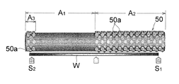
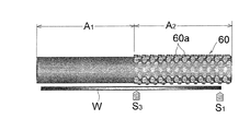
【解決手段】表面に多数のノジュールを有し基板の直径のほぼ全長に亘って直線状に延びて基板表面との間に洗浄エリアを形成するロール洗浄部材と基板とを共に一方向に回転させつつ、ノジュールと基板表面とを互いに接触させて該表面をスクラブ洗浄する基板洗浄方法において、洗浄エリア(長さL)上のロール洗浄部材16と基板Wの相対回転速度が相対的に低い順方向洗浄エリア(長さLf)では、洗浄エリア上のロール洗浄部材と基板の相対回転速度が相対的に高い逆方向洗浄エリア(長さLi)よりも少ない面積でノジュール16aと基板Wの表面とを互いに接触させる。
【選択図】図6
Description
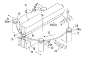
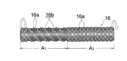
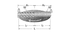
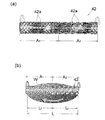
図1は、本発明の基板洗浄方法に使用されるスクラブ洗浄装置の一例を示す概要図である。図1に示すように、このスクラブ洗浄装置は、表面を上にして半導体ウエハ等の基板Wの周縁部を支持し基板Wを水平回転させる、水平方向に移動自在な複数本(図では4本)のスピンドル10と、スピンドル10で支持して回転させる基板Wの上方に昇降自在に配置される上部ロールホルダ12と、スピンドル10で支持して回転させる基板Wの下方に昇降自在に配置される下部ロールホルダ14を備えている。
12 上部ロールホルダ
14 下部ロールホルダ
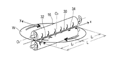
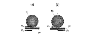
16 上部ロール洗浄部材(ロールスポンジ)
16a ノジュール
16b 螺旋溝
18 下部ロール洗浄部材(ロールスポンジ)
24 コマ
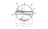
30 洗浄エリア
32 順方向洗浄エリア
34 逆方向洗浄エリア
Lf 順方向洗浄エリアの長さ
Li 逆方向洗浄エリアの長さ
A1 順方向洗浄エリアに対応する領域
A2 逆方向洗浄エリアに対応する領域
Claims (6)
- 表面に多数のノジュールを有し基板の直径のほぼ全長に亘って直線状に延びて基板表面との間に洗浄エリアを形成するロール洗浄部材と基板とを共に一方向に回転させつつ、前記ノジュールと基板表面とを互いに接触させて該表面をスクラブ洗浄する基板洗浄方法において、
前記洗浄エリア上の前記ロール洗浄部材と基板の相対回転速度が相対的に低い順方向洗浄エリアでは、前記洗浄エリア上の前記ロール洗浄部材と基板の相対回転速度が相対的に高い逆方向洗浄エリアよりも少ない面積で前記ノジュールと基板表面とを互いに接触させることを特徴とする基板洗浄方法。 - 前記ロール洗浄部材の回転に伴って、基板上の前記順方向洗浄エリアに存在する洗浄液を基板の中心部から外周部に向かって掻き出すことを特徴とする請求項1記載の基板洗浄方法。
- 表面に多数のノジュールを有し基板の直径のほぼ全長に亘って直線状に延びて基板表面との間に洗浄エリアを形成するロール洗浄部材と基板とを共に一方向に回転させつつ、前記ノジュールと基板表面とを互いに接触させて該表面をスクラブ洗浄する基板洗浄方法において、
前記洗浄エリア上の前記ロール洗浄部材と基板の相対回転速度が相対的に高い逆方向洗浄エリア、及び前記洗浄エリア上の前記ロール洗浄部材と基板の相対回転速度が相対的に低い順方向洗浄エリアの反逆方向洗浄エリア側端部のみで前記ノジュールと基板表面とを互いに接触させることを特徴とする基板洗浄方法。 - 表面に多数のノジュールを有し、基板の直径のほぼ全長に亘って直線状に延びて基板表面との間に洗浄エリアを形成し、基板と共に一方向に回転させつつ前記ノジュールと基板表面とを互いに接触させて該表面をスクラブ洗浄するロール洗浄部材であって、
前記洗浄エリア上の基板との相対回転速度が相対的に低い順方向洗浄エリアに対応する領域に設けられる前記ノジュールの分布密度を、前記洗浄エリア上の基板との相対回転速度が相対的に高い逆方向洗浄エリアに対応する領域に設けられる前記ノジュールの分布密度より低くしたことを特徴とするロール洗浄部材。 - 前記順方向洗浄エリアに対応する領域には、回転に伴って、洗浄液を基板の中心部から外周部に向かって掻き出す方向に螺旋状に連続した螺旋溝がノジュール間に形成されるように、前記ノジュールが設けられていることを特徴とする請求項4記載のロール洗浄部材。
- 表面に多数のノジュールを有し、基板の直径のほぼ全長に亘って直線状に延びて基板表面との間に洗浄エリアを形成し、基板とを共に一方向に回転させつつ前記ノジュールと基板表面とを互いに接触させて該表面をスクラブ洗浄するロール洗浄部材であって、
前記洗浄エリア上の基板との相対回転速度が相対的に高い逆方向洗浄エリアに対応する領域、及び前記洗浄エリア上の基板との相対回転速度が相対的に低い順方向洗浄エリアの反逆方向洗浄エリア側端部に対応する領域のみに前記ノジュールが設けられていることを特徴とするロール洗浄部材。
Priority Applications (4)
| Application Number | Priority Date | Filing Date | Title |
|---|---|---|---|
| JP2011116690A JP5645752B2 (ja) | 2011-05-25 | 2011-05-25 | 基板洗浄方法及びロール洗浄部材 |
| US13/478,373 US9011605B2 (en) | 2011-05-25 | 2012-05-23 | Substrate cleaning method and roll cleaning member |
| KR1020120055161A KR101554767B1 (ko) | 2011-05-25 | 2012-05-24 | 기판 세정 방법 및 롤 세정 부재 |
| TW101118532A TWI512808B (zh) | 2011-05-25 | 2012-05-24 | Substrate cleaning method and roller cleaning components |
Applications Claiming Priority (1)
| Application Number | Priority Date | Filing Date | Title |
|---|---|---|---|
| JP2011116690A JP5645752B2 (ja) | 2011-05-25 | 2011-05-25 | 基板洗浄方法及びロール洗浄部材 |
Publications (2)
| Publication Number | Publication Date |
|---|---|
| JP2012248564A true JP2012248564A (ja) | 2012-12-13 |
| JP5645752B2 JP5645752B2 (ja) | 2014-12-24 |
Family
ID=47292094
Family Applications (1)
| Application Number | Title | Priority Date | Filing Date |
|---|---|---|---|
| JP2011116690A Active JP5645752B2 (ja) | 2011-05-25 | 2011-05-25 | 基板洗浄方法及びロール洗浄部材 |
Country Status (4)
| Country | Link |
|---|---|
| US (1) | US9011605B2 (ja) |
| JP (1) | JP5645752B2 (ja) |
| KR (1) | KR101554767B1 (ja) |
| TW (1) | TWI512808B (ja) |
Cited By (2)
| Publication number | Priority date | Publication date | Assignee | Title |
|---|---|---|---|---|
| KR20150061773A (ko) * | 2013-11-28 | 2015-06-05 | 주식회사 케이씨텍 | 기판 세정 장치 |
| JP2025065128A (ja) * | 2019-09-10 | 2025-04-17 | イリノイ トゥール ワークス インコーポレイティド | 一定でないノジュール密度を有するブラシ |
Families Citing this family (7)
| Publication number | Priority date | Publication date | Assignee | Title |
|---|---|---|---|---|
| TW201235155A (en) * | 2011-02-25 | 2012-09-01 | Hon Hai Prec Ind Co Ltd | Cleaning scrap device for grinding plate |
| TWI636518B (zh) * | 2013-04-23 | 2018-09-21 | 荏原製作所股份有限公司 | 基板處理裝置及處理基板之製造方法 |
| CN107078046B (zh) * | 2014-10-31 | 2020-11-27 | 株式会社荏原制作所 | 基板清洗辊、基板清洗装置及基板清洗方法 |
| KR102573572B1 (ko) * | 2017-12-20 | 2023-09-01 | 삼성전자주식회사 | 웨이퍼 세정 장치 |
| JP7166132B2 (ja) * | 2018-10-12 | 2022-11-07 | 株式会社荏原製作所 | 基板洗浄部材および基板洗浄装置 |
| JP2022134658A (ja) * | 2021-03-03 | 2022-09-15 | アイオン株式会社 | ブラシローラ |
| WO2025111537A1 (en) * | 2023-11-22 | 2025-05-30 | Tech Core Pva, Llc | Cylindrical brush with varying brush nodule length |
Citations (4)
| Publication number | Priority date | Publication date | Assignee | Title |
|---|---|---|---|---|
| JP2001358110A (ja) * | 2000-06-13 | 2001-12-26 | Hitachi Ltd | スクラブ洗浄装置およびそれを用いた半導体装置の製造方法 |
| JP2002280344A (ja) * | 2001-03-16 | 2002-09-27 | Ebara Corp | 基板処理装置 |
| JP2009066527A (ja) * | 2007-09-13 | 2009-04-02 | Nec Electronics Corp | 洗浄用ローラおよび洗浄装置 |
| JP2009117765A (ja) * | 2007-11-09 | 2009-05-28 | Aion Kk | 洗浄用スポンジローラ |
Family Cites Families (10)
| Publication number | Priority date | Publication date | Assignee | Title |
|---|---|---|---|---|
| JPH10308374A (ja) | 1997-03-06 | 1998-11-17 | Ebara Corp | 洗浄方法及び洗浄装置 |
| JP2000015190A (ja) | 1998-07-03 | 2000-01-18 | Matsushita Electric Ind Co Ltd | 基板洗浄方法及び装置 |
| US6299698B1 (en) * | 1998-07-10 | 2001-10-09 | Applied Materials, Inc. | Wafer edge scrubber and method |
| JP2002043267A (ja) | 2000-07-21 | 2002-02-08 | Ebara Corp | 基板洗浄装置、基板洗浄方法及び基板処理装置 |
| JP2002313767A (ja) | 2001-04-17 | 2002-10-25 | Ebara Corp | 基板処理装置 |
| US6616516B1 (en) * | 2001-12-13 | 2003-09-09 | Lam Research Corporation | Method and apparatus for asymmetric processing of front side and back side of semiconductor substrates |
| US6733596B1 (en) * | 2002-12-23 | 2004-05-11 | Lam Research Corporation | Substrate cleaning brush preparation sequence, method, and system |
| US20050109371A1 (en) * | 2003-10-27 | 2005-05-26 | Applied Materials, Inc. | Post CMP scrubbing of substrates |
| JP2008282865A (ja) | 2007-05-08 | 2008-11-20 | Fuji Electric Device Technology Co Ltd | スクラブ洗浄装置及びそれに用いられるロールスポンジアセンブリ |
| TWM362051U (en) * | 2009-02-26 | 2009-08-01 | Tung An Dev Ltd | Structure for cleaning |
-
2011
- 2011-05-25 JP JP2011116690A patent/JP5645752B2/ja active Active
-
2012
- 2012-05-23 US US13/478,373 patent/US9011605B2/en active Active
- 2012-05-24 TW TW101118532A patent/TWI512808B/zh active
- 2012-05-24 KR KR1020120055161A patent/KR101554767B1/ko active Active
Patent Citations (4)
| Publication number | Priority date | Publication date | Assignee | Title |
|---|---|---|---|---|
| JP2001358110A (ja) * | 2000-06-13 | 2001-12-26 | Hitachi Ltd | スクラブ洗浄装置およびそれを用いた半導体装置の製造方法 |
| JP2002280344A (ja) * | 2001-03-16 | 2002-09-27 | Ebara Corp | 基板処理装置 |
| JP2009066527A (ja) * | 2007-09-13 | 2009-04-02 | Nec Electronics Corp | 洗浄用ローラおよび洗浄装置 |
| JP2009117765A (ja) * | 2007-11-09 | 2009-05-28 | Aion Kk | 洗浄用スポンジローラ |
Cited By (3)
| Publication number | Priority date | Publication date | Assignee | Title |
|---|---|---|---|---|
| KR20150061773A (ko) * | 2013-11-28 | 2015-06-05 | 주식회사 케이씨텍 | 기판 세정 장치 |
| KR102063464B1 (ko) | 2013-11-28 | 2020-01-08 | 주식회사 케이씨텍 | 기판 세정 장치 |
| JP2025065128A (ja) * | 2019-09-10 | 2025-04-17 | イリノイ トゥール ワークス インコーポレイティド | 一定でないノジュール密度を有するブラシ |
Also Published As
| Publication number | Publication date |
|---|---|
| KR20120132380A (ko) | 2012-12-05 |
| KR101554767B1 (ko) | 2015-09-21 |
| US9011605B2 (en) | 2015-04-21 |
| TW201301373A (zh) | 2013-01-01 |
| US20120312323A1 (en) | 2012-12-13 |
| TWI512808B (zh) | 2015-12-11 |
| JP5645752B2 (ja) | 2014-12-24 |
Similar Documents
| Publication | Publication Date | Title |
|---|---|---|
| JP5645752B2 (ja) | 基板洗浄方法及びロール洗浄部材 | |
| JP5886224B2 (ja) | 基板洗浄方法 | |
| JP5775383B2 (ja) | 基板洗浄方法 | |
| JP6366544B2 (ja) | 洗浄装置及びロール洗浄部材 | |
| CN107078046B (zh) | 基板清洗辊、基板清洗装置及基板清洗方法 | |
| JP6901277B2 (ja) | スクラブ洗浄方法およびスクラブ洗浄装置 | |
| TWI590319B (zh) | 化學機械研磨後清洗及設備 | |
| KR20160052343A (ko) | 롤 부재, 펜슬 부재 및 그들 중 적어도 어느 한쪽을 포함하는 기판 처리 장치 | |
| JP5661564B2 (ja) | 洗浄性能予測方法及び基板洗浄方法 | |
| KR20230047021A (ko) | 세정 장치 |
Legal Events
| Date | Code | Title | Description |
|---|---|---|---|
| A621 | Written request for application examination |
Free format text: JAPANESE INTERMEDIATE CODE: A621 Effective date: 20130911 |
|
| A977 | Report on retrieval |
Free format text: JAPANESE INTERMEDIATE CODE: A971007 Effective date: 20140709 |
|
| A131 | Notification of reasons for refusal |
Free format text: JAPANESE INTERMEDIATE CODE: A131 Effective date: 20140715 |
|
| A521 | Request for written amendment filed |
Free format text: JAPANESE INTERMEDIATE CODE: A523 Effective date: 20140911 |
|
| TRDD | Decision of grant or rejection written | ||
| A01 | Written decision to grant a patent or to grant a registration (utility model) |
Free format text: JAPANESE INTERMEDIATE CODE: A01 Effective date: 20141014 |
|
| A61 | First payment of annual fees (during grant procedure) |
Free format text: JAPANESE INTERMEDIATE CODE: A61 Effective date: 20141104 |
|
| R150 | Certificate of patent or registration of utility model |
Ref document number: 5645752 Country of ref document: JP Free format text: JAPANESE INTERMEDIATE CODE: R150 |
|
| R250 | Receipt of annual fees |
Free format text: JAPANESE INTERMEDIATE CODE: R250 |
|
| R250 | Receipt of annual fees |
Free format text: JAPANESE INTERMEDIATE CODE: R250 |
|
| R250 | Receipt of annual fees |
Free format text: JAPANESE INTERMEDIATE CODE: R250 |
|
| R250 | Receipt of annual fees |
Free format text: JAPANESE INTERMEDIATE CODE: R250 |
|
| R250 | Receipt of annual fees |
Free format text: JAPANESE INTERMEDIATE CODE: R250 |
|
| R250 | Receipt of annual fees |
Free format text: JAPANESE INTERMEDIATE CODE: R250 |
|
| R250 | Receipt of annual fees |
Free format text: JAPANESE INTERMEDIATE CODE: R250 |
|
| R250 | Receipt of annual fees |
Free format text: JAPANESE INTERMEDIATE CODE: R250 |
|
| R250 | Receipt of annual fees |
Free format text: JAPANESE INTERMEDIATE CODE: R250 |