JP2012058860A - メモリシステム - Google Patents
メモリシステム Download PDFInfo
- Publication number
- JP2012058860A JP2012058860A JP2010199381A JP2010199381A JP2012058860A JP 2012058860 A JP2012058860 A JP 2012058860A JP 2010199381 A JP2010199381 A JP 2010199381A JP 2010199381 A JP2010199381 A JP 2010199381A JP 2012058860 A JP2012058860 A JP 2012058860A
- Authority
- JP
- Japan
- Prior art keywords
- chip
- current
- memory
- sub
- high current
- Prior art date
- Legal status (The legal status is an assumption and is not a legal conclusion. Google has not performed a legal analysis and makes no representation as to the accuracy of the status listed.)
- Pending
Links
Images


Classifications
-
- G—PHYSICS
- G11—INFORMATION STORAGE
- G11C—STATIC STORES
- G11C16/00—Erasable programmable read-only memories
- G11C16/02—Erasable programmable read-only memories electrically programmable
- G11C16/06—Auxiliary circuits, e.g. for writing into memory
- G11C16/10—Programming or data input circuits
-
- G—PHYSICS
- G11—INFORMATION STORAGE
- G11C—STATIC STORES
- G11C16/00—Erasable programmable read-only memories
- G11C16/02—Erasable programmable read-only memories electrically programmable
- G11C16/06—Auxiliary circuits, e.g. for writing into memory
- G11C16/30—Power supply circuits
Abstract
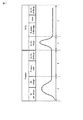
【解決手段】チップ1は、コントローラ20から第1制御信号を受け取ると、第1動作のうちの第1サブ動作を実行して、第1動作を中断する。コントローラ20は第1動作が中断されると、第2制御信号をチップ2に送信する。第2制御信号を受け取ると、チップ2は第2動作のうちの第3サブ動作を実行して、第2動作を中断する。コントローラ20は第2動作が中断されると、第3制御信号をチップ1に送信する。第3制御信号を受け取ると、チップ1は第1動作を再開し、第2サブ動作を実行する。コントローラ20は第2サブ動作が終了すると、第4制御信号をチップ2に送信する。第4制御信号を受け取ると、チップ2は第2動作を再開し、第4サブ動作を実行する。
【選択図】図5
Description
第1実施形態のメモリシステムについて説明する。
次に、第2実施形態のメモリシステムについて説明する。
Claims (6)
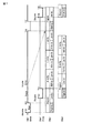
- 複数のメモリセルを有し、前記複数のメモリセルに対して書き込み、読み出し及び消去の少なくともいずれか1つの第1動作を行う第1の不揮発性半導体メモリと、
複数のメモリセルを有し、前記複数のメモリセルに対して書き込み、読み出し及び消去の少なくともいずれか1つの第2動作を行う第2の不揮発性半導体メモリと、
前記第1の不揮発性半導体メモリ及び前記第2の不揮発性半導体メモリの前記第1動作及び前記第2動作を制御するコントローラとを具備し、
前記第1動作は、所定電流以上の電流を消費する第1サブ動作及び第2サブ動作を含み、
前記第2動作は、所定電流以上の電流を消費する第3サブ動作及び第4サブ動作を含み、
前記第1の不揮発性半導体メモリは、前記コントローラから第1制御信号を受け取ると、前記第1動作の前記第1サブ動作を実行した後、前記第1動作を中断し、
前記コントローラは前記第1動作が中断されたことを認知すると、第2制御信号を前記第2の不揮発性半導体メモリに送信し、
前記第2の不揮発性半導体メモリは、前記コントローラから前記第2制御信号を受け取ると、前記第2動作の前記第3サブ動作を実行した後、前記第2動作を中断し、
前記コントローラは前記第2動作が中断されたことを認知すると、第3制御信号を前記第1の不揮発性半導体メモリに送信し、
前記第1の不揮発性半導体メモリは、前記コントローラから前記第3制御信号を受け取ると、前記第1動作を再開して前記第2サブ動作を実行し、
前記コントローラは前記第2サブ動作が実行されたことを認知すると、第4制御信号を前記第2の不揮発性半導体メモリに送信し、
前記第2の不揮発性半導体メモリは、前記コントローラから前記第4制御信号を受け取ると、前記第2動作を再開して前記第4サブ動作を実行することを特徴とするメモリシステム。 - 前記第1サブ動作は前記所定電流以上の電流を消費する第1高電流動作と前記第1高電流動作より小さい電流を消費する第1低電流動作とを含み、前記第2サブ動作は前記所定電流以上の電流を消費する第2高電流動作と前記第2高電流動作より小さい電流を消費する第2低電流動作とを含み、
前記第3サブ動作は前記所定電流以上の電流を消費する第3高電流動作と前記第3高電流動作より小さい電流を消費する第3低電流動作とを含み、前記第4サブ動作は前記所定電流以上の電流を消費する第4高電流動作と前記第4高電流動作より小さい電流を消費する第4低電流動作とを含み、
前記第2高電流動作と前記第1低電流動作とが並行して実行され、前記第3高電流動作と前記第2低電流動作とが並行して実行され、前記第4高電流動作と前記第3低電流動作とが並行して実行されることを特徴とする請求項1に記載のメモリシステム。 - 前記第1動作及び第2動作は書き込みであり、前記第1サブ動作及び前記第3サブ動作はメモリセルにデータを書き込むプログラムであり、前記第2サブ動作及び前記第4サブ動作は前記プログラムが正常に行われたか否かを検証するプログラムベリファイであることを特徴とする請求項1に記載のメモリシステム。
- 前記第1動作及び前記第2動作は読み出しであり、前記第1サブ動作及び前記第3サブ動作は第1ワード線に接続されたメモリセルの読み出しであり、前記第2サブ動作及び前記第4サブ動作は前記第1ワード線に隣接する第2ワード線に接続されたメモリセルの読み出しであることを特徴とする請求項1に記載のメモリシステム。
- 複数のメモリセルを有するメモリセルアレイと、
前記メモリセルアレイに対して書き込み、読み出し及び消去の少なくともいずれか1つの第1動作を行う第1制御回路とを備える第1の不揮発性半導体メモリと、
複数のメモリセルを有するメモリセルアレイと、
前記メモリセルアレイに対して書き込み、読み出し及び消去の少なくともいずれか1つの第2動作を行う第2制御回路とを備える第2の不揮発性半導体メモリと、
前記第1の不揮発性半導体メモリ及び前記第2の不揮発性半導体メモリにそれぞれ設けられ、前記第1の不揮発性半導体メモリ及び前記第2の不揮発性半導体メモリが共にレディ状態であるか否かを検出する検出回路とを具備し、
前記検出回路が前記第1の不揮発性半導体メモリ及び前記第2の不揮発性半導体メモリが共にレディ状態であることを検出したとき、
前記第1制御回路は、第1待機時間の経過後に前記第1動作を開始し、
前記第2制御回路は、前記第1待機時間と異なる第2待機時間の経過後に前記第2動作を開始することを特徴とするメモリシステム。 - 前記第1動作は所定電流以上の電流を消費する第1高電流動作と前記第1高電流動作より小さい電流を消費する第1低電流動作とを含み、
前記第2動作は所定電流以上の電流を消費する第2高電流動作と前記第2高電流動作より小さい電流を消費する第2低電流動作とを含み、
前記第2待機時間は、前記第1動作が含む前記第1高電流動作が終了する時間に設定され、前記第1低電流動作と前記第2高電流動作とが並行して実行されることを特徴とする請求項5に記載のメモリシステム。
Priority Applications (2)
| Application Number | Priority Date | Filing Date | Title |
|---|---|---|---|
| JP2010199381A JP2012058860A (ja) | 2010-09-06 | 2010-09-06 | メモリシステム |
| US13/226,180 US8902662B2 (en) | 2010-09-06 | 2011-09-06 | Memory system having nonvolatile semiconductor memories with control operation having high-current and low-current periods |
Applications Claiming Priority (1)
| Application Number | Priority Date | Filing Date | Title |
|---|---|---|---|
| JP2010199381A JP2012058860A (ja) | 2010-09-06 | 2010-09-06 | メモリシステム |
Publications (2)
| Publication Number | Publication Date |
|---|---|
| JP2012058860A true JP2012058860A (ja) | 2012-03-22 |
| JP2012058860A5 JP2012058860A5 (ja) | 2013-11-07 |
Family
ID=45806608
Family Applications (1)
| Application Number | Title | Priority Date | Filing Date |
|---|---|---|---|
| JP2010199381A Pending JP2012058860A (ja) | 2010-09-06 | 2010-09-06 | メモリシステム |
Country Status (2)
| Country | Link |
|---|---|
| US (1) | US8902662B2 (ja) |
| JP (1) | JP2012058860A (ja) |
Cited By (3)
| Publication number | Priority date | Publication date | Assignee | Title |
|---|---|---|---|---|
| JP2016514323A (ja) * | 2013-03-28 | 2016-05-19 | インテル・コーポレーション | マルチダイnandメモリメモリデバイスのための自動中断動作および自動再開動作 |
| WO2018055734A1 (ja) * | 2016-09-23 | 2018-03-29 | 東芝メモリ株式会社 | メモリデバイス |
| JP7467692B2 (ja) | 2020-11-26 | 2024-04-15 | 長江存儲科技有限責任公司 | マルチダイ動作のための動的なピーク電力管理 |
Families Citing this family (57)
| Publication number | Priority date | Publication date | Assignee | Title |
|---|---|---|---|---|
| US8751755B2 (en) | 2007-12-27 | 2014-06-10 | Sandisk Enterprise Ip Llc | Mass storage controller volatile memory containing metadata related to flash memory storage |
| US9261940B2 (en) * | 2011-02-25 | 2016-02-16 | Samsung Electronics Co., Ltd. | Memory system controlling peak current generation for a plurality of memories by monitoring a peak signal to synchronize an internal clock of each memory by a processor clock at different times |
| JP5713772B2 (ja) * | 2011-04-12 | 2015-05-07 | 株式会社東芝 | 半導体メモリシステム |
| US9699263B1 (en) | 2012-08-17 | 2017-07-04 | Sandisk Technologies Llc. | Automatic read and write acceleration of data accessed by virtual machines |
| US9329986B2 (en) * | 2012-09-10 | 2016-05-03 | Sandisk Technologies Inc. | Peak current management in multi-die non-volatile memory devices |
| US9501398B2 (en) | 2012-12-26 | 2016-11-22 | Sandisk Technologies Llc | Persistent storage device with NVRAM for staging writes |
| US9239751B1 (en) | 2012-12-27 | 2016-01-19 | Sandisk Enterprise Ip Llc | Compressing data from multiple reads for error control management in memory systems |
| US9612948B2 (en) | 2012-12-27 | 2017-04-04 | Sandisk Technologies Llc | Reads and writes between a contiguous data block and noncontiguous sets of logical address blocks in a persistent storage device |
| US9454420B1 (en) | 2012-12-31 | 2016-09-27 | Sandisk Technologies Llc | Method and system of reading threshold voltage equalization |
| US9870830B1 (en) | 2013-03-14 | 2018-01-16 | Sandisk Technologies Llc | Optimal multilevel sensing for reading data from a storage medium |
| US9244763B1 (en) | 2013-03-15 | 2016-01-26 | Sandisk Enterprise Ip Llc | System and method for updating a reading threshold voltage based on symbol transition information |
| US9367246B2 (en) | 2013-03-15 | 2016-06-14 | Sandisk Technologies Inc. | Performance optimization of data transfer for soft information generation |
| US9236886B1 (en) | 2013-03-15 | 2016-01-12 | Sandisk Enterprise Ip Llc | Universal and reconfigurable QC-LDPC encoder |
| US9159437B2 (en) | 2013-06-11 | 2015-10-13 | Sandisk Enterprise IP LLC. | Device and method for resolving an LM flag issue |
| US9524235B1 (en) | 2013-07-25 | 2016-12-20 | Sandisk Technologies Llc | Local hash value generation in non-volatile data storage systems |
| US9384126B1 (en) | 2013-07-25 | 2016-07-05 | Sandisk Technologies Inc. | Methods and systems to avoid false negative results in bloom filters implemented in non-volatile data storage systems |
| US8908463B1 (en) | 2013-07-29 | 2014-12-09 | Kabushiki Kaisha Toshiba | Nonvolatile semiconductor memory device and control method thereof |
| US9639463B1 (en) | 2013-08-26 | 2017-05-02 | Sandisk Technologies Llc | Heuristic aware garbage collection scheme in storage systems |
| US9361221B1 (en) | 2013-08-26 | 2016-06-07 | Sandisk Technologies Inc. | Write amplification reduction through reliable writes during garbage collection |
| US9442662B2 (en) | 2013-10-18 | 2016-09-13 | Sandisk Technologies Llc | Device and method for managing die groups |
| US9298608B2 (en) | 2013-10-18 | 2016-03-29 | Sandisk Enterprise Ip Llc | Biasing for wear leveling in storage systems |
| US9436831B2 (en) | 2013-10-30 | 2016-09-06 | Sandisk Technologies Llc | Secure erase in a memory device |
| US9263156B2 (en) | 2013-11-07 | 2016-02-16 | Sandisk Enterprise Ip Llc | System and method for adjusting trip points within a storage device |
| US9244785B2 (en) | 2013-11-13 | 2016-01-26 | Sandisk Enterprise Ip Llc | Simulated power failure and data hardening |
| US9703816B2 (en) | 2013-11-19 | 2017-07-11 | Sandisk Technologies Llc | Method and system for forward reference logging in a persistent datastore |
| US9520197B2 (en) | 2013-11-22 | 2016-12-13 | Sandisk Technologies Llc | Adaptive erase of a storage device |
| US9520162B2 (en) | 2013-11-27 | 2016-12-13 | Sandisk Technologies Llc | DIMM device controller supervisor |
| US9582058B2 (en) | 2013-11-29 | 2017-02-28 | Sandisk Technologies Llc | Power inrush management of storage devices |
| US9235245B2 (en) | 2013-12-04 | 2016-01-12 | Sandisk Enterprise Ip Llc | Startup performance and power isolation |
| US9361951B2 (en) * | 2014-01-14 | 2016-06-07 | Apple Inc. | Statistical peak-current management in non-volatile memory devices |
| US9703636B2 (en) | 2014-03-01 | 2017-07-11 | Sandisk Technologies Llc | Firmware reversion trigger and control |
| US9390814B2 (en) | 2014-03-19 | 2016-07-12 | Sandisk Technologies Llc | Fault detection and prediction for data storage elements |
| US9454448B2 (en) | 2014-03-19 | 2016-09-27 | Sandisk Technologies Llc | Fault testing in storage devices |
| US9448876B2 (en) | 2014-03-19 | 2016-09-20 | Sandisk Technologies Llc | Fault detection and prediction in storage devices |
| US9390021B2 (en) | 2014-03-31 | 2016-07-12 | Sandisk Technologies Llc | Efficient cache utilization in a tiered data structure |
| US9626399B2 (en) | 2014-03-31 | 2017-04-18 | Sandisk Technologies Llc | Conditional updates for reducing frequency of data modification operations |
| US9626400B2 (en) | 2014-03-31 | 2017-04-18 | Sandisk Technologies Llc | Compaction of information in tiered data structure |
| US9697267B2 (en) | 2014-04-03 | 2017-07-04 | Sandisk Technologies Llc | Methods and systems for performing efficient snapshots in tiered data structures |
| US10656840B2 (en) | 2014-05-30 | 2020-05-19 | Sandisk Technologies Llc | Real-time I/O pattern recognition to enhance performance and endurance of a storage device |
| US9093160B1 (en) * | 2014-05-30 | 2015-07-28 | Sandisk Technologies Inc. | Methods and systems for staggered memory operations |
| US10162748B2 (en) | 2014-05-30 | 2018-12-25 | Sandisk Technologies Llc | Prioritizing garbage collection and block allocation based on I/O history for logical address regions |
| US10656842B2 (en) | 2014-05-30 | 2020-05-19 | Sandisk Technologies Llc | Using history of I/O sizes and I/O sequences to trigger coalesced writes in a non-volatile storage device |
| US10114557B2 (en) | 2014-05-30 | 2018-10-30 | Sandisk Technologies Llc | Identification of hot regions to enhance performance and endurance of a non-volatile storage device |
| US9703491B2 (en) | 2014-05-30 | 2017-07-11 | Sandisk Technologies Llc | Using history of unaligned writes to cache data and avoid read-modify-writes in a non-volatile storage device |
| US10146448B2 (en) | 2014-05-30 | 2018-12-04 | Sandisk Technologies Llc | Using history of I/O sequences to trigger cached read ahead in a non-volatile storage device |
| US10372613B2 (en) | 2014-05-30 | 2019-08-06 | Sandisk Technologies Llc | Using sub-region I/O history to cache repeatedly accessed sub-regions in a non-volatile storage device |
| US9652381B2 (en) | 2014-06-19 | 2017-05-16 | Sandisk Technologies Llc | Sub-block garbage collection |
| US9658789B2 (en) * | 2014-08-05 | 2017-05-23 | Sandisk Technologies Llc | Storage module and method for optimized power utilization |
| US9443601B2 (en) | 2014-09-08 | 2016-09-13 | Sandisk Technologies Llc | Holdup capacitor energy harvesting |
| US10013345B2 (en) * | 2014-09-17 | 2018-07-03 | Sandisk Technologies Llc | Storage module and method for scheduling memory operations for peak-power management and balancing |
| KR102465169B1 (ko) | 2015-12-21 | 2022-11-11 | 에스케이하이닉스 주식회사 | 전자 장치 |
| JP2018156480A (ja) * | 2017-03-17 | 2018-10-04 | 東芝メモリ株式会社 | 半導体記憶装置およびその制御方法 |
| KR102631350B1 (ko) * | 2017-10-12 | 2024-01-31 | 삼성전자주식회사 | 메모리 플레인들을 포함하는 비휘발성 메모리 장치 및 상기 비휘발성 메모리 장치의 동작 방법 |
| US10372373B1 (en) * | 2018-01-29 | 2019-08-06 | Western Digital Technologies, Inc. | Adaptive power balancing for memory device operations |
| JP2019200828A (ja) | 2018-05-16 | 2019-11-21 | 東芝メモリ株式会社 | 半導体記憶装置 |
| JP2021179672A (ja) * | 2020-05-11 | 2021-11-18 | ソニーセミコンダクタソリューションズ株式会社 | メモリモジュール |
| WO2021232233A1 (en) * | 2020-05-19 | 2021-11-25 | Yangtze Memory Technologies Co., Ltd. | Control method and controller of program suspending and resuming for memory |
Citations (1)
| Publication number | Priority date | Publication date | Assignee | Title |
|---|---|---|---|---|
| JP2008197807A (ja) * | 2007-02-09 | 2008-08-28 | Toshiba Corp | 半導体記憶システム |
Family Cites Families (7)
| Publication number | Priority date | Publication date | Assignee | Title |
|---|---|---|---|---|
| JPH11242632A (ja) | 1998-02-26 | 1999-09-07 | Hitachi Ltd | メモリ装置 |
| US6798696B2 (en) * | 2001-12-04 | 2004-09-28 | Renesas Technology Corp. | Method of controlling the operation of non-volatile semiconductor memory chips |
| JP2005267821A (ja) | 2004-03-22 | 2005-09-29 | Toshiba Corp | 不揮発性半導体メモリ |
| JP4955990B2 (ja) * | 2005-12-14 | 2012-06-20 | 株式会社東芝 | 不揮発性半導体記憶装置 |
| JP4928830B2 (ja) | 2006-05-18 | 2012-05-09 | 株式会社東芝 | Nand型フラッシュメモリ装置及びメモリデバイス |
| JP2009151886A (ja) | 2007-12-21 | 2009-07-09 | Toshiba Corp | 半導体記憶装置 |
| US8130550B1 (en) * | 2009-06-24 | 2012-03-06 | Micron Technology, Inc. | Memory with sub-blocks |
-
2010
- 2010-09-06 JP JP2010199381A patent/JP2012058860A/ja active Pending
-
2011
- 2011-09-06 US US13/226,180 patent/US8902662B2/en active Active
Patent Citations (1)
| Publication number | Priority date | Publication date | Assignee | Title |
|---|---|---|---|---|
| JP2008197807A (ja) * | 2007-02-09 | 2008-08-28 | Toshiba Corp | 半導体記憶システム |
Cited By (9)
| Publication number | Priority date | Publication date | Assignee | Title |
|---|---|---|---|---|
| JP2016514323A (ja) * | 2013-03-28 | 2016-05-19 | インテル・コーポレーション | マルチダイnandメモリメモリデバイスのための自動中断動作および自動再開動作 |
| WO2018055734A1 (ja) * | 2016-09-23 | 2018-03-29 | 東芝メモリ株式会社 | メモリデバイス |
| WO2018055814A1 (ja) * | 2016-09-23 | 2018-03-29 | 東芝メモリ株式会社 | メモリデバイス |
| JPWO2018055814A1 (ja) * | 2016-09-23 | 2019-04-25 | 東芝メモリ株式会社 | メモリデバイス |
| JPWO2018055734A1 (ja) * | 2016-09-23 | 2019-06-24 | 東芝メモリ株式会社 | メモリデバイス |
| US10790266B2 (en) | 2016-09-23 | 2020-09-29 | Toshiba Memory Corporation | Memory device with a plurality of stacked memory core chips |
| US10811393B2 (en) | 2016-09-23 | 2020-10-20 | Toshiba Memory Corporation | Memory device |
| US11270981B2 (en) | 2016-09-23 | 2022-03-08 | Kioxia Corporation | Memory device |
| JP7467692B2 (ja) | 2020-11-26 | 2024-04-15 | 長江存儲科技有限責任公司 | マルチダイ動作のための動的なピーク電力管理 |
Also Published As
| Publication number | Publication date |
|---|---|
| US8902662B2 (en) | 2014-12-02 |
| US20120063234A1 (en) | 2012-03-15 |
Similar Documents
| Publication | Publication Date | Title |
|---|---|---|
| JP2012058860A (ja) | メモリシステム | |
| JP4662437B2 (ja) | 半導体集積回路 | |
| JP5905547B1 (ja) | 半導体記憶装置 | |
| JP2010123210A (ja) | 半導体記憶装置 | |
| KR101115623B1 (ko) | 불휘발성 메모리 장치 및 이의 동작 방법 | |
| JP2008040609A (ja) | メモリシステム及びメモリチップ | |
| JP2011040135A (ja) | 不揮発性半導体記憶装置 | |
| US20110113187A1 (en) | Semiconductor device and method for controlling the same | |
| KR20150045644A (ko) | 반도체 장치 및 그 동작 방법 | |
| JP6103664B1 (ja) | 半導体記憶装置 | |
| US8233327B2 (en) | Method of programming nonvolatile memory device | |
| US20100142271A1 (en) | Semiconductor memory device capable of preventing a shift of threshold voltage | |
| JP6983617B2 (ja) | 半導体記憶装置 | |
| US20040228177A1 (en) | Nonvolatile semiconductor memory device and writing method thereto | |
| JP2012128769A (ja) | メモリシステム | |
| US11164645B2 (en) | Semiconductor memory device | |
| JPWO2006090442A1 (ja) | 半導体装置およびその制御方法 | |
| US9019765B2 (en) | Semiconductor device, data programming device, and method for improving the recovery of bit lines of unselected memory cells for programming operation | |
| JP2008052803A (ja) | 不揮発性半導体記憶装置 | |
| US8296499B2 (en) | Flash memory device and program method thereof | |
| JP2008090995A (ja) | フラッシュメモリ装置及びその消去方法 | |
| JP2011023085A (ja) | 半導体記憶装置 | |
| US9520202B1 (en) | Programming verification control circuit and method for control thereof | |
| JP5210812B2 (ja) | 半導体記憶装置及びそのリードアクセス方法 | |
| KR20110078753A (ko) | 반도체 메모리 장치 및 그 동작 방법 |
Legal Events
| Date | Code | Title | Description |
|---|---|---|---|
| A521 | Written amendment |
Free format text: JAPANESE INTERMEDIATE CODE: A523 Effective date: 20130902 |
|
| A621 | Written request for application examination |
Free format text: JAPANESE INTERMEDIATE CODE: A621 Effective date: 20130902 |
|
| A521 | Written amendment |
Free format text: JAPANESE INTERMEDIATE CODE: A523 Effective date: 20130920 |
|
| RD04 | Notification of resignation of power of attorney |
Free format text: JAPANESE INTERMEDIATE CODE: A7424 Effective date: 20131205 |
|
| RD04 | Notification of resignation of power of attorney |
Free format text: JAPANESE INTERMEDIATE CODE: A7424 Effective date: 20131212 |
|
| RD04 | Notification of resignation of power of attorney |
Free format text: JAPANESE INTERMEDIATE CODE: A7424 Effective date: 20131219 |
|
| RD04 | Notification of resignation of power of attorney |
Free format text: JAPANESE INTERMEDIATE CODE: A7424 Effective date: 20131226 |
|
| RD04 | Notification of resignation of power of attorney |
Free format text: JAPANESE INTERMEDIATE CODE: A7424 Effective date: 20140109 |
|
| RD04 | Notification of resignation of power of attorney |
Free format text: JAPANESE INTERMEDIATE CODE: A7424 Effective date: 20140116 |
|
| A977 | Report on retrieval |
Free format text: JAPANESE INTERMEDIATE CODE: A971007 Effective date: 20140213 |
|
| A131 | Notification of reasons for refusal |
Free format text: JAPANESE INTERMEDIATE CODE: A131 Effective date: 20140225 |
|
| A02 | Decision of refusal |
Free format text: JAPANESE INTERMEDIATE CODE: A02 Effective date: 20140708 |