JP2012058860A - Memory system - Google Patents
Memory system Download PDFInfo
- Publication number
- JP2012058860A JP2012058860A JP2010199381A JP2010199381A JP2012058860A JP 2012058860 A JP2012058860 A JP 2012058860A JP 2010199381 A JP2010199381 A JP 2010199381A JP 2010199381 A JP2010199381 A JP 2010199381A JP 2012058860 A JP2012058860 A JP 2012058860A
- Authority
- JP
- Japan
- Prior art keywords
- chip
- current
- memory
- sub
- high current
- Prior art date
- Legal status (The legal status is an assumption and is not a legal conclusion. Google has not performed a legal analysis and makes no representation as to the accuracy of the status listed.)
- Pending
Links
Images


Classifications
-
- G—PHYSICS
- G11—INFORMATION STORAGE
- G11C—STATIC STORES
- G11C16/00—Erasable programmable read-only memories
- G11C16/02—Erasable programmable read-only memories electrically programmable
- G11C16/06—Auxiliary circuits, e.g. for writing into memory
- G11C16/10—Programming or data input circuits
-
- G—PHYSICS
- G11—INFORMATION STORAGE
- G11C—STATIC STORES
- G11C16/00—Erasable programmable read-only memories
- G11C16/02—Erasable programmable read-only memories electrically programmable
- G11C16/06—Auxiliary circuits, e.g. for writing into memory
- G11C16/30—Power supply circuits
Landscapes
- Read Only Memory (AREA)
- Memory System (AREA)
Abstract
Description
本発明の実施形態は、複数の不揮発性半導体メモリを有するメモリシステムに関し、例えば複数のNAND型フラッシュメモリを有するメモリシステムに関するものである。 Embodiments described herein relate generally to a memory system having a plurality of nonvolatile semiconductor memories, for example, a memory system having a plurality of NAND flash memories.
近年、微細化の進行と共に、NAND型フラッシュメモリの書き込みスピードは遅くなっている。一方、複数のNAND型フラッシュメモリチップを有するメモリシステムが扱うデータ量は増加傾向にあるため、メモリシステムは複数のNAND型フラッシュメモリチップに対し同時に書き込みを実行することにより、書き込み性能の向上を図っている。 In recent years, with the progress of miniaturization, the writing speed of the NAND flash memory has been reduced. On the other hand, since the amount of data handled by a memory system having a plurality of NAND flash memory chips tends to increase, the memory system simultaneously improves the writing performance by executing writing to the plurality of NAND flash memory chips. ing.
しかしこの場合、複数のNAND型フラッシュメモリチップを同時に動作させるため、消費電流が増大する。特に、複数のNAND型フラッシュメモリチップにおける消費電流のピークが重なり、大きなピーク電流が流れることが懸念される。 However, in this case, since a plurality of NAND flash memory chips are operated simultaneously, current consumption increases. In particular, there is a concern that a large peak current flows due to overlapping of consumption current peaks in a plurality of NAND flash memory chips.
複数の不揮発性半導体メモリを有するメモリシステムで発生する消費電力のピークを低く抑えることができるメモリシステムを提供する。 Provided is a memory system capable of suppressing a peak of power consumption generated in a memory system having a plurality of nonvolatile semiconductor memories.
一実施態様のメモリシステムは、複数のメモリセルを有し、前記複数のメモリセルに対して書き込み、読み出し及び消去の少なくともいずれか1つの第1動作を行う第1の不揮発性半導体メモリと、複数のメモリセルを有し、前記複数のメモリセルに対して書き込み、読み出し及び消去の少なくともいずれか1つの第2動作を行う第2の不揮発性半導体メモリと、前記第1の不揮発性半導体メモリ及び前記第2の不揮発性半導体メモリの前記第1動作及び前記第2動作を制御するコントローラとを具備する。前記第1動作は、所定電流以上の電流を消費する第1サブ動作及び第2サブ動作を含み、前記第2動作は、所定電流以上の電流を消費する第3サブ動作及び第4サブ動作を含む。前記第1の不揮発性半導体メモリは、前記コントローラから第1制御信号を受け取ると、前記第1動作の前記第1サブ動作を実行した後、前記第1動作を中断し、前記コントローラは前記第1動作が中断されたことを認知すると、第2制御信号を前記第2の不揮発性半導体メモリに送信する。前記第2の不揮発性半導体メモリは、前記コントローラから前記第2制御信号を受け取ると、前記第2動作の前記第3サブ動作を実行した後、前記第2動作を中断し、前記コントローラは前記第2動作が中断されたことを認知すると、第3制御信号を前記第1の不揮発性半導体メモリに送信する。前記第1の不揮発性半導体メモリは、前記コントローラから前記第3制御信号を受け取ると、前記第1動作を再開して前記第2サブ動作を実行し、前記コントローラは前記第2サブ動作が実行されたことを認知すると、第4制御信号を前記第2の不揮発性半導体メモリに送信する。前記第2の不揮発性半導体メモリは、前記コントローラから前記第4制御信号を受け取ると、前記第2動作を再開して前記第4サブ動作を実行することを特徴とする。 A memory system according to an embodiment includes a plurality of memory cells, a first nonvolatile semiconductor memory that performs at least one of write, read, and erase operations on the plurality of memory cells; A second nonvolatile semiconductor memory that performs at least one of writing, reading, and erasing operations on the plurality of memory cells, the first nonvolatile semiconductor memory, A controller for controlling the first operation and the second operation of the second nonvolatile semiconductor memory. The first operation includes a first sub-operation and a second sub-operation that consume a current greater than or equal to a predetermined current, and the second operation includes a third sub-operation and a fourth sub-operation that consumes a current greater than or equal to a predetermined current. Including. When the first nonvolatile semiconductor memory receives the first control signal from the controller, the first nonvolatile semiconductor memory suspends the first operation after executing the first sub-operation of the first operation, and the controller When recognizing that the operation is interrupted, a second control signal is transmitted to the second nonvolatile semiconductor memory. When the second nonvolatile semiconductor memory receives the second control signal from the controller, the second nonvolatile semiconductor memory interrupts the second operation after executing the third sub-operation of the second operation, and the controller When recognizing that the two operations are interrupted, a third control signal is transmitted to the first nonvolatile semiconductor memory. When the first nonvolatile semiconductor memory receives the third control signal from the controller, the first nonvolatile semiconductor memory resumes the first operation and executes the second sub-operation, and the controller executes the second sub-operation. When this is recognized, a fourth control signal is transmitted to the second nonvolatile semiconductor memory. When the second nonvolatile semiconductor memory receives the fourth control signal from the controller, the second nonvolatile semiconductor memory resumes the second operation and executes the fourth sub-operation.
実施形態を説明する前に、本出願を提案するに至った経緯について説明する。 Before describing the embodiment, the background to the proposal of the present application will be described.
複数の不揮発性半導体メモリチップを同時に動作させる場合、消費電流が増大する可能性がある。例えば、複数のNAND型フラッシュメモリチップ(以下、メモリチップ)に対し、同時に書き込みを実行すると、各メモリチップにおいて消費されるピーク電流が重なり、大きな消費電力のピークが発生することが懸念される。なお、以降の説明において、書き込みはプログラムとプログラムベリファイを含むものとする。 When a plurality of nonvolatile semiconductor memory chips are operated at the same time, current consumption may increase. For example, when writing is simultaneously performed on a plurality of NAND flash memory chips (hereinafter referred to as memory chips), there is a concern that peak currents consumed in each memory chip overlap and a large power consumption peak occurs. In the following description, writing includes program and program verify.
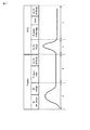
図1に、プログラム(図中「program」と表記、以下同様)とプログラムベリファイ(「Verify」)時のタイミングとその際の消費電流を模式的に示す。プログラムもプログラムベリファイも大きく、ワード線/ビット線のセットアップ(A、C)→書き込みもしくはリード・センス動作→ワード線/ビット線電位のディスチャージ(リカバリ動作)(B、D)といった個々の動作に大別される。なお、図1中、Aは「BL pre-charge」ビット線プリチャージ及び「WL charge」ワード線チャージの意、Bは「program pulse」プログラムパルス及び「WL/BL discharge」ワード線/ビット線ディスチャージの意、Cは「WL/BL charge」ワード線/ビット線チャージの意、Dは「BL isolate & discharge」ビット線のセル電流による放電、「sense」リード・センス動作及び「WL/BL discharge」ワード/ビット線ディスチャージの意を示す。 FIG. 1 schematically shows the timing and current consumption at the time of program (indicated as “program” in the figure, the same applies hereinafter) and program verify (“Verify”). Program and program verify are large, and it is large for individual operations such as word line / bit line setup (A, C) → write or read / sense operation → word line / bit line potential discharge (recovery operation) (B, D) Separated. In FIG. 1, “A” means “BL pre-charge” bit line precharge and “WL charge” word line charge, and “B” means “program pulse” program pulse and “WL / BL discharge” word line / bit line discharge. , C means “WL / BL charge” word line / bit line charge, D means “BL isolate & discharge” discharge due to bit line cell current, “sense” read sense operation and “WL / BL discharge” Indicates the word / bit line discharge.
個々の動作の所要時間は、メモリチップ内部であらかじめ決められたタイマで決まる。メモリチップの消費電流は一定ではなく、ある特定の動作で大きなピーク電流が発生する。 The time required for each operation is determined by a predetermined timer in the memory chip. The current consumption of the memory chip is not constant, and a large peak current is generated in a specific operation.
複数のメモリチップで同時に書き込みを実行したときにも、このピーク電流がメモリチップ間で重ならないようにできればよい。例えば、書き込み実行のタイミングをずらすといった方法が考えられるが、実際にはそれだけでは重なりを防ぐのは困難である。以下に、その例を示す。 Even when writing is performed simultaneously on a plurality of memory chips, it is only necessary to prevent this peak current from overlapping between memory chips. For example, a method of shifting the timing of execution of writing can be considered, but in practice it is difficult to prevent overlap by itself. An example is shown below.
図2に、多値NAND型フラッシュメモリにおけるプログラム(「program」)とプログラムベリファイ(「Verify」)のフローを示す。 FIG. 2 shows a flow of program (“program”) and program verify (“Verify”) in the multi-level NAND flash memory.
多値のNAND型フラッシュメモリでは、しきい値電圧のレベルごとにベリファイを行っているが、レベルごとにプログラムが完了すると、以降該当レベルのベリファイは実施する必要はない。ここでは、3つのレベル(A<B<C)のベリファイを行っている。 In the multi-level NAND flash memory, verification is performed for each level of the threshold voltage. However, when programming is completed for each level, it is not necessary to perform verification of the corresponding level thereafter. Here, verification at three levels (A <B <C) is performed.
また、一般にNAND型フラッシュメモリのメモリセルはしきい値電圧の低いレベルから書き上げて行くので、書き込み開始直後はB,Cレベルのベリファイをある回数実行しないことも、書き込み性能改善のために行われている。 In general, since the memory cell of the NAND flash memory is written from a low threshold voltage level, the B and C level verification is not executed a certain number of times immediately after the start of writing in order to improve the writing performance. ing.
つまり、メモリチップごとにピーク電流が流れるタイミングは異なり、しかもそのタイミングはメモリセルのセル特性に起因する。このため、ピーク電流が流れるタイミングを制御することは困難である。 That is, the timing at which the peak current flows is different for each memory chip, and the timing is due to the cell characteristics of the memory cell. For this reason, it is difficult to control the timing at which the peak current flows.
他の要因として、NAND型フラッシュメモリは、コマンド入力を受けてメモリチップ内に備えたオシレータで、例えば100ns周期のクロックを生成している。このクロックに同期して制御回路(ステートマシン)が動作する。 As another factor, the NAND flash memory is an oscillator provided in the memory chip in response to a command input, and generates a clock of, for example, a cycle of 100 ns. A control circuit (state machine) operates in synchronization with this clock.
タイマ設定が複数のメモリチップで同じ場合でも、このクロック周期にはばらつきが生じる。NAND型フラッシュメモリの書き込みや読み出し時間は数十μs〜数msであるため、クロック周期のばらつきは決して無視できず、どこかでメモリチップ間のピーク電流が重なる可能性がある。 Even when the timer setting is the same for a plurality of memory chips, the clock cycle varies. Since the writing and reading time of the NAND flash memory is several tens of μs to several ms, the variation in the clock cycle can never be ignored, and the peak currents between the memory chips may overlap somewhere.
このように、複数のNAND型フラッシュメモリで同時に書き込みシーケンスが実行されている場合に、それぞれのNAND型フラッシュメモリで発生するピーク電流が重なり、メモリシステムとして非常に大きな消費電流となる懸念があった。このため、メモリシステムはこの最大のピーク電流に対応する電源システムを組み込む必要があった。 As described above, when a write sequence is executed simultaneously in a plurality of NAND flash memories, there is a concern that peak currents generated in the respective NAND flash memories overlap, resulting in a very large current consumption as a memory system. . For this reason, the memory system needs to incorporate a power supply system corresponding to the maximum peak current.
そこで、本実施形態では、複数の不揮発性半導体メモリを有するメモリシステムで発生する消費電力のピークを低く抑えることができるメモリシステムを提供する。 Therefore, the present embodiment provides a memory system that can suppress the peak of power consumption generated in a memory system having a plurality of nonvolatile semiconductor memories.
以下に、図面を参照して実施形態について説明する。なお、以下の説明において、同一の機能及び構成を有する要素については、同一符号を付し、重複説明は必要な場合にのみ行う。 Embodiments will be described below with reference to the drawings. In the following description, elements having the same function and configuration are denoted by the same reference numerals, and redundant description will be given only when necessary.
[1] 第1実施形態
第1実施形態のメモリシステムについて説明する。
[1] First Embodiment A memory system according to a first embodiment will be described.
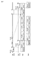
図3は、第1実施形態のメモリシステムの構成を示すブロック図である。 FIG. 3 is a block diagram illustrating a configuration of the memory system according to the first embodiment.
図示するように、メモリシステム10は、複数の不揮発性半導体メモリチップ、例えばNAND型フラッシュメモリチップ(以下、メモリチップ)10−1,10−2,10−3,10−4、コントローラ20を備える。コントローラ20は、メモリチップ10−1,10−2,10−3,10−4の動作を制御する。
As illustrated, the
メモリチップの各々は、メモリセルアレイ11、主制御部12、ブロック制御回路13、ロウ制御回路14、選択回路15、センスアンプ16、カラム制御回路17、データ入出力バッファ18、入出力制御回路19を備える。
Each of the memory chips includes a
主制御部12は、コントローラ20から出力された制御信号を入出力制御回路19及びデータ入出力バッファ18を介して受け取り、制御信号に基づいてブロック制御回路13、ロウ制御回路14、選択回路15、センスアンプ16及びカラム制御回路17を制御して、メモリセルアレイ11に対するデータの書き込み、読み出し及び消去を行う。
The
ブロック制御回路13は、メモリセルアレイ11に含まれるブロックの選択を制御する。ロウ制御回路14は、メモリセルアレイ11に対するデータの書き込み、読み出し及び消去時にメモリセルアレイ11内のワード線に対して印加する電圧の制御を行う。
The
カラム制御回路17は、カラムアドレスに基づいてメモリセルアレイ11内のビット線の選択を制御する。センスアンプ16は、選択されたビット線に接続されたメモリセルから選択回路15を介してデータを読み出す。
The column control circuit 17 controls selection of the bit line in the
メモリセルアレイ11は複数のブロックを備え、ブロックの各々は複数のNAND列を有する。NAND列の各々は直列に接続された複数のメモリセルを有し、メモリセルの各々は、浮遊ゲートと、浮遊ゲート上にゲート間絶縁膜を介して配置された制御ゲートとを持つ不揮発性のメモリセルトランジスタからなる。
The
次に、第1実施形態のメモリシステムにおける書き込み時の動作を説明する。ここでは、2個のNAND型フラッシュメモリチップ10−1,10−2における書き込み動作を述べるが、メモリチップが3個以上の場合も同様の手法で書き込み動作を行うことができる。 Next, the operation at the time of writing in the memory system of the first embodiment will be described. Here, the write operation in the two NAND flash memory chips 10-1 and 10-2 will be described, but the write operation can be performed by the same method even when there are three or more memory chips.
図4は、第1実施形態のNAND型フラッシュメモリチップ10−1,10−2における書き込み時のフローチャートである。図5は、第1実施形態における書き込み時のタイミングチャートである。 FIG. 4 is a flowchart at the time of writing in the NAND flash memory chips 10-1 and 10-2 of the first embodiment. FIG. 5 is a timing chart at the time of writing in the first embodiment.
まず、メモリチップ10−1,10−2内の主制御部12は、コントローラ20からレジュームコマンドが入力されるまで待機する((「Wait Resume Command」)ステップS1)。主制御部12は、コントローラ20からレジュームコマンドを受け取ると、プログラムをスタートさせ((「Program start」)ステップS2)、プログラムを実行する((「Program」)ステップS3)。プログラムは、図5に示すように、ビット線のプリチャージ、ワード線のチャージ、プログラムパルスの印加、及びワード線/ビット線電位のディスチャージといった順序で行われる。
First, the
プログラムが終了すると((「program end」)ステップS4)、主制御部12はメモリチップをサスペンド状態(一時中断状態)とし、再び、コントローラ20からレジュームコマンドが入力されるまで待機する((「Wait Resume Command」)ステップS5)。
When the program ends ((“program end”) step S4), the
次に、主制御部12は、レジュームコマンドを受け取ると、プログラムベリファイをスタートさせ((「Verify start」)ステップS6)、プログラムベリファイを実行する((「Verify」)ステップS7)。プログラムベリファイは、図5に示すように、ワード線/ビット線のチャージ、ビット線のセル電流による放電、リード・センス動作、及びワード線/ビット線電位のディスチャージといった順序で行われる。
Next, when receiving the resume command, the
プログラムベリファイが終了すると((「Verify end」)ステップS8)、主制御部12はメモリセルに対してベリファイがパスしたか否かを判定する((「Verify Pass」)ステップS9)。ベリファイをパスしているとき、書き込み動作を終了する((「End」)ステップS10)。
When the program verification is completed ((“Verify end”) step S8), the
一方、ベリファイをパスしていないとき、主制御部12はメモリチップをサスペンド状態とし、再び、コントローラ20からレジュームコマンドが入力されるまで待機する((「Wait Resume Command」)ステップS11)。そして、主制御部12は、コントローラ20からレジュームコマンドを受け取ると、ステップS2に戻り、ステップS2以降の処理を繰り返す。
On the other hand, when the verification is not passed, the
図5を用いて、書き込み時の動作を述べる。なお、図5以降の図では、NAND型フラッシュメモリチップ10−1をチップ1とし、NAND型フラッシュメモリチップ10−2をチップ2とする。チップステータスは、“H”がレディ状態、“L”がビジー状態であることを表す。このレディまたはビジーの出力はメモリチップに出力ピンを設けてもよいし、メモリチップからステータスコマンドを出力してもよい。
The operation at the time of writing will be described with reference to FIG. 5 and the subsequent drawings, the NAND flash memory chip 10-1 is referred to as
まず、コントローラ20は、チップ1がレディ状態であるとき、レジュームコマンド(「Resume」)をチップ1に出力する。チップ1は、レジュームコマンドを受け取ると、プログラム(「program」)をスタートさせる。そして、チップ1は、ビット線のプリチャージ(「BL pre-charge」)を行い、続いてワード線のチャージ(「WL charge」)を行う。ワード線のチャージが終了すると、すなわち高い電流を必要とする期間が終了すると、チップ1はレディ状態であることをコントローラ20に通知する。
First, the
チップ1は、ワード線のチャージが終了した後、続いてプログラムパルスの印加(「program pulse」)、及びワード線/ビット線電位のディスチャージ(「WL/BL discharge」)を行い、プログラムを終了する。プログラムを終了した後、チップ1はサスペンド状態となる。プログラムのうち、ビット線のプリチャージとワード線のチャージを行う期間が高い電流を必要とする期間(高電流期間)であり、プログラムパルスの印加とワード線/ビット線電位のディスチャージを行う期間が低い電流を必要とする期間(低電流期間)である。
After the word line charge is completed, the
コントローラ20は、チップ1がレディ状態であることを認知すると、レジュームコマンドをチップ2に出力する。チップ2は、レジュームコマンドを受け取ると、プログラムをスタートさせる。そして、チップ2は、ビット線のプリチャージを行い、続いてワード線のチャージを行う。このとき、チップ2のこれら高電流期間の動作と並行して、チップ1では、前述したように、低電流期間の動作、すなわちプログラムパルスの印加、及びワード線/ビット線のディスチャージが行われる。ワード線のチャージが終了すると、すなわち高電流期間が終了すると、チップ2はレディ状態であることをコントローラ20に通知する。
When the
チップ2は、ワード線のチャージが終了した後、続いてプログラムパルスの印加、及びワード線/ビット線電位のディスチャージを行い、プログラムを終了する。プログラムを終了した後、チップ2はサスペンド状態となる。
After the charging of the word line is completed, the
コントローラ20は、チップ2がレディ状態であることを認知すると、レジュームコマンドをチップ1に出力する。チップ1は、レジュームコマンドを受け取ると、プログラムベリファイ(「Verify」)をスタートさせる。そして、チップ1は、ワード線/ビット線のチャージ(「WL/BL charge」)を行う。このとき、チップ1のこの高電流期間の動作と並行して、チップ2では、前述したように、低電流期間の動作、すなわちプログラムパルスの印加、及びワード線/ビット線のディスチャージが行われる。チップ1のワード線/ビット線のチャージが終了すると、すなわち高い電流を必要とする期間が終了すると、チップ1はレディ状態であることをコントローラ20に通知する。
When the
チップ1は、ワード線/ビット線のチャージが終了した後、続いてビット線のセル電流による放電(「BL isolate & discharge」)、リード・センス動作(「sense」)、及びワード線/ビット線電位のディスチャージ(「WL/BL discharge」)を行い、プログラムベリファイを終了する。プログラムベリファイを終了した後、チップ1はサスペンド状態となる。プログラムベリファイのうち、ワード線/ビット線のチャージを行う期間が高い電流を必要とする期間(高電流期間)であり、ビット線のセル電流による放電、リード・センス動作、及びワード線/ビット線電位のディスチャージを行う期間が低い電流を必要とする期間(低電流期間)である。
In the
コントローラ20は、チップ1がレディ状態であることを認知すると、レジュームコマンドをチップ2に出力する。チップ2は、レジュームコマンドを受け取ると、プログラムベリファイをスタートさせる。そして、チップ2は、ワード線/ビット線のチャージを行う。このとき、チップ2のこの高電流期間の動作と並行して、チップ1では低電流期間の動作、すなわちビット線のセル電流による放電、リード・センス動作、及びワード線/ビット線電位のディスチャージが行われる。チップ2のワード線/ビット線のチャージが終了すると、チップ2はレディ状態であることをコントローラ20に通知する。
When the
チップ2は、ワード線/ビット線のチャージが終了した後、続いてビット線のセル電流による放電、リード・センス動作、及びワード線/ビット線電位のディスチャージを行い、プログラムベリファイを終了する。プログラムベリファイを終了した後、チップ2はサスペンド状態となる。
After the charge of the word line / bit line is completed, the
このように、NAND型フラッシュメモリチップは、ピーク電流が発生する動作中はビジー状態となり、ビジー状態を示す信号をコントローラ20に出力する。そして、次のピーク電流が発生する動作の前に、サスペンド状態に移行してレジュームコマンドの入力を待つ。
As described above, the NAND flash memory chip is in a busy state during an operation in which a peak current is generated, and outputs a signal indicating the busy state to the
コントローラ20は、メモリチップごとにピーク電流が発生する動作をレディ/ビジーとして把握し、複数のメモリチップ間でビジーが重ならないようにレジュームコマンドを発行することにより、複数のメモリチップ間でピーク電流が発生する動作が重なるのを回避する。すなわち、コントローラ20は、レジュームコマンドの発行タイミングを制御することにより、各々のメモリチップで発生するピーク電流をずらすことができる。これにより、複数のメモリチップを有するメモリシステムにおいて発生する消費電力のピークを低減することが可能である。
The
次に、第1実施形態のメモリシステムにおける書き込み時の動作を3つの例を挙げて詳細に説明する。 Next, the operation at the time of writing in the memory system of the first embodiment will be described in detail with three examples.
図6は、第1実施形態のNAND型フラッシュメモリチップ10−1,10−2における書き込み時のタイミングチャートを示す第1例である。 FIG. 6 is a first example showing a timing chart at the time of writing in the NAND flash memory chips 10-1 and 10-2 of the first embodiment.
この第1例は、プログラムとプログラムベリファイの動作を分離し、レジュームコマンドの入力に応答して、プログラムとプログラムベリファイがそれぞれ動作をスタートするようにしたものである。なお、ピーク電流が流れる高電流期間を“High Icc”、ピーク電流が流れない低電流期間を“Low Icc”で示している。 In this first example, the program and program verify operations are separated, and the program and program verify start operations in response to the input of the resume command. The high current period in which the peak current flows is indicated by “High Icc”, and the low current period in which the peak current does not flow is indicated by “Low Icc”.
チップ1,2において、プログラムの高電流期間、プログラムベリファイの高電流期間がそれぞれ重ならないようにする。プログラムベリファイは、しきい値電圧のレベルごとにベリファイを行っており、ここでは3つのレベル(A<B<C)のベリファイを行うものとする。なお、チップ1におけるプログラムベリファイの高電流期間は、先頭のAベリファイの高電流期間のみとする。また、チップ2では、Aベリファイは以前に既にパスしているものとし、チップ2におけるプログラムベリファイの高電流期間は、先頭のBベリファイの高電流期間のみとする。
In the
以下に、図6に示す書き込み時の動作を詳述する。 The operation at the time of writing shown in FIG. 6 will be described in detail below.
まず、コントローラ20は、チップ1がレディ状態であるとき、レジュームコマンド(「Resume」)をチップ1に出力する(T1)。チップ1は、レジュームコマンドを受け取ると、プログラム(「Program」)をスタートさせる。そして、チップ1は、ピーク電流が流れる高電流期間(High Icc)の動作を行う。高電流期間が終了すると、すなわち高い電流を消費する動作が終了すると、チップ1はレディ状態であることをコントローラ20に通知する(T2)。
First, when the
チップ1は、高電流期間が終了した後、続いてピーク電流が流れない低電流期間(Low Icc)の動作を行い、プログラムを終了する。プログラムを終了した後、チップ1はサスペンド状態となる。前述したように、プログラムのうち、ビット線のプリチャージとワード線のチャージを行う期間が高電流期間であり、プログラムパルスの印加とワード線/ビット線電位のディスチャージを行う期間が低電流期間である。
After the high current period ends, the
コントローラ20は、チップ1がレディ状態であることを認知すると、レジュームコマンドをチップ2に出力する(T3)。チップ2は、レジュームコマンドを受け取ると、プログラムをスタートさせる。そして、チップ2は、高電流期間の動作を行う。このとき、チップ2の高電流期間の動作と並行して、チップ1では低電流期間の動作が行われる。チップ2の高電流期間が終了すると、チップ2はレディ状態であることをコントローラ20に通知する(T4)。
When the
チップ2は、高電流期間が終了した後、続いて低電流期間の動作を行い、プログラムを終了する。プログラムを終了した後、チップ2はサスペンド状態となる。
After the high current period ends, the
コントローラ20は、チップ2がレディ状態であることを認知すると、レジュームコマンドをチップ1に出力する(T5)。チップ1は、レジュームコマンドを受け取ると、プログラムベリファイをスタートさせる。そして、チップ1は、Aベリファイ(「A Verify」)の高電流期間の動作を行う。高電流期間が終了すると、チップ1はレディ状態であることをコントローラ20に通知する(T6)。
When the
チップ1は、高電流期間が終了した後、続いて低電流期間の動作を行う、すなわちAベリファイの低電流期間の動作を行い、さらにBベリファイ(「B Verify」)、Cベリファイ(「C Verify」)を行う。そして、プログラムベリファイを終了する。前述したように、プログラムベリファイのうち、ワード線/ビット線のチャージを行う期間が高い電流を必要とする高電流期間であり、ビット線のセル電流による放電、リード・センス動作、及びワード線/ビット線電位のディスチャージを行う期間が低い電流を必要とする低電流期間である。
After the high current period ends, the
コントローラ20は、チップ1がレディ状態であることを認知すると、レジュームコマンドをチップ2に出力する(T7)。チップ2は、レジュームコマンドを受け取ると、プログラムベリファイをスタートさせる。そして、チップ2は、Bベリファイの高電流期間の動作を行う。このとき、チップ2のこの高電流期間の動作と並行して、チップ1では低電流期間の動作が行われる。チップ2の高電流期間が終了すると、チップ2はレディ状態であることをコントローラ20に通知する(T8)。
When the
チップ2は、高電流期間が終了した後、続いて低電流期間の動作を行う、すなわちBベリファイの低電流期間の動作を行い、さらにCベリファイを行う。そして、プログラムベリファイを終了する。プログラムベリファイを終了した後、チップ2はサスペンド状態となる。
After the end of the high current period, the
コントローラ20は、チップ2がレディ状態であることを認知すると、レジュームコマンドをチップ1に出力する(T9)。チップ1は、レジュームコマンドを受け取り、かつCベリファイが終了したとき、次のプログラムをスタートさせる(T10)。そして、チップ1は、高電流期間の動作を行う。高電流期間が終了すると、チップ1はレディ状態であることをコントローラ20に通知する(T11)。
When the
チップ1は、高電流期間が終了した後、続いて低電流期間の動作を行い、プログラムを終了する。プログラムを終了した後、チップ1はサスペンド状態となる。
After the high current period ends, the
コントローラ20は、チップ1がレディ状態であることを認知すると、レジュームコマンドをチップ2に出力する(T12)。チップ2は、レジュームコマンドを受け取ると、プログラムをスタートさせる。そして、チップ2は、高電流期間の動作を行う。高電流期間が終了すると、チップ2はレディ状態であることをコントローラ20に通知する(T13)。
When the
チップ2は、高電流期間が終了した後、続いて低電流期間の動作を行い、プログラムを終了する。プログラムを終了した後、チップ2はサスペンド状態となる。
After the high current period ends, the
以上のような動作が繰り返される。 The above operation is repeated.
図7は、第1実施形態のNAND型フラッシュメモリチップ10−1,10−2における書き込み時のタイミングチャートを示す第2例である。 FIG. 7 is a second example showing a timing chart at the time of writing in the NAND flash memory chips 10-1 and 10-2 of the first embodiment.
第1例では、プログラムとプログラムベリファイの動作を分離し、レジュームコマンドの入力によってプログラムとプログラムベリファイの動作をそれぞれスタートさせた。この第2例では、プログラムとプログラムベリファイを連続して行われる1つのシーケンスとし、レジュームコマンドの入力に応答して、プログラムとプログラムベリファイの動作が連続して実行される。 In the first example, the program and program verify operations are separated, and the program and program verify operations are started by inputting a resume command. In this second example, the program and program verify are performed as one sequence which is continuously performed, and the program and program verify operations are continuously performed in response to the input of the resume command.
チップ1,2において、プログラムの高電流期間(High Icc)のみが重ならないようにする。すなわち、プログラムの先頭のピーク電流が流れる動作が、チップ1とチップ2とで重ならないようにする。プログラムベリファイは、しきい値電圧のレベルごとにベリファイを行っており、ここでは3つのレベル(A<B<C)のベリファイを行うものとする。なお、チップ1,2におけるプログラムベリファイの高電流期間(High Icc)は、プログラムの高電流期間(High Icc)に比べてピーク電流が少ないものとする。このため、プログラムベリファイの高電流期間は、完全にずれなくてもよい。また、チップ2では、Aベリファイは以前に既にパスしているものとする。
In the
以下に、図7に示す書き込み時の動作を詳述する。 The operation at the time of writing shown in FIG. 7 will be described in detail below.
まず、コントローラ20は、チップ1がレディ状態であるとき、レジュームコマンド(「Resume」)をチップ1に出力する(T21)。チップ1は、レジュームコマンドを受け取ると、プログラム(「Program」)をスタートさせる。そして、チップ1は、ピーク電流が流れる高電流期間(High Icc)の動作を行う。高電流期間が終了すると、すなわち高い電流を消費する動作が終了すると、チップ1はレディ状態であることをコントローラ20に通知する(T22)。
First, when the
チップ1は、高電流期間が終了した後、続いてピーク電流が流れない低電流期間(Low Icc)の動作を行い、プログラムを終了する。さらに、プログラムを終了した後、プログラムベリファイをスタートさせる。そして、チップ1は、Aベリファイ(「A Verify」)、Bベリファイ(「B Verify」)、Cベリファイ(「C Verify」)を行う。
After the high current period ends, the
コントローラ20は、チップ1がレディ状態であることを認知すると、レジュームコマンドをチップ2に出力する(T23)。チップ2は、レジュームコマンドを受け取ると、プログラムをスタートさせる。そして、チップ2は、高電流期間の動作を行う。このとき、チップ2の高電流期間の動作と並行して、チップ1では、前述したように、低電流期間の動作が行われる。チップ2の高電流期間が終了すると、チップ2はレディ状態であることをコントローラ20に通知する(T24)。
When the
チップ2は、高電流期間が終了した後、続いて低電流期間の動作を行い、プログラムを終了する。さらに、プログラムを終了した後、プログラムベリファイをスタートさせる。そして、チップ1は、Bベリファイ、Cベリファイを行う。プログラムベリファイを終了した後、チップ2はサスペンド状態となる。
After the high current period ends, the
コントローラ20は、チップ2がレディ状態であることを認知すると、レジュームコマンドをチップ1に出力する(T25)。チップ1は、レジュームコマンドを受け取り、かつCベリファイが終了したとき、次のプログラムをスタートさせる(T26)。そして、チップ1は、高電流期間の動作を行う。高電流期間が終了すると、チップ1はレディ状態であることをコントローラ20に通知する(T27)。
When the
チップ1は、高電流期間が終了した後、続いて低電流期間の動作を行い、プログラムを終了する。さらに、プログラムを終了した後、プログラムベリファイをスタートさせる。
After the high current period ends, the
コントローラ20は、チップ1がレディ状態であることを認知すると、レジュームコマンドをチップ2に出力する(T28)。チップ2は、レジュームコマンドを受け取ると、プログラムをスタートさせる。そして、チップ2は、高電流期間の動作を行う。高電流期間が終了すると、チップ2はレディ状態であることをコントローラ20に通知する(T29)。
When the
チップ2は、高電流期間が終了した後、続いて低電流期間の動作を行い、プログラムを終了する。さらに、プログラムを終了した後、プログラムベリファイをスタートさせる。
After the high current period ends, the
以上のような動作が繰り返される。 The above operation is repeated.
図8は、第1実施形態のNAND型フラッシュメモリチップ10−1,10−2における書き込み時のタイミングチャートを示す第3例である。 FIG. 8 is a third example showing a timing chart at the time of writing in the NAND flash memory chips 10-1 and 10-2 of the first embodiment.
この第3例では、プログラム、プログラムベリファイにおけるAベリファイ、Bベリファイ、Cベリファイの動作をそれぞれ分離し、レジュームコマンドの入力に応答して、プログラム、Aベリファイ、Bベリファイ、Cベリファイの動作をそれぞれスタートさせる。 In the third example, the operations of A verify, B verify, and C verify in the program and program verify are separated, and the operations of program, A verify, B verify, and C verify are started in response to the input of the resume command. Let
チップ1,2において、プログラムの高電流期間、プログラムベリファイの高電流期間がそれぞれ重ならないようにする。プログラムベリファイは、しきい値電圧のレベルごとにベリファイを行っており、ここでは3つのレベル(A<B<C)のベリファイを行う。なお、チップ1におけるプログラムベリファイの高電流期間は、Aベリファイ、Bベリファイ、Cベリファイにそれぞれ存在するものとする。また、チップ2では、Aベリファイは以前に既にパスしており、チップ2におけるプログラムベリファイの高電流期間は、Bベリファイ、Cベリファイにそれぞれ存在するものとする。
In the
以下に、図8に示す書き込み時の動作を詳述する。 The operation at the time of writing shown in FIG. 8 will be described in detail below.
まず、コントローラ20は、チップ1がレディ状態であるとき、レジュームコマンド(「Resume」)をチップ1に出力する(T31)。チップ1は、レジュームコマンドを受け取ると、プログラム(「Program」)をスタートさせる。そして、チップ1は、ピーク電流が流れる高電流期間(High Icc)の動作を行う。高電流期間が終了すると、すなわち高い電流を消費する動作が終了すると、チップ1はレディ状態であることをコントローラ20に通知する(T32)。
First, when the
チップ1は、高電流期間が終了した後、続いてピーク電流が流れない低電流期間(Low Icc)の動作を行い、プログラムを終了する。プログラムを終了した後、チップ1はサスペンド状態となる。
After the high current period ends, the
コントローラ20は、チップ1がレディ状態であることを認知すると、レジュームコマンドをチップ2に出力する(T33)。チップ2は、レジュームコマンドを受け取ると、プログラムをスタートさせる。そして、チップ2は、高電流期間の動作を行う。このとき、チップ2の高電流期間の動作と並行して、チップ1では、前述したように、低電流期間の動作が行われる。チップ2の高電流期間が終了すると、チップ2はレディ状態であることをコントローラ20に通知する(T34)。
When the
チップ2は、高電流期間が終了した後、続いて低電流期間の動作を行い、プログラムを終了する。プログラムを終了した後、チップ2はサスペンド状態となる。
After the high current period ends, the
コントローラ20は、チップ2がレディ状態であることを認知すると、レジュームコマンドをチップ1に出力する(T35)。チップ1は、レジュームコマンドを受け取ると、プログラムベリファイをスタートさせる。そして、チップ1は、Aベリファイ(「A Verify」)の高電流期間の動作を行う。高電流期間が終了すると、チップ1はレディ状態であることをコントローラ20に通知する(T36)。
When the
チップ1は、高電流期間が終了した後、続いてAベリファイの低電流期間の動作を行い、Aベリファイを終了する。Aベリファイを終了した後、チップ1はサスペンド状態となる。
After the high current period ends, the
コントローラ20は、チップ1がレディ状態であることを認知すると、レジュームコマンドをチップ2に出力する(T37)。チップ2は、レジュームコマンドを受け取ると、プログラムベリファイをスタートさせる。そして、チップ2は、Bベリファイ(「B Verify」)の高電流期間の動作を行う。このとき、チップ2のこの高電流期間の動作と並行して、チップ1では、前述したように、低電流期間の動作が行われる。チップ2の高電流期間が終了すると、チップ2はレディ状態であることをコントローラ20に通知する(T38)。
When the
チップ2は、高電流期間が終了した後、続いてBベリファイの低電流期間の動作を行い、Bベリファイを終了する。Bベリファイを終了した後、チップ2はサスペンド状態となる。
After the high current period ends, the
コントローラ20は、チップ2がレディ状態であることを認知すると、レジュームコマンドをチップ1に出力する(T39)。チップ1は、レジュームコマンドを受け取ると、Bベリファイをスタートさせる。そして、チップ1は、Bベリファイの高電流期間の動作を行う。高電流期間が終了すると、チップ1はレディ状態であることをコントローラ20に通知する(T40)。
When the
チップ1は、高電流期間が終了した後、続いてBベリファイの低電流期間の動作を行い、Bベリファイを終了する。Bベリファイを終了した後、チップ1はサスペンド状態となる。
After the high current period ends, the
コントローラ20は、チップ1がレディ状態であることを認知すると、レジュームコマンドをチップ2に出力する(T41)。チップ2は、レジュームコマンドを受け取ると、Cベリファイ(「C Verify」)をスタートさせる。そして、チップ2は、Cベリファイの高電流期間の動作を行う。このとき、チップ2のこの高電流期間の動作と並行して、チップ1では、前述したように、低電流期間の動作が行われる。チップ2の高電流期間が終了すると、チップ2はレディ状態であることをコントローラ20に通知する(T42)。
When the
チップ2は、高電流期間が終了した後、続いてCベリファイの低電流期間の動作を行い、Cベリファイを終了する。Cベリファイを終了した後、チップ2はサスペンド状態となる。
After the high current period ends, the
コントローラ20は、チップ2がレディ状態であることを認知すると、レジュームコマンドをチップ1に出力する(T43)。チップ1は、レジュームコマンドを受け取ると、Cベリファイをスタートさせる。そして、チップ1は、Cベリファイの高電流期間の動作を行う。高電流期間が終了すると、チップ1はレディ状態であることをコントローラ20に通知する(T44)。
When the
チップ1は、高電流期間が終了した後、続いてCベリファイの低電流期間の動作を行い、Cベリファイを終了する。Cベリファイを終了した後、チップ1はサスペンド状態となる。
After the high current period ends, the
コントローラ20は、チップ1がレディ状態であることを認知すると、レジュームコマンドをチップ2に出力する(T45)。チップ2は、レジュームコマンドを受け取ると、次のプログラムをスタートさせる。そして、チップ2は、高電流期間の動作を行う。このとき、チップ2の高電流期間の動作と並行して、チップ1では、前述したように、低電流期間の動作が行われる。チップ2の高電流期間が終了すると、チップ2はレディ状態であることをコントローラ20に通知する(T46)。
When the
チップ2は、高電流期間が終了した後、続いてプログラムの低電流期間の動作を行い、プログラムを終了する。プログラムを終了した後、チップ2はサスペンド状態となる。
After the high current period ends, the
以上のような動作が繰り返される。 The above operation is repeated.
次に、第1実施形態のメモリシステムにおける読み出し時の動作を詳細に説明する。 Next, the operation at the time of reading in the memory system of the first embodiment will be described in detail.
図9は、第1実施形態のNAND型フラッシュメモリチップ10−1,10−2における読み出し時のフローチャートである。図10は、NAND型フラッシュメモリチップ10−1,10−2における読み出し時のタイミングチャートである。 FIG. 9 is a flowchart at the time of reading in the NAND flash memory chips 10-1 and 10-2 of the first embodiment. FIG. 10 is a timing chart at the time of reading in the NAND flash memory chips 10-1 and 10-2.
隣接するワード線WLnとワード線WLn+1の干渉を補正する読み出しにおいて、ワード線WLn+1における読み出しを行った後にワード線WLnにおける読み出しを行い、ワード線WLn+1の読み出し結果に応じてワード線WLnの読み出しを補正する。なお、nは1以上の自然数を表す。前記読み出しは、しきい値電圧のレベルごとに読み出しを行っており、ここでは3つのレベル(A<B<C)の読み出しを行うものとする。
In the read that corrects the interference between the adjacent word line WLn and the word
図9に示すように、メモリチップ10−1,10−2内の主制御部12は、読み出し動作をスタートすると(ステップS21)、まず、ワード線WLn+1に接続されたメモリセルに対してしきい値電圧A,B,Cの読み出しを行う(ステップS22)。続いて、主制御部12は、ワード線WLn+1で読み出したページが、下位(Lower)ページか上位(Upper)ページかを判定する(ステップS23)。
As shown in FIG. 9, when the
ワード線WLn+1で読み出したページが上位ページのとき、主制御部12は、ワード線WLnに接続されたメモリセルに対してしきい値電圧A,Cの読み出しを行い(ステップS24)、読み出し動作を終了する(ステップS25)。一方、ワード線WLn+1で読み出したページが下位ページのとき、主制御部12は、ワード線WLnに接続されたメモリセルに対してしきい値電圧Bの読み出しを行う(ステップS26)。その後、読み出し動作を終了する(ステップS25)。
When the page read by the word
次に、図10を用いて読み出し時の動作を述べる。 Next, the operation during reading will be described with reference to FIG.
この例は、ワード線WLn+1とワード線WLnにおける読み出し動作を分離し、レジュームコマンドの入力に応答して、ワード線WLn+1とワード線WLnにおける読み出し動作がそれぞれスタートするようにしたものである。なお同様に、ピーク電流が流れる高電流期間を“High Icc”、ピーク電流が流れない低電流期間を“Low Icc”で示している。 In this example, the read operation on the word line WLn + 1 and the word line WLn is separated, and the read operation on the word line WLn + 1 and the word line WLn is started in response to the input of the resume command. Similarly, a high current period in which the peak current flows is indicated by “High Icc”, and a low current period in which the peak current does not flow is indicated by “Low Icc”.
チップ1,2において、ワード線WLn+1における読み出し時の高電流期間と、ワード線WLnにおける読み出し時の高電流期間がそれぞれ重ならないようにする。なお、チップ1では、ワード線WLn+1で読み出したページが上位ページであり、ワード線WLnにおける読み出し時の高電流期間は、先頭のAの読み出し時の高電流期間のみとする。また、チップ2では、ワード線WLn+1で読み出したページが下位ページであり、ワード線WLnにおける読み出し時の高電流期間は、先頭のBの読み出し時の高電流期間のみとする。
In the
まず、コントローラ20は、チップ1がレディ状態であるとき、リードコマンド(「Read Command」)をチップ1に出力する(T51)。チップ1は、リードコマンドを受け取ると、ワード線WLn+1における読み出し動作をスタートさせる。そして、チップ1は、ピーク電流が流れる高電流期間(High Icc)の動作を行う。高電流期間が終了すると、すなわち高い電流を消費する動作が終了すると、チップ1はレディ状態であることをコントローラ20に通知する(T52)。
First, when the
チップ1は、高電流期間が終了した後、続いてピーク電流が流れない低電流期間(Low Icc)の動作を行い、ワード線WLn+1における読み出し動作を終了する。読み出し動作を終了した後、チップ1はサスペンド状態となる。
After the high current period ends, the
コントローラ20は、チップ1がレディ状態であることを認知すると、リードコマンドをチップ2に出力する(T53)。チップ2は、リードコマンドを受け取ると、ワード線WLn+1における読み出し動作をスタートさせる。そして、チップ2は、高電流期間の動作を行う。このとき、チップ2の高電流期間の動作と並行して、チップ1では、前述したように、低電流期間の動作が行われる。チップ2の高電流期間が終了すると、チップ2はレディ状態であることをコントローラ20に通知する(T54)。
When the
チップ2は、高電流期間が終了した後、続いて低電流期間の動作を行い、ワード線WLn+1における読み出し動作を終了する。読み出し動作を終了した後、チップ2はサスペンド状態となる。
After the high current period ends, the
コントローラ20は、チップ2がレディ状態であることを認知すると、レジュームコマンド(「Resume」)をチップ1に出力する(T55)。チップ1は、レジュームコマンドを受け取ると、ワード線WLnにおけるAの読み出しをスタートさせる。そして、チップ1は、Aの読み出しの高電流期間の動作を行う。高電流期間が終了すると、チップ1はレディ状態であることをコントローラ20に通知する(T56)。
When the
チップ1は、高電流期間が終了した後、続いて低電流期間の動作を行う、すなわちAの読み出しの低電流期間の動作を行い、さらにCの読み出しを行う。そして、ワード線WLnにおける読み出し動作を終了する。読み出し動作を終了した後、チップ1はサスペンド状態となる。
After the high current period ends, the
コントローラ20は、チップ1がレディ状態であることを認知すると、レジュームコマンドをチップ2に出力する(T57)。チップ2は、レジュームコマンドを受け取ると、ワード線WLnにおけるBの読み出しをスタートさせる。そして、チップ2は、Bの読み出しの高電流期間の動作を行う。このとき、チップ2のこの高電流期間の動作と並行して、チップ1では低電流期間の動作が行われる。高電流期間が終了すると、チップ2はレディ状態であることをコントローラ20に通知する(T58)。
When the
チップ2は、高電流期間が終了した後、続いて低電流期間の動作を行う、すなわちBの読み出しの低電流期間の動作を行う。そして、ワード線WLnにおける読み出し動作を終了する。読み出し動作を終了した後、チップ2はサスペンド状態となる。
After the high current period ends, the
以上のような動作が繰り返される。 The above operation is repeated.
以上説明したように第1実施形態では、NAND型フラッシュメモリチップの各々は、ピーク電流が発生する動作中はビジー状態となり、ビジーを示す信号をコントローラ20に出力し、ピーク電流が発生しない動作中はレディ状態となり、レディを示す信号をコントローラ20に出力する。すなわち、メモリチップはピーク電流が発生する動作中はビジー状態となり、ビジー状態が終了するとレディ状態に移行し、次のピーク電流が発生する動作の前にサスペンド状態に移行して、レジュームコマンドの入力を待つ。
As described above, in the first embodiment, each of the NAND flash memory chips is in a busy state during an operation in which a peak current is generated, outputs a signal indicating busy to the
コントローラ20は、メモリチップごとに、ピーク電流が発生しない動作をレディとして、またピーク電流が発生する動作をビジーとして把握し、メモリチップ間でビジーが重ならないように、レジュームコマンドを発行して複数のメモリチップ間でピーク電流が発生する動作の重なりを回避する。すなわち、コントローラ20は、レジュームコマンドの発行タイミングを制御することにより、各々のメモリチップでピーク電流が発生する期間をずらすことができる。これにより、複数のメモリチップを有するメモリシステムにおいて発生する消費電力のピークを低減することが可能である。
For each memory chip, the
なお、第1実施形態では、書き込み及び読み出しの動作の一例について説明したが、その他の書き込み及び読み出しや、消去についても同様に適用可能である。また、2個のNAND型フラッシュメモリチップにおける書き込み及び読み出しの動作を述べたが、メモリチップが3個以上の場合も同様の手法で動作させることができる。 In the first embodiment, an example of writing and reading operations has been described. However, other writing, reading, and erasing operations can be similarly applied. In addition, the write and read operations in the two NAND flash memory chips have been described, but the same method can be used when there are three or more memory chips.
さらに、例えば、書き込み動作においてメモリチップがレディ状態のときに、別のメモリチップで読み出し動作を実行したり、コントローラ側でピーク電流が発生する動作(例えば、ECCのエラー訂正など)を実行することも可能である。 Further, for example, when a memory chip is in a ready state during a write operation, a read operation is performed on another memory chip, or an operation that generates a peak current on the controller side (for example, ECC error correction) is performed. Is also possible.
[2] 第2実施形態
次に、第2実施形態のメモリシステムについて説明する。
[2] Second Embodiment Next, a memory system according to a second embodiment will be described.
前述した第1実施形態では複数のメモリチップを制御するコントローラを備え、コントローラからレジュームコマンドを各々のメモリチップに出力することにより、各々のメモリチップにおいてピーク電流が発生する動作が重ならないようにした。この第2実施形態では、複数のメモリチップがレディ状態になったときに、複数のメモリチップの各々が異なる待機時間を空けてピーク電流が発生する動作をそれぞれスタートさせる。これにより、複数のメモリチップ間でピーク電流が発生する動作が重ならないようにする。 In the first embodiment described above, a controller for controlling a plurality of memory chips is provided, and a resume command is output from each controller to each memory chip so that operations for generating peak currents in each memory chip do not overlap. . In the second embodiment, when a plurality of memory chips are ready, each of the plurality of memory chips starts an operation of generating a peak current with a different waiting time. This prevents operations that generate peak currents between the plurality of memory chips from overlapping.
図11は、第2実施形態のメモリシステムの構成を示すブロック図である。 FIG. 11 is a block diagram illustrating a configuration of the memory system according to the second embodiment.
図示するように、メモリシステム30は、複数の半導体メモリチップ30−n(nは1以上の自然数)、例えばNAND型フラッシュメモリチップ(メモリチップ)30−1、30−2を備える。
As shown in the drawing, the
メモリチップ30−nは、メモリセルアレイ31、ロウデコーダ32、センスアンプ33、MCMBUSY制御回路34−n、チップアドレスレジスタ35−n、内部電源生成回路36、アドレス/データ制御回路37、制御回路38、及び入出力インターフェース39を備える。
The memory chip 30-n includes a
複数のメモリチップ30−nのMCMBUSY制御回路34−nには出力パッド(あるいはピン)がそれぞれ設けられ、複数のメモリチップ間で出力ピンが接続されている。そして、複数のメモリチップのMCMBUSY制御回路34−n間において、ビジー信号MCMBUSYが共有されている。 Output pads (or pins) are respectively provided in the MCMBUSY control circuits 34-n of the plurality of memory chips 30-n, and output pins are connected between the plurality of memory chips. The busy signal MCMBUSY is shared among the MCMBUSY control circuits 34-n of the plurality of memory chips.
また、複数のメモリチップ30−nは、メモリチップ毎にチップアドレスレジスタ35−nを有している。チップアドレスレジスタには、そのメモリチップを識別するためのチップアドレスが記憶されている、すなわちメモリチップ毎にユニークなアドレスが割り付けられている。割り付け手段としては、フラッシュメモリによく用いられるROMヒューズに記憶する方法、あるいはチップアドレスパッドを用意し、そのパッドへのボンディング時にメモリチップ毎に電源電圧Vccもしくは接地電圧Vssへの接続パターンを変えて、ユニークなチップアドレスを定義する方法などがある。 The plurality of memory chips 30-n include a chip address register 35-n for each memory chip. The chip address register stores a chip address for identifying the memory chip, that is, a unique address is assigned to each memory chip. As allocation means, a method of storing in a ROM fuse often used for flash memory or a chip address pad is prepared, and the connection pattern to the power supply voltage Vcc or the ground voltage Vss is changed for each memory chip at the time of bonding to the pad. There are ways to define unique chip addresses.
制御回路38は、MCMBUSY制御回路34−n、内部電源生成回路36、アドレス/データ制御回路37、入出力インターフェース39の動作を制御する。内部電源生成回路36は、メモリチップ内で用いられる電圧を生成する。アドレス/データ制御回路37は、アドレス及びデータなどの信号を制御回路38、ロウデコーダ32、及びセンスアンプに入出力する。入出力インターフェース39は、外部と制御回路38及びアドレス/データ制御回路37との間のインターフェース処理を行う。
The
ロウデコーダ32は、ロウアドレスに基づいてメモリセルアレイ31内のワード線を選択する。センスアンプ33は、選択されたビット線に接続されたメモリセルからデータを読み出す。
The
メモリセルアレイ31は複数のブロックを備え、ブロックの各々は複数のNAND列を有する。NAND列の各々は直列に接続された複数のメモリセルを有し、メモリセルの各々は、浮遊ゲートと、浮遊ゲート上にゲート間絶縁膜を介して配置された制御ゲートとを持つ不揮発性のメモリセルトランジスタからなる。
The
次に、メモリチップ30−n内のMCMBUSY制御回路34−nについて説明する。 Next, the MCMBUSY control circuit 34-n in the memory chip 30-n will be described.
図12は、第2実施形態におけるMCMBUSY制御回路の構成を示す回路図である。 FIG. 12 is a circuit diagram showing a configuration of the MCMBUSY control circuit in the second embodiment.
図示するように、出力パッドTOは、プルアップ抵抗R1及びpチャネルMOSトランジスタTR1を介して電源電圧Vccに接続されている。また、出力パッドTOは、nチャネルMOSトランジスタTR2を介して基準電圧(例えば、接地電圧)Vssに接続されている。さらに、出力パッドTOは入力バッファ、例えばインバータIV1に接続されている。 As shown, the output pad TO is connected to the power supply voltage Vcc via a pull-up resistor R1 and a p-channel MOS transistor TR1. The output pad TO is connected to a reference voltage (for example, ground voltage) Vss via an n-channel MOS transistor TR2. Further, the output pad TO is connected to an input buffer, for example, an inverter IV1.
トランジスタTR2のゲートにはインバータIV2が接続され、インバータIV2の入力端子にはチップビジー信号CHIPBUSYnが入力される。トランジスタTR1のゲートには、イネーブル信号ENABLEnが入力される。 An inverter IV2 is connected to the gate of the transistor TR2, and a chip busy signal CHIPBUSYn is input to the input terminal of the inverter IV2. An enable signal ENABLEn is input to the gate of the transistor TR1.
ビジー信号MCMBUSYは出力パッドTOから出力され、インバータIV1の出力端子から制御信号ALLREADYnが制御回路38に出力される。ビジー信号MCMBUSYは、複数のメモリチップ30−n間で共有されており、メモリチップ30−n内でいずれかのメモリチップがピーク電流を発生する高電流期間にあるとき“L”となり、全メモリチップがピーク電流を発生しない低電流期間のとき、“H”となる。ビジー信号MCMBUSYは、入力バッファを介して制御信号ALLREADYn(レジュームトリガ信号)として、各メモリチップ30−nの制御回路38に入力される。
The busy signal MCMBUSY is output from the output pad TO, and the control signal ALLREADYn is output to the
チップビジー信号CHIPBUSYnは、メモリチップ30−nがピーク電流を発生する高電流期間にあるとき“L”となり、ピーク電流を発生しない低電流期間のとき“H”となる。すなわち、チップビジー信号CHIPBUSYnは、メモリチップ30−n間においてずらしたい動作中に“L”となる。 The chip busy signal CHIPBUSYn becomes “L” when the memory chip 30-n is in the high current period in which the peak current is generated, and becomes “H” in the low current period in which the peak current is not generated. That is, the chip busy signal CHIPBUSYn becomes “L” during an operation to be shifted between the memory chips 30-n.
次に、第2実施形態のメモリシステムにおける書き込み時の動作を説明する。ここでは、2個のNAND型フラッシュメモリチップ30−1,30−2における書き込み動作を述べるが、メモリチップが3個以上の場合も同様の手法で書き込み動作を行うことができる。 Next, an operation at the time of writing in the memory system of the second embodiment will be described. Here, the write operation in the two NAND flash memory chips 30-1 and 30-2 will be described, but the write operation can be performed by the same method even when there are three or more memory chips.
図13は、第2実施形態のNAND型フラッシュメモリチップ30−1,30−2における書き込み時のフローチャートである。図14は、第2実施形態における書き込み時のタイミングチャートである。 FIG. 13 is a flowchart at the time of writing in the NAND flash memory chips 30-1 and 30-2 of the second embodiment. FIG. 14 is a timing chart at the time of writing in the second embodiment.
メモリチップ30−1内の制御回路38は、全てのメモリチップ30−1,30−2がピーク電流を発生しない低電流期間(レディ状態)となり、レジュームトリガ信号として制御信号ALLREADYnが入力されるまで待機する((「Wait Resume signal」)ステップS21)。制御回路38は、レジュームトリガ信号を受け取ると、メモリチップ30−1に設定された待機時間が経過するのを待つ((「Wait chip-dependent time」)ステップS22)。そして、待機時間が経過すると、制御回路38はプログラムをスタートさせ((「Program start」)ステップS23)、プログラムを実行する((「program」)ステップS24)。プログラムは、図14に示すように、ビット線のプリチャージ、ワード線のチャージ、プログラムパルスの印加、及びワード線/ビット線電位のディスチャージといった順序で行われる。
The
プログラムが終了すると((「Program end」)ステップS25)、メモリチップ30−1はサスペンド状態になり、レジュームトリガ信号が入力されるまで待機する((「Wait Resume signal」)ステップS26)。制御回路38は、レジュームトリガ信号を受け取ると、メモリチップ30−1に設定された待機時間が経過するのを待つ((「Wait chip-dependent time」)ステップS27)。そして、待機時間が経過すると、制御回路38はプログラムベリファイをスタートさせ((「Verify Start」)ステップS28)、プログラムベリファイを実行する((「Verify」)ステップS29)。
When the program ends ((“Program end”) step S25), the memory chip 30-1 enters a suspended state and waits until a resume trigger signal is input ((“Wait Resume signal”) step S26). When receiving the resume trigger signal, the
プログラムベリファイが終了すると((「Verify end」)ステップS30)、制御回路38はメモリセルに対してベリファイがパスしたか否かを判定する((「Verify Pass」)ステップS31)。ベリファイをパスしているとき、書き込み動作を終了する((「End」)ステップS32)。
When the program verification is finished ((“Verify end”) step S30), the
一方、ベリファイをパスしていないとき、制御回路38はメモリチップ30−1をサスペンド状態とし、再び、レジュームトリガ信号が入力されるまで待機する((「Wait Resume signal」)ステップS33)。制御回路38は、レジュームトリガ信号を受け取ると、メモリチップ30−1に設定された待機時間が経過するのを待つ((「Wait chip-dependent time」)ステップS34)。そして、待機時間が経過すると、制御回路38はステップS23に戻り、ステップS23以降の処理を繰り返す。
On the other hand, when the verification is not passed, the
図14を用いて、書き込み時の動作を説明する。なお、NAND型フラッシュメモリチップ30−1をチップ1とし、NAND型フラッシュメモリチップ30−2をチップ2とする。
The operation at the time of writing will be described with reference to FIG. The NAND flash memory chip 30-1 is referred to as
ビジー信号MCMBUSYは、チップ1,2間で共有されており、チップ1,2のうち少なくともいずれかのチップがピーク電流を発生する高電流期間にあるとき“L”となり、チップ1,2が共にピーク電流を発生しない低電流期間のとき、“H”となる。ビジー信号MCMBUSYは、入力バッファを介して制御信号ALLREADYnとして、チップ1,2の制御回路38に入力される。
The busy signal MCMBUSY is shared between the
チップビジー信号CHIPBUSYnは、チップがピーク電流を発生する高電流期間にあるとき“L”となり、ピーク電流を発生しない低電流期間のとき“H”となる。すなわち、チップビジー信号CHIPBUSYnは、チップ1,2間においてずらしたい動作中に“L”となる。
The chip busy signal CHIPBUSYn becomes “L” when the chip is in a high current period in which a peak current is generated, and becomes “H” in a low current period in which no peak current is generated. That is, the chip busy signal CHIPBUSYn becomes “L” during the operation to be shifted between the
まず、チップ1,2がピーク電流を発生しない低電流期間のとき、信号MCMBUSYが“H”となる。チップ1は、信号MCMBUSYが“H”になると、チップ1に設定された待機時間T1だけ待ち、プログラムをスタートする。
First, when the
プログラムでは、ビット線のプリチャージ、ワード線のチャージ、プログラムパルスの印加、及びワード線/ビット線電位のディスチャージといった順序で行われる。ここで、ビット線のプリチャージとワード線のチャージが行われている高電流期間に、チップビジー信号CHIPBUSY1が“L”となり、ワード線のチャージが終了すると、すなわち高電流期間が終了すると、チップ1のチップビジー信号CHIPBUSY1が“H”となる。
The programming is performed in the order of precharging the bit line, charging the word line, applying a program pulse, and discharging the word line / bit line potential. Here, the chip busy signal CHIPBUSY1 becomes “L” during the high current period in which the bit line precharge and the word line charge are performed, and when the word line charge is completed, that is, when the high current period is completed, the
チップ2は、信号MCMBUSYが“H”になると、チップ2に設定された待機時間T2だけ待ち、プログラムをスタートする。ビット線のプリチャージとワード線のチャージが行われている高電流期間に、チップ2のチップビジー信号CHIPBUSY2が“L”となり、ワード線のチャージが終了すると、すなわち高電流期間が終了すると、チップビジー信号CHIPBUSY2が“H”となる。
When the signal MCMBUSY becomes “H”, the
ここで、待機時間T2は、チップ1においてピーク電流を発生する高電流期間が終了するのに必要な時間に設定されている。このため、チップ2は、待機時間T2が経過した後にプログラムをスタートすることにより、チップ1,2においてピーク電流が発生する期間が重なるのを防止することができる。
Here, the standby time T2 is set to a time required for the end of the high current period in which the peak current is generated in the
すなわち、ビジー信号MCMBUSYが“H”になってからプログラムをスタートさせるまでの待ち時間がメモリチップ毎に設定されており、各メモリチップはビジー信号MCMBUSYが“H”になってから、設定された所定の待機時間が経過するのを待ち、待機時間の経過後にそれぞれプログラムをスタートさせる。これにより、ピーク電流が発生する動作が各メモリチップ間で重なるのを回避することができる。 That is, a waiting time from when the busy signal MCMBUSY becomes “H” to when the program is started is set for each memory chip, and each memory chip is set after the busy signal MCMBUSY becomes “H”. Wait for a predetermined waiting time to elapse, and start the program after the waiting time elapses. As a result, it is possible to avoid the operation in which the peak current is generated from overlapping between the memory chips.
第2実施形態では、各メモリチップの制御回路は、第1実施形態と同様に、ピーク電流が発生する動作の直前でサスペンド状態に移行する。そして、全メモリチップがピーク電流を発生しない期間になったとき、つまり信号ALLREADYn(レジュームトリガ信号)が“L”になったとき、これをトリガとして各メモリチップが書き込み動作を再開する。このとき、各メモリチップはチップ毎に設定された待機時間を持っている。この待機時間は、メモリチップ毎に異なるタイマで定義され、チップアドレスごとに異なっている。これにより、各メモリチップに設定された待機時間によって、動作開始時間をずらすことができ、複数のメモリチップ間でピーク電流が発生する期間をずらすことが可能である。 In the second embodiment, the control circuit of each memory chip shifts to the suspend state just before the operation in which the peak current is generated, as in the first embodiment. Then, when it becomes a period in which all the memory chips do not generate a peak current, that is, when the signal ALLREADYn (resume trigger signal) becomes “L”, each memory chip restarts the write operation using this as a trigger. At this time, each memory chip has a standby time set for each chip. This waiting time is defined by a different timer for each memory chip, and is different for each chip address. Thereby, the operation start time can be shifted according to the standby time set in each memory chip, and the period in which the peak current is generated among the plurality of memory chips can be shifted.
以上説明したように実施形態によれば、複数の不揮発性半導体メモリを有するメモリシステムにおいて発生する消費電力のピークを低く抑えることができる。 As described above, according to the embodiment, the peak of power consumption generated in a memory system having a plurality of nonvolatile semiconductor memories can be kept low.
実施形態では、書き込み動作と読み出し動作について、ピーク電流が重ならない制御について説明したが、消去動作についても同様の制御が可能である。また、チップ間で書き込みと書き込み、あるいは読み出しと読み出しの同種動作を行う場合だけでなく、チップ1で書き込み動作、チップ2で読み出し動作のような異種動作を行う場合にもピーク電流をずらすことが可能である。
In the embodiment, the control in which the peak currents do not overlap is described for the write operation and the read operation, but the same control can be performed for the erase operation. Further, the peak current may be shifted not only when performing the same kind of operation of writing and writing or reading and reading between chips but also when performing different kinds of operations such as writing operation on
本発明のいくつかの実施形態を説明したが、これらの実施形態は、例として提示したものであり、発明の範囲を限定することは意図していない。これら新規な実施形態は、その他の様々な形態で実施されることが可能であり、発明の要旨を逸脱しない範囲で、種々の省略、置き換え、変更を行うことができる。これら実施形態やその変形は、発明の範囲や要旨に含まれるとともに、特許請求の範囲に記載された発明とその均等の範囲に含まれる。 Although several embodiments of the present invention have been described, these embodiments are presented by way of example and are not intended to limit the scope of the invention. These novel embodiments can be implemented in various other forms, and various omissions, replacements, and changes can be made without departing from the scope of the invention. These embodiments and modifications thereof are included in the scope and gist of the invention, and are included in the invention described in the claims and the equivalents thereof.
10…メモリシステム、10−1,10−2,10−3,10−4…NAND型フラッシュメモリチップ(メモリチップ)、11…メモリセルアレイ、12…主制御部、13…ブロック制御回路、14…ロウ制御回路、15…選択回路、16…センスアンプ、17…カラム制御回路、18…データ入出力バッファ、19…入出力制御回路、20…コントローラ、30…メモリシステム、30−1,30−2,30−n…NAND型フラッシュメモリチップ(メモリチップ)、31…メモリセルアレイ、32…ロウデコーダ、33…センスアンプ、34−1,34−2,34−n…MCMBUSY制御回路、35−1,35−2,35−n…チップアドレスレジスタ、36…内部電源生成回路、37…アドレス/データ制御回路、38…制御回路、39…入出力インターフェース。
DESCRIPTION OF
Claims (6)
複数のメモリセルを有し、前記複数のメモリセルに対して書き込み、読み出し及び消去の少なくともいずれか1つの第2動作を行う第2の不揮発性半導体メモリと、
前記第1の不揮発性半導体メモリ及び前記第2の不揮発性半導体メモリの前記第1動作及び前記第2動作を制御するコントローラとを具備し、
前記第1動作は、所定電流以上の電流を消費する第1サブ動作及び第2サブ動作を含み、
前記第2動作は、所定電流以上の電流を消費する第3サブ動作及び第4サブ動作を含み、
前記第1の不揮発性半導体メモリは、前記コントローラから第1制御信号を受け取ると、前記第1動作の前記第1サブ動作を実行した後、前記第1動作を中断し、
前記コントローラは前記第1動作が中断されたことを認知すると、第2制御信号を前記第2の不揮発性半導体メモリに送信し、
前記第2の不揮発性半導体メモリは、前記コントローラから前記第2制御信号を受け取ると、前記第2動作の前記第3サブ動作を実行した後、前記第2動作を中断し、
前記コントローラは前記第2動作が中断されたことを認知すると、第3制御信号を前記第1の不揮発性半導体メモリに送信し、
前記第1の不揮発性半導体メモリは、前記コントローラから前記第3制御信号を受け取ると、前記第1動作を再開して前記第2サブ動作を実行し、
前記コントローラは前記第2サブ動作が実行されたことを認知すると、第4制御信号を前記第2の不揮発性半導体メモリに送信し、
前記第2の不揮発性半導体メモリは、前記コントローラから前記第4制御信号を受け取ると、前記第2動作を再開して前記第4サブ動作を実行することを特徴とするメモリシステム。 A first non-volatile semiconductor memory having a plurality of memory cells and performing at least one of write, read and erase operations on the plurality of memory cells;
A second non-volatile semiconductor memory having a plurality of memory cells and performing at least one second operation of writing, reading and erasing with respect to the plurality of memory cells;
A controller for controlling the first operation and the second operation of the first nonvolatile semiconductor memory and the second nonvolatile semiconductor memory;
The first operation includes a first sub-operation and a second sub-operation that consume a current greater than or equal to a predetermined current,
The second operation includes a third sub-operation and a fourth sub-operation that consume a current greater than or equal to a predetermined current,
When the first nonvolatile semiconductor memory receives a first control signal from the controller, the first nonvolatile semiconductor memory interrupts the first operation after executing the first sub-operation of the first operation,
When the controller recognizes that the first operation is interrupted, it sends a second control signal to the second nonvolatile semiconductor memory,
The second nonvolatile semiconductor memory, upon receiving the second control signal from the controller, interrupts the second operation after executing the third sub-operation of the second operation,
When the controller recognizes that the second operation is interrupted, it sends a third control signal to the first nonvolatile semiconductor memory,
When the first nonvolatile semiconductor memory receives the third control signal from the controller, the first nonvolatile semiconductor memory resumes the first operation and executes the second sub-operation,
When the controller recognizes that the second sub-operation has been performed, it sends a fourth control signal to the second nonvolatile semiconductor memory,
The second non-volatile semiconductor memory, when receiving the fourth control signal from the controller, resumes the second operation and executes the fourth sub-operation.
前記第3サブ動作は前記所定電流以上の電流を消費する第3高電流動作と前記第3高電流動作より小さい電流を消費する第3低電流動作とを含み、前記第4サブ動作は前記所定電流以上の電流を消費する第4高電流動作と前記第4高電流動作より小さい電流を消費する第4低電流動作とを含み、
前記第2高電流動作と前記第1低電流動作とが並行して実行され、前記第3高電流動作と前記第2低電流動作とが並行して実行され、前記第4高電流動作と前記第3低電流動作とが並行して実行されることを特徴とする請求項1に記載のメモリシステム。 The first sub operation includes a first high current operation that consumes a current equal to or greater than the predetermined current and a first low current operation that consumes a current smaller than the first high current operation, and the second sub operation includes the predetermined sub current A second high current operation that consumes a current greater than or equal to a current, and a second low current operation that consumes a smaller current than the second high current operation,
The third sub operation includes a third high current operation that consumes a current greater than or equal to the predetermined current and a third low current operation that consumes a current smaller than the third high current operation, and the fourth sub operation includes the predetermined sub current A fourth high current operation that consumes a current greater than or equal to a current and a fourth low current operation that consumes less current than the fourth high current operation,
The second high current operation and the first low current operation are performed in parallel, the third high current operation and the second low current operation are performed in parallel, and the fourth high current operation and the The memory system according to claim 1, wherein the third low current operation is performed in parallel.
前記メモリセルアレイに対して書き込み、読み出し及び消去の少なくともいずれか1つの第1動作を行う第1制御回路とを備える第1の不揮発性半導体メモリと、
複数のメモリセルを有するメモリセルアレイと、
前記メモリセルアレイに対して書き込み、読み出し及び消去の少なくともいずれか1つの第2動作を行う第2制御回路とを備える第2の不揮発性半導体メモリと、
前記第1の不揮発性半導体メモリ及び前記第2の不揮発性半導体メモリにそれぞれ設けられ、前記第1の不揮発性半導体メモリ及び前記第2の不揮発性半導体メモリが共にレディ状態であるか否かを検出する検出回路とを具備し、
前記検出回路が前記第1の不揮発性半導体メモリ及び前記第2の不揮発性半導体メモリが共にレディ状態であることを検出したとき、
前記第1制御回路は、第1待機時間の経過後に前記第1動作を開始し、
前記第2制御回路は、前記第1待機時間と異なる第2待機時間の経過後に前記第2動作を開始することを特徴とするメモリシステム。 A memory cell array having a plurality of memory cells;
A first nonvolatile semiconductor memory comprising: a first control circuit that performs at least one first operation of writing, reading, and erasing the memory cell array;
A memory cell array having a plurality of memory cells;
A second non-volatile semiconductor memory comprising: a second control circuit that performs at least one second operation of writing, reading, and erasing the memory cell array;
It is provided in each of the first nonvolatile semiconductor memory and the second nonvolatile semiconductor memory, and detects whether or not both the first nonvolatile semiconductor memory and the second nonvolatile semiconductor memory are in a ready state. And a detection circuit that
When the detection circuit detects that the first nonvolatile semiconductor memory and the second nonvolatile semiconductor memory are both ready,
The first control circuit starts the first operation after the first standby time has elapsed,
The memory system, wherein the second control circuit starts the second operation after elapse of a second standby time different from the first standby time.
前記第2動作は所定電流以上の電流を消費する第2高電流動作と前記第2高電流動作より小さい電流を消費する第2低電流動作とを含み、
前記第2待機時間は、前記第1動作が含む前記第1高電流動作が終了する時間に設定され、前記第1低電流動作と前記第2高電流動作とが並行して実行されることを特徴とする請求項5に記載のメモリシステム。 The first operation includes a first high current operation that consumes a current greater than or equal to a predetermined current, and a first low current operation that consumes a smaller current than the first high current operation,
The second operation includes a second high current operation that consumes a current greater than or equal to a predetermined current, and a second low current operation that consumes a current smaller than the second high current operation,
The second standby time is set to a time at which the first high current operation included in the first operation ends, and the first low current operation and the second high current operation are executed in parallel. 6. The memory system according to claim 5, wherein:
Priority Applications (2)
| Application Number | Priority Date | Filing Date | Title |
|---|---|---|---|
| JP2010199381A JP2012058860A (en) | 2010-09-06 | 2010-09-06 | Memory system |
| US13/226,180 US8902662B2 (en) | 2010-09-06 | 2011-09-06 | Memory system having nonvolatile semiconductor memories with control operation having high-current and low-current periods |
Applications Claiming Priority (1)
| Application Number | Priority Date | Filing Date | Title |
|---|---|---|---|
| JP2010199381A JP2012058860A (en) | 2010-09-06 | 2010-09-06 | Memory system |
Publications (2)
| Publication Number | Publication Date |
|---|---|
| JP2012058860A true JP2012058860A (en) | 2012-03-22 |
| JP2012058860A5 JP2012058860A5 (en) | 2013-11-07 |
Family
ID=45806608
Family Applications (1)
| Application Number | Title | Priority Date | Filing Date |
|---|---|---|---|
| JP2010199381A Pending JP2012058860A (en) | 2010-09-06 | 2010-09-06 | Memory system |
Country Status (2)
| Country | Link |
|---|---|
| US (1) | US8902662B2 (en) |
| JP (1) | JP2012058860A (en) |
Cited By (3)
| Publication number | Priority date | Publication date | Assignee | Title |
|---|---|---|---|---|
| JP2016514323A (en) * | 2013-03-28 | 2016-05-19 | インテル・コーポレーション | Auto-suspend and auto-restart operations for multi-die NAND memory memory devices |
| WO2018055814A1 (en) * | 2016-09-23 | 2018-03-29 | 東芝メモリ株式会社 | Memory device |
| JP7467692B2 (en) | 2020-11-26 | 2024-04-15 | 長江存儲科技有限責任公司 | Dynamic Peak Power Management for Multi-Die Operation |
Families Citing this family (57)
| Publication number | Priority date | Publication date | Assignee | Title |
|---|---|---|---|---|
| US8533384B2 (en) | 2007-12-27 | 2013-09-10 | Sandisk Enterprise Ip Llc | Flash memory controller garbage collection operations performed independently in multiple flash memory groups |
| US9261940B2 (en) * | 2011-02-25 | 2016-02-16 | Samsung Electronics Co., Ltd. | Memory system controlling peak current generation for a plurality of memories by monitoring a peak signal to synchronize an internal clock of each memory by a processor clock at different times |
| JP5713772B2 (en) * | 2011-04-12 | 2015-05-07 | 株式会社東芝 | Semiconductor memory system |
| US9699263B1 (en) | 2012-08-17 | 2017-07-04 | Sandisk Technologies Llc. | Automatic read and write acceleration of data accessed by virtual machines |
| US9329986B2 (en) * | 2012-09-10 | 2016-05-03 | Sandisk Technologies Inc. | Peak current management in multi-die non-volatile memory devices |
| US9501398B2 (en) | 2012-12-26 | 2016-11-22 | Sandisk Technologies Llc | Persistent storage device with NVRAM for staging writes |
| US9239751B1 (en) | 2012-12-27 | 2016-01-19 | Sandisk Enterprise Ip Llc | Compressing data from multiple reads for error control management in memory systems |
| US9612948B2 (en) | 2012-12-27 | 2017-04-04 | Sandisk Technologies Llc | Reads and writes between a contiguous data block and noncontiguous sets of logical address blocks in a persistent storage device |
| US9454420B1 (en) | 2012-12-31 | 2016-09-27 | Sandisk Technologies Llc | Method and system of reading threshold voltage equalization |
| US9870830B1 (en) | 2013-03-14 | 2018-01-16 | Sandisk Technologies Llc | Optimal multilevel sensing for reading data from a storage medium |
| US9244763B1 (en) | 2013-03-15 | 2016-01-26 | Sandisk Enterprise Ip Llc | System and method for updating a reading threshold voltage based on symbol transition information |
| US9236886B1 (en) | 2013-03-15 | 2016-01-12 | Sandisk Enterprise Ip Llc | Universal and reconfigurable QC-LDPC encoder |
| US9367246B2 (en) | 2013-03-15 | 2016-06-14 | Sandisk Technologies Inc. | Performance optimization of data transfer for soft information generation |
| US9159437B2 (en) | 2013-06-11 | 2015-10-13 | Sandisk Enterprise IP LLC. | Device and method for resolving an LM flag issue |
| US9524235B1 (en) | 2013-07-25 | 2016-12-20 | Sandisk Technologies Llc | Local hash value generation in non-volatile data storage systems |
| US9384126B1 (en) | 2013-07-25 | 2016-07-05 | Sandisk Technologies Inc. | Methods and systems to avoid false negative results in bloom filters implemented in non-volatile data storage systems |
| US8908463B1 (en) | 2013-07-29 | 2014-12-09 | Kabushiki Kaisha Toshiba | Nonvolatile semiconductor memory device and control method thereof |
| US9235509B1 (en) | 2013-08-26 | 2016-01-12 | Sandisk Enterprise Ip Llc | Write amplification reduction by delaying read access to data written during garbage collection |
| US9639463B1 (en) | 2013-08-26 | 2017-05-02 | Sandisk Technologies Llc | Heuristic aware garbage collection scheme in storage systems |
| US9298608B2 (en) | 2013-10-18 | 2016-03-29 | Sandisk Enterprise Ip Llc | Biasing for wear leveling in storage systems |
| US9442662B2 (en) | 2013-10-18 | 2016-09-13 | Sandisk Technologies Llc | Device and method for managing die groups |
| US9436831B2 (en) | 2013-10-30 | 2016-09-06 | Sandisk Technologies Llc | Secure erase in a memory device |
| US9263156B2 (en) | 2013-11-07 | 2016-02-16 | Sandisk Enterprise Ip Llc | System and method for adjusting trip points within a storage device |
| US9244785B2 (en) | 2013-11-13 | 2016-01-26 | Sandisk Enterprise Ip Llc | Simulated power failure and data hardening |
| US9703816B2 (en) | 2013-11-19 | 2017-07-11 | Sandisk Technologies Llc | Method and system for forward reference logging in a persistent datastore |
| US9520197B2 (en) | 2013-11-22 | 2016-12-13 | Sandisk Technologies Llc | Adaptive erase of a storage device |
| US9520162B2 (en) | 2013-11-27 | 2016-12-13 | Sandisk Technologies Llc | DIMM device controller supervisor |
| US9582058B2 (en) | 2013-11-29 | 2017-02-28 | Sandisk Technologies Llc | Power inrush management of storage devices |
| US9235245B2 (en) | 2013-12-04 | 2016-01-12 | Sandisk Enterprise Ip Llc | Startup performance and power isolation |
| US9361951B2 (en) * | 2014-01-14 | 2016-06-07 | Apple Inc. | Statistical peak-current management in non-volatile memory devices |
| US9703636B2 (en) | 2014-03-01 | 2017-07-11 | Sandisk Technologies Llc | Firmware reversion trigger and control |
| US9390814B2 (en) | 2014-03-19 | 2016-07-12 | Sandisk Technologies Llc | Fault detection and prediction for data storage elements |
| US9448876B2 (en) | 2014-03-19 | 2016-09-20 | Sandisk Technologies Llc | Fault detection and prediction in storage devices |
| US9454448B2 (en) | 2014-03-19 | 2016-09-27 | Sandisk Technologies Llc | Fault testing in storage devices |
| US9390021B2 (en) | 2014-03-31 | 2016-07-12 | Sandisk Technologies Llc | Efficient cache utilization in a tiered data structure |
| US9626400B2 (en) | 2014-03-31 | 2017-04-18 | Sandisk Technologies Llc | Compaction of information in tiered data structure |
| US9626399B2 (en) | 2014-03-31 | 2017-04-18 | Sandisk Technologies Llc | Conditional updates for reducing frequency of data modification operations |
| US9697267B2 (en) | 2014-04-03 | 2017-07-04 | Sandisk Technologies Llc | Methods and systems for performing efficient snapshots in tiered data structures |
| US10146448B2 (en) | 2014-05-30 | 2018-12-04 | Sandisk Technologies Llc | Using history of I/O sequences to trigger cached read ahead in a non-volatile storage device |
| US10656842B2 (en) | 2014-05-30 | 2020-05-19 | Sandisk Technologies Llc | Using history of I/O sizes and I/O sequences to trigger coalesced writes in a non-volatile storage device |
| US10114557B2 (en) | 2014-05-30 | 2018-10-30 | Sandisk Technologies Llc | Identification of hot regions to enhance performance and endurance of a non-volatile storage device |
| US9093160B1 (en) * | 2014-05-30 | 2015-07-28 | Sandisk Technologies Inc. | Methods and systems for staggered memory operations |
| US9703491B2 (en) | 2014-05-30 | 2017-07-11 | Sandisk Technologies Llc | Using history of unaligned writes to cache data and avoid read-modify-writes in a non-volatile storage device |
| US10162748B2 (en) | 2014-05-30 | 2018-12-25 | Sandisk Technologies Llc | Prioritizing garbage collection and block allocation based on I/O history for logical address regions |
| US10656840B2 (en) | 2014-05-30 | 2020-05-19 | Sandisk Technologies Llc | Real-time I/O pattern recognition to enhance performance and endurance of a storage device |
| US10372613B2 (en) | 2014-05-30 | 2019-08-06 | Sandisk Technologies Llc | Using sub-region I/O history to cache repeatedly accessed sub-regions in a non-volatile storage device |
| US9652381B2 (en) | 2014-06-19 | 2017-05-16 | Sandisk Technologies Llc | Sub-block garbage collection |
| US9658789B2 (en) * | 2014-08-05 | 2017-05-23 | Sandisk Technologies Llc | Storage module and method for optimized power utilization |
| US9443601B2 (en) | 2014-09-08 | 2016-09-13 | Sandisk Technologies Llc | Holdup capacitor energy harvesting |
| US10013345B2 (en) * | 2014-09-17 | 2018-07-03 | Sandisk Technologies Llc | Storage module and method for scheduling memory operations for peak-power management and balancing |
| KR102465169B1 (en) | 2015-12-21 | 2022-11-11 | 에스케이하이닉스 주식회사 | Electronic device |
| JP2018156480A (en) * | 2017-03-17 | 2018-10-04 | 東芝メモリ株式会社 | Semiconductor memory device and control method thereof |
| KR102631350B1 (en) * | 2017-10-12 | 2024-01-31 | 삼성전자주식회사 | Non-volatile memory device including memory planes and method of operating the non-volatile memory device |
| US10372373B1 (en) * | 2018-01-29 | 2019-08-06 | Western Digital Technologies, Inc. | Adaptive power balancing for memory device operations |
| JP2019200828A (en) | 2018-05-16 | 2019-11-21 | 東芝メモリ株式会社 | Semiconductor storage device |
| JP2021179672A (en) * | 2020-05-11 | 2021-11-18 | ソニーセミコンダクタソリューションズ株式会社 | Memory module |
| CN111758131B (en) * | 2020-05-19 | 2022-03-15 | 长江存储科技有限责任公司 | Control method and controller for program pause and resume of memory |
Citations (1)
| Publication number | Priority date | Publication date | Assignee | Title |
|---|---|---|---|---|
| JP2008197807A (en) * | 2007-02-09 | 2008-08-28 | Toshiba Corp | Semiconductor storage system |
Family Cites Families (7)
| Publication number | Priority date | Publication date | Assignee | Title |
|---|---|---|---|---|
| JPH11242632A (en) | 1998-02-26 | 1999-09-07 | Hitachi Ltd | Memory device |
| US6798696B2 (en) * | 2001-12-04 | 2004-09-28 | Renesas Technology Corp. | Method of controlling the operation of non-volatile semiconductor memory chips |
| JP2005267821A (en) | 2004-03-22 | 2005-09-29 | Toshiba Corp | Nonvolatile semiconductor memory |
| JP4955990B2 (en) * | 2005-12-14 | 2012-06-20 | 株式会社東芝 | Nonvolatile semiconductor memory device |
| JP4928830B2 (en) | 2006-05-18 | 2012-05-09 | 株式会社東芝 | NAND flash memory device and memory device |
| JP2009151886A (en) | 2007-12-21 | 2009-07-09 | Toshiba Corp | Semiconductor memory device |
| US8130550B1 (en) * | 2009-06-24 | 2012-03-06 | Micron Technology, Inc. | Memory with sub-blocks |
-
2010
- 2010-09-06 JP JP2010199381A patent/JP2012058860A/en active Pending
-
2011
- 2011-09-06 US US13/226,180 patent/US8902662B2/en active Active
Patent Citations (1)
| Publication number | Priority date | Publication date | Assignee | Title |
|---|---|---|---|---|
| JP2008197807A (en) * | 2007-02-09 | 2008-08-28 | Toshiba Corp | Semiconductor storage system |
Cited By (9)
| Publication number | Priority date | Publication date | Assignee | Title |
|---|---|---|---|---|
| JP2016514323A (en) * | 2013-03-28 | 2016-05-19 | インテル・コーポレーション | Auto-suspend and auto-restart operations for multi-die NAND memory memory devices |
| WO2018055814A1 (en) * | 2016-09-23 | 2018-03-29 | 東芝メモリ株式会社 | Memory device |
| WO2018055734A1 (en) * | 2016-09-23 | 2018-03-29 | 東芝メモリ株式会社 | Memory device |
| JPWO2018055814A1 (en) * | 2016-09-23 | 2019-04-25 | 東芝メモリ株式会社 | Memory device |
| JPWO2018055734A1 (en) * | 2016-09-23 | 2019-06-24 | 東芝メモリ株式会社 | Memory device |
| US10790266B2 (en) | 2016-09-23 | 2020-09-29 | Toshiba Memory Corporation | Memory device with a plurality of stacked memory core chips |
| US10811393B2 (en) | 2016-09-23 | 2020-10-20 | Toshiba Memory Corporation | Memory device |
| US11270981B2 (en) | 2016-09-23 | 2022-03-08 | Kioxia Corporation | Memory device |
| JP7467692B2 (en) | 2020-11-26 | 2024-04-15 | 長江存儲科技有限責任公司 | Dynamic Peak Power Management for Multi-Die Operation |
Also Published As
| Publication number | Publication date |
|---|---|
| US20120063234A1 (en) | 2012-03-15 |
| US8902662B2 (en) | 2014-12-02 |
Similar Documents
| Publication | Publication Date | Title |
|---|---|---|
| JP2012058860A (en) | Memory system | |
| JP4662437B2 (en) | Semiconductor integrated circuit | |
| JP5905547B1 (en) | Semiconductor memory device | |
| JP2010123210A (en) | Semiconductor memory device | |
| KR101115623B1 (en) | Non-volatile memory device and operation method thereof | |
| JP2008040609A (en) | Memory system and memory chip | |
| JP2011040135A (en) | Nonvolatile semiconductor memory device | |
| US20110113187A1 (en) | Semiconductor device and method for controlling the same | |
| KR20150045644A (en) | Semiconductor device and operating method thereof | |
| JP6103664B1 (en) | Semiconductor memory device | |
| US8233327B2 (en) | Method of programming nonvolatile memory device | |
| US20100142271A1 (en) | Semiconductor memory device capable of preventing a shift of threshold voltage | |
| JP6983617B2 (en) | Semiconductor storage device | |
| US20040228177A1 (en) | Nonvolatile semiconductor memory device and writing method thereto | |
| JP2012128769A (en) | Memory system | |
| US11164645B2 (en) | Semiconductor memory device | |
| JPWO2006090442A1 (en) | Semiconductor device and control method thereof | |
| US9019765B2 (en) | Semiconductor device, data programming device, and method for improving the recovery of bit lines of unselected memory cells for programming operation | |
| JP2008052803A (en) | Nonvolatile semiconductor memory device | |
| US8296499B2 (en) | Flash memory device and program method thereof | |
| JP2008090995A (en) | Flash memory device and its erasing method | |
| JP2011023085A (en) | Semiconductor memory device | |
| US9520202B1 (en) | Programming verification control circuit and method for control thereof | |
| JP5210812B2 (en) | Semiconductor memory device and read access method thereof | |
| KR20110078753A (en) | Semiconductor memory device and method of operating the same |
Legal Events
| Date | Code | Title | Description |
|---|---|---|---|
| A521 | Written amendment |
Free format text: JAPANESE INTERMEDIATE CODE: A523 Effective date: 20130902 |
|
| A621 | Written request for application examination |
Free format text: JAPANESE INTERMEDIATE CODE: A621 Effective date: 20130902 |
|
| A521 | Written amendment |
Free format text: JAPANESE INTERMEDIATE CODE: A523 Effective date: 20130920 |
|
| RD04 | Notification of resignation of power of attorney |
Free format text: JAPANESE INTERMEDIATE CODE: A7424 Effective date: 20131205 |
|
| RD04 | Notification of resignation of power of attorney |
Free format text: JAPANESE INTERMEDIATE CODE: A7424 Effective date: 20131212 |
|
| RD04 | Notification of resignation of power of attorney |
Free format text: JAPANESE INTERMEDIATE CODE: A7424 Effective date: 20131219 |
|
| RD04 | Notification of resignation of power of attorney |
Free format text: JAPANESE INTERMEDIATE CODE: A7424 Effective date: 20131226 |
|
| RD04 | Notification of resignation of power of attorney |
Free format text: JAPANESE INTERMEDIATE CODE: A7424 Effective date: 20140109 |
|
| RD04 | Notification of resignation of power of attorney |
Free format text: JAPANESE INTERMEDIATE CODE: A7424 Effective date: 20140116 |
|
| A977 | Report on retrieval |
Free format text: JAPANESE INTERMEDIATE CODE: A971007 Effective date: 20140213 |
|
| A131 | Notification of reasons for refusal |
Free format text: JAPANESE INTERMEDIATE CODE: A131 Effective date: 20140225 |
|
| A02 | Decision of refusal |
Free format text: JAPANESE INTERMEDIATE CODE: A02 Effective date: 20140708 |