JP2011507289A - レーザー光源及び該レーザー光源の製造方法 - Google Patents
レーザー光源及び該レーザー光源の製造方法 Download PDFInfo
- Publication number
- JP2011507289A JP2011507289A JP2010538338A JP2010538338A JP2011507289A JP 2011507289 A JP2011507289 A JP 2011507289A JP 2010538338 A JP2010538338 A JP 2010538338A JP 2010538338 A JP2010538338 A JP 2010538338A JP 2011507289 A JP2011507289 A JP 2011507289A
- Authority
- JP
- Japan
- Prior art keywords
- light source
- filter element
- laser light
- electromagnetic beam
- semiconductor layer
- Prior art date
- Legal status (The legal status is an assumption and is not a legal conclusion. Google has not performed a legal analysis and makes no representation as to the accuracy of the status listed.)
- Pending
Links
Images


Classifications
-
- H—ELECTRICITY
- H01—ELECTRIC ELEMENTS
- H01S—DEVICES USING THE PROCESS OF LIGHT AMPLIFICATION BY STIMULATED EMISSION OF RADIATION [LASER] TO AMPLIFY OR GENERATE LIGHT; DEVICES USING STIMULATED EMISSION OF ELECTROMAGNETIC RADIATION IN WAVE RANGES OTHER THAN OPTICAL
- H01S5/00—Semiconductor lasers
- H01S5/10—Construction or shape of the optical resonator, e.g. extended or external cavity, coupled cavities, bent-guide, varying width, thickness or composition of the active region
- H01S5/1082—Construction or shape of the optical resonator, e.g. extended or external cavity, coupled cavities, bent-guide, varying width, thickness or composition of the active region with a special facet structure, e.g. structured, non planar, oblique
-
- H—ELECTRICITY
- H01—ELECTRIC ELEMENTS
- H01S—DEVICES USING THE PROCESS OF LIGHT AMPLIFICATION BY STIMULATED EMISSION OF RADIATION [LASER] TO AMPLIFY OR GENERATE LIGHT; DEVICES USING STIMULATED EMISSION OF ELECTROMAGNETIC RADIATION IN WAVE RANGES OTHER THAN OPTICAL
- H01S5/00—Semiconductor lasers
- H01S5/005—Optical components external to the laser cavity, specially adapted therefor, e.g. for homogenisation or merging of the beams or for manipulating laser pulses, e.g. pulse shaping
- H01S5/0078—Optical components external to the laser cavity, specially adapted therefor, e.g. for homogenisation or merging of the beams or for manipulating laser pulses, e.g. pulse shaping for frequency filtering
-
- H—ELECTRICITY
- H01—ELECTRIC ELEMENTS
- H01S—DEVICES USING THE PROCESS OF LIGHT AMPLIFICATION BY STIMULATED EMISSION OF RADIATION [LASER] TO AMPLIFY OR GENERATE LIGHT; DEVICES USING STIMULATED EMISSION OF ELECTROMAGNETIC RADIATION IN WAVE RANGES OTHER THAN OPTICAL
- H01S5/00—Semiconductor lasers
- H01S5/02—Structural details or components not essential to laser action
- H01S5/028—Coatings ; Treatment of the laser facets, e.g. etching, passivation layers or reflecting layers
- H01S5/0282—Passivation layers or treatments
-
- H—ELECTRICITY
- H01—ELECTRIC ELEMENTS
- H01S—DEVICES USING THE PROCESS OF LIGHT AMPLIFICATION BY STIMULATED EMISSION OF RADIATION [LASER] TO AMPLIFY OR GENERATE LIGHT; DEVICES USING STIMULATED EMISSION OF ELECTROMAGNETIC RADIATION IN WAVE RANGES OTHER THAN OPTICAL
- H01S5/00—Semiconductor lasers
- H01S5/02—Structural details or components not essential to laser action
- H01S5/028—Coatings ; Treatment of the laser facets, e.g. etching, passivation layers or reflecting layers
- H01S5/0286—Coatings with a reflectivity that is not constant over the facets, e.g. apertures
-
- H—ELECTRICITY
- H01—ELECTRIC ELEMENTS
- H01S—DEVICES USING THE PROCESS OF LIGHT AMPLIFICATION BY STIMULATED EMISSION OF RADIATION [LASER] TO AMPLIFY OR GENERATE LIGHT; DEVICES USING STIMULATED EMISSION OF ELECTROMAGNETIC RADIATION IN WAVE RANGES OTHER THAN OPTICAL
- H01S5/00—Semiconductor lasers
- H01S5/10—Construction or shape of the optical resonator, e.g. extended or external cavity, coupled cavities, bent-guide, varying width, thickness or composition of the active region
- H01S5/1003—Waveguide having a modified shape along the axis, e.g. branched, curved, tapered, voids
- H01S5/1017—Waveguide having a void for insertion of materials to change optical properties
-
- H—ELECTRICITY
- H01—ELECTRIC ELEMENTS
- H01S—DEVICES USING THE PROCESS OF LIGHT AMPLIFICATION BY STIMULATED EMISSION OF RADIATION [LASER] TO AMPLIFY OR GENERATE LIGHT; DEVICES USING STIMULATED EMISSION OF ELECTROMAGNETIC RADIATION IN WAVE RANGES OTHER THAN OPTICAL
- H01S5/00—Semiconductor lasers
- H01S5/10—Construction or shape of the optical resonator, e.g. extended or external cavity, coupled cavities, bent-guide, varying width, thickness or composition of the active region
- H01S5/1078—Construction or shape of the optical resonator, e.g. extended or external cavity, coupled cavities, bent-guide, varying width, thickness or composition of the active region with means to control the spontaneous emission, e.g. reducing or reinjection
-
- H—ELECTRICITY
- H01—ELECTRIC ELEMENTS
- H01S—DEVICES USING THE PROCESS OF LIGHT AMPLIFICATION BY STIMULATED EMISSION OF RADIATION [LASER] TO AMPLIFY OR GENERATE LIGHT; DEVICES USING STIMULATED EMISSION OF ELECTROMAGNETIC RADIATION IN WAVE RANGES OTHER THAN OPTICAL
- H01S5/00—Semiconductor lasers
- H01S5/10—Construction or shape of the optical resonator, e.g. extended or external cavity, coupled cavities, bent-guide, varying width, thickness or composition of the active region
- H01S5/1092—Multi-wavelength lasing
-
- H—ELECTRICITY
- H01—ELECTRIC ELEMENTS
- H01S—DEVICES USING THE PROCESS OF LIGHT AMPLIFICATION BY STIMULATED EMISSION OF RADIATION [LASER] TO AMPLIFY OR GENERATE LIGHT; DEVICES USING STIMULATED EMISSION OF ELECTROMAGNETIC RADIATION IN WAVE RANGES OTHER THAN OPTICAL
- H01S5/00—Semiconductor lasers
- H01S5/20—Structure or shape of the semiconductor body to guide the optical wave ; Confining structures perpendicular to the optical axis, e.g. index or gain guiding, stripe geometry, broad area lasers, gain tailoring, transverse or lateral reflectors, special cladding structures, MQW barrier reflection layers
- H01S5/22—Structure or shape of the semiconductor body to guide the optical wave ; Confining structures perpendicular to the optical axis, e.g. index or gain guiding, stripe geometry, broad area lasers, gain tailoring, transverse or lateral reflectors, special cladding structures, MQW barrier reflection layers having a ridge or stripe structure
-
- H—ELECTRICITY
- H01—ELECTRIC ELEMENTS
- H01S—DEVICES USING THE PROCESS OF LIGHT AMPLIFICATION BY STIMULATED EMISSION OF RADIATION [LASER] TO AMPLIFY OR GENERATE LIGHT; DEVICES USING STIMULATED EMISSION OF ELECTROMAGNETIC RADIATION IN WAVE RANGES OTHER THAN OPTICAL
- H01S2301/00—Functional characteristics
- H01S2301/02—ASE (amplified spontaneous emission), noise; Reduction thereof
-
- H—ELECTRICITY
- H01—ELECTRIC ELEMENTS
- H01S—DEVICES USING THE PROCESS OF LIGHT AMPLIFICATION BY STIMULATED EMISSION OF RADIATION [LASER] TO AMPLIFY OR GENERATE LIGHT; DEVICES USING STIMULATED EMISSION OF ELECTROMAGNETIC RADIATION IN WAVE RANGES OTHER THAN OPTICAL
- H01S2301/00—Functional characteristics
- H01S2301/16—Semiconductor lasers with special structural design to influence the modes, e.g. specific multimode
- H01S2301/166—Single transverse or lateral mode
-
- H—ELECTRICITY
- H01—ELECTRIC ELEMENTS
- H01S—DEVICES USING THE PROCESS OF LIGHT AMPLIFICATION BY STIMULATED EMISSION OF RADIATION [LASER] TO AMPLIFY OR GENERATE LIGHT; DEVICES USING STIMULATED EMISSION OF ELECTROMAGNETIC RADIATION IN WAVE RANGES OTHER THAN OPTICAL
- H01S5/00—Semiconductor lasers
- H01S5/10—Construction or shape of the optical resonator, e.g. extended or external cavity, coupled cavities, bent-guide, varying width, thickness or composition of the active region
- H01S5/11—Comprising a photonic bandgap structure
Abstract
Description
半導体層列と、
フィルタ構造部とを含み、
前記半導体層列は、活性領域とビーム出力結合面を備え、前記ビーム出力結合面は第1の部分領域と、該第1の部分領域とは異なる第2の部分領域を有し、
前記活性領域は、作動モード中に、第1の波長領域のコヒーレントな第1の電磁ビームと、第2の波長領域のインコヒーレントな第2の電磁ビームとを発生し、
前記第2の波長領域は第1の波長領域を含んでおり、
前記コヒーレントな第1の電磁ビームは、第1の部分領域から放射方向に沿って放射され、
前記インコヒーレントな第2の電磁ビームは、第1の部分領域と第2の部分領域から放射され、
前記フィルタ構造部は、活性領域から放射されたインコヒーレントな第2の電磁ビームを放射方向に沿って少なくとも部分的に減衰するように構成されている。
Claims (48)
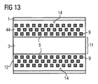
- 半導体層列(10)と、
フィルタ構造部(5)とを含み、
前記半導体層列(10)は、活性領域(45)とビーム出力結合面(12)を備え、前記ビーム出力結合面(12)は第1の部分領域(121)と、該第1の部分領域とは異なる第2の部分領域(122)を有している、レーザー光源において、
前記活性領域(45)は、作動モード中に、第1の波長領域のコヒーレントな第1の電磁ビーム(51)と、第2の波長領域のインコヒーレントな第2の電磁ビーム(52)とを生成し、
前記第2の波長領域は第1の波長領域を含んでおり、
前記コヒーレントな第1の電磁ビーム(51)は、第1の部分領域(121)から放射方向(90)に沿って放射され、
前記インコヒーレントな第2の電磁ビーム(52)は、第1の部分領域(121)と第2の部分領域(122)から放射され、
前記フィルタ構造部(5)は、活性領域から放射されたインコヒーレントな第2の電磁ビーム(52)を放射方向(90)に沿って少なくとも部分的に減衰するように構成されていることを特徴とするレーザー光源。 - 前記フィルタ構造部(5)は、放射方向(90)で見て半導体層列(10)の後方に配置された少なくとも1つの第1のフィルタ素子(6)を含んでいる、請求項1記載のレーザー光源。
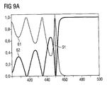
- 少なくとも1つの第1のフィルタ素子(6)は、電磁波ビームに対する角度依存性及び/又は波長依存性の透過性(61)を有しており、
前記第1のフィルタ素子(6)の透過性(61)は、放射方向(90)に対する角度(91)の増加と共に減衰し、及び/又は第1の波長領域からの偏差の増加と共に減衰する、請求項1または2記載のレーザー光源。 - 少なくとも1つの第1のフィルタ素子(6)は、ブラッグミラーを含んでいる、請求項1から3いずれか1項記載のレーザー光源。
- ブラッグミラーは、大域的な主要最大値と少なくとも1つの局所的な極大値を有する波長依存性の反射性を有し、
前記極大値は第1の波長領域にある、請求項1から4いずれか1項記載のレーザー光源。 - 前記少なくとも1つの第1のフィルタ素子(6)は、エタロンかまたは光学的バンドエッジフィルタを含んでいる、請求項3から5いずれか1項記載のレーザー光源。
- 前記半導体層列は分布帰還型レーザーとして構成されている、請求項3から6いずれか1項記載のレーザー光源。
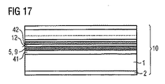
- 前記少なくとも1つの第1のフィルタ素子(6)は、電磁ビームに対して非透過性の材料を有する少なくとも1つの層を有し、
前記非透過性の材料は少なくとも部分的に第2の部分領域(122)上に配置されている、請求項3から7いずれか1項記載のレーザー光源。 - 少なくとも1つの層は、開口部を備えた孔部絞りとして構成されており、
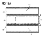
前記開口部は第1の部分領域(121)上に配置されている、請求項1から8いずれか1項記載のレーザー光源。 - 前記フィルタ構造部(5)は、少なくとも1つの第2のフィルタ素子(7)を含み、該第2のフィルタ素子(7)は半導体層列(10)のビーム出力結合面の一方に対向する表面(13)に配置されている、請求項1から9いずれか1項記載のレーザー光源。
- 少なくとも1つの第2のフィルタ素子(7)は、電磁ビームに対して角度依存性の透過性(61)を有し、
前記第2のフィルタ素子(7)の透過性(61)は放射方向(90)に対する角度の増加と共に増加している、請求項1から10いずれか1項記載のレーザー光源。 - 前記少なくとも1つの第2のフィルタ素子(7)は、ブラッグミラーを含んでいる、請求項10または11記載のレーザー光源。
- 前記フィルタ構造部(5)は、活性領域(45)が配置されている、コヒーレントな第1の電磁ビーム(51)に対する光共振器の少なくとも一部を形成している、請求項3から12いずれか1項記載のレーザー光源。
- コヒーレントな第1の電磁ビーム(51)は第1の強度を有し、インコヒーレントな第2の電磁ビーム(52)は、前記第1の強度よりも小さい第2の強度を有し、
少なくとも1つの第1のフィルタ素子(6)は、電磁ビームに対する強度依存性の透過性(61)を有し、
前記第1のフィルタ素子(6)は、第2の強度と同じかそれ以上の強度を有する電磁ビームに対して非透過性である、請求項1から13いずれか1項記載のレーザー光源。 - 少なくとも1つの第1のフィルタ素子(6)の電磁ビームに対する透過性(61)は、飽和特性を有している、請求項1から14いずれか1項記載のレーザー光源。
- 前記少なくとも1つの第1のフィルタ素子(6)は、コヒーレントな第1の電磁ビーム(51)のエネルギーよりも小さなバンドギャップを備えた半導体材料を有している、請求項14または15記載のレーザー光源。
- 少なくとも1つの第1のフィルタ素子(6)は、半導体材料を含んだ少なくとも1つの層を有している、請求項1から16いずれか1項記載のレーザー光源。
- 少なくとも1つの第1のフィルタ素子(6)は、2つの誘電層を有し、前記2つの誘電層の間には半導体材料を含んだ少なくとも1つの層が埋込まれている、請求項16または17記載のレーザー光源。
- 半導体材料を含んだ少なくとも1つの層は、半導体材料が含有された誘電マトリックス材料を有している、請求項16から18いずれか1項記載のレーザー光源。
- 前記少なくとも1つの第1のフィルタ素子(6)は、インコヒーレントな第2の電磁ビーム(52)の少なくとも一部を第3の波長領域(53)の電磁ビームに変換する、波長変換材料を有し、前記第3の波長領域と第2の波長領域は互いに異なっている、請求項14から19いずれか1項記載のレーザー光源。
- 前記フィルタ構造部(5)は、第1のフィルタ素子(6)の後方に配置される少なくとも1つの第3のフィルタ素子(8)を有し、
前記第3のフィルタ素子(8)は、第3の波長領域(53)を有する電磁ビームに対して非透過性である、請求項1から20いずれか1項記載のレーザー光源。 - 前記波長変換材料は、マトリックス材料の中に埋込まれている、請求項20または21記載のレーザー光源。
- コヒーレントな第1の電磁ビーム(51)は、少なくとも1つの第1のフィルタ素子の第1のフィルタ領域において第1の温度を発生し、
インコヒーレントな第2の電磁ビーム(52)は、少なくとも1つの第1のフィルタ素子の第2のフィルタ領域において第1の温度よりも低い第2の温度を発生し、
少なくとも1つの第1のフィルタ素子(6)は、電磁ビームに対して温度依存性の透過性(61)を有し、
少なくとも1つの第1のフィルタ素子(6)は、前記第2の温度と同じかそれ以上の温度までは非透過性である、請求項1から22いずれか1項記載のレーザー光源。 - 少なくとも1つの第1のフィルタ素子(6)は、アンチモン、銀、プラチナ、パラジウム、によって形成されるグループからなる少なくとも1つの元素を有している、請求項1から23いずれか1項記載のレーザー光源。
- 前記フィルタ構造部(5)は、少なくとも1つの第4のフィルタ素子(9)を有し、該第4のフィルタ素子は半導体層列(10)における放射方向(90)に対して並行な延在方向を有する面に配置されている、請求項1から24いずれか1項記載のレーザー光源。
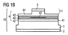
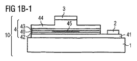
- 前記半導体層列(10)は、複数の層を有し、該複数の層のうちの1つの境界面が前記面である、請求項25記載のレーザー光源。
- 前記少なくとも1つの第4のフィルタ素子(9)は、半導体層列(10)の複数の層のうちの2つの層の間に配置されている、請求項25または26記載のレーザー光源。
- 前記少なくとも1つの第4のフィルタ素子(9)は、半導体層列(10)の外被層(5)として形成されている、請求項25から27いずれか1項記載のレーザー光源。
- 前記面は、半導体層列(10)におけるビーム出力結合面(12)とは異なる表面(14)である、請求項25記載のレーザー光源。
- 前記面は、半導体層列(10)の側面である、請求項25から29いずれか1項記載のレーザー光源。
- 前記少なくとも1つの第4のフィルタ素子(9)は、非透過性材料を備えた少なくとも1つの層を含んでいる、請求項25から30いずれか1項記載のレーザー光源。
- 前記少なくとも1つの第4のフィルタ素子(9)は、表面構造部を含んでいる、請求項25記載のレーザー光源。
- 前記半導体層列(10)は成長方向を有しており、表面構造部を備えた表面が、成長方向に対して垂直方向に配置されており、さらに表面構造部は活性領域(45)に対して横方向にずらされて配置されている、請求項32記載のレーザー光源。
- 前記表面構造部は、少なくとも1つの凹部若しくは凸部を有している、請求項32または33記載のレーザー光源。
- 前記表面構造部を備えた表面は、活性領域に向いた側か若しくは活性領域とは反対側の、基板(1)表面であるかまたは活性領域に向いた側若しくは活性領域とは反対側の、半導体層列(10)の電気的コンタクト層(2)の表面である、請求横32から34いずれか1項記載のレーザー光源。
- 前記少なくとも1つの凹部は、トレンチとして形成されている、請求項34または35記載のレーザー光源。
- 前記トレンチは延在方向を有しており、前記延在方向は、放射方向(90)と共に0°以上かつ90°以下の角度を形成している、請求項1から36いずれか1項記載のレーザー光源。
- 前記表面構造部は少なくとも部分的に非透過性材料で覆われる、請求項32から37いずれか1項記載のレーザー光源。
- 前記半導体層列(10)は2つの導波路層(42,43)を有し、該2つの導波路層(42,43)の間に活性領域(45)が設けられており、さらに表面構造部が表面から前記導波路層のうちの少なくとも1つ(43)へ延在している、請求項32から38いずれか1項記載のレーザー光源。
- 前記半導体層列(10)は、エッジ発光型半導体レーザーとして構成されている、請求項1から39いずれか1項記載のレーザー光源。
- 前記半導体層列(10)は、垂直発光型半導体レーザーとして構成されている、請求項1から39いずれか1項記載のレーザー光源。
- レーザー光源を製造するための方法において、
A)第1及び第2の部分領域(121,122)を有しているビーム出力結合面(12)と、作動モード中に前記第1の部分領域(121)から放射方向(90)に沿って放射される第1の波長領域を有するコヒーレントな第1の電磁ビーム(51)並びに前記第1の部分領域(121)と第2の部分領域(122)から放射される第2の波長領域を有するインコヒーレントな第2の電磁ビーム(52)を生成する活性領域(45)とを備えた半導体層列(10)を準備する方法ステップと、
B)前記第1及び第2の部分領域(121,122)上に非透過性材料からなる層を被着する方法ステップと、
C)第1の部分領域(121)上の非透過性材料を含んだ層を、酸素及び/又は窒素雰囲気において光化学反応及び/又は光熱反応の誘導によって透過性の層に変換する方法ステップとを有していることを特徴とする方法。 - 前記方法ステップC)がさらに以下の部分ステップ、すなわち、
コヒーレントな第1の電磁ビーム(51)とインコヒーレントな第2の電磁ビーム(42)を照射するために、半導体層列(10)を作動開始させる部分ステップが含まれている、請求項42記載の方法。 - 前記非透過性材料は、ケイ素、ガリウム、ゲルマニウム、アルミニウム、クロム、チタン、によって形成される群からなる少なくとも1つの材料を有している、請求項42または43記載の方法。
- 非透過性材料を含んだ層において、光化学反応による変換によって透過性の酸化物、窒化物または酸窒化物が第1の部分領域(121)上に形成される、請求項42から44いずれか1項記載の方法。
- 光熱反応による変換によって非透過性材料が第1の部分領域(121)上に蒸着される、請求項42から44いずれか一項記載の方法。
- さらなる方法ステップとして、
D)非透過性材料を含んだ層上に不活性化層を被着させる方法ステップが含まれる、請求項42から46いずれか一項記載の方法。 - 前記不活性化層は、酸化物、窒化物、又は酸窒化物を有している、請求項42から47いずれか一項記載の方法。
Applications Claiming Priority (3)
| Application Number | Priority Date | Filing Date | Title |
|---|---|---|---|
| DE102007061923 | 2007-12-21 | ||
| DE102008012859.7A DE102008012859B4 (de) | 2007-12-21 | 2008-03-06 | Laserlichtquelle mit einer Filterstruktur |
| PCT/DE2008/002127 WO2009080012A1 (de) | 2007-12-21 | 2008-12-17 | Laserlichtquelle und verfahren zur herstellung einer laserlichtquelle |
Related Child Applications (1)
| Application Number | Title | Priority Date | Filing Date |
|---|---|---|---|
| JP2015026613A Division JP6033902B2 (ja) | 2007-12-21 | 2015-02-13 | レーザー光源 |
Publications (2)
| Publication Number | Publication Date |
|---|---|
| JP2011507289A true JP2011507289A (ja) | 2011-03-03 |
| JP2011507289A5 JP2011507289A5 (ja) | 2012-07-12 |
Family
ID=40590023
Family Applications (3)
| Application Number | Title | Priority Date | Filing Date |
|---|---|---|---|
| JP2010538338A Pending JP2011507289A (ja) | 2007-12-21 | 2008-12-17 | レーザー光源及び該レーザー光源の製造方法 |
| JP2015026613A Active JP6033902B2 (ja) | 2007-12-21 | 2015-02-13 | レーザー光源 |
| JP2016209662A Pending JP2017017365A (ja) | 2007-12-21 | 2016-10-26 | レーザー光源及び該レーザー光源の製造方法 |
Family Applications After (2)
| Application Number | Title | Priority Date | Filing Date |
|---|---|---|---|
| JP2015026613A Active JP6033902B2 (ja) | 2007-12-21 | 2015-02-13 | レーザー光源 |
| JP2016209662A Pending JP2017017365A (ja) | 2007-12-21 | 2016-10-26 | レーザー光源及び該レーザー光源の製造方法 |
Country Status (7)
| Country | Link |
|---|---|
| US (6) | US8964808B2 (ja) |
| EP (1) | EP2223397B1 (ja) |
| JP (3) | JP2011507289A (ja) |
| KR (3) | KR101668218B1 (ja) |
| CN (2) | CN103107481B (ja) |
| DE (1) | DE102008012859B4 (ja) |
| WO (1) | WO2009080012A1 (ja) |
Cited By (5)
| Publication number | Priority date | Publication date | Assignee | Title |
|---|---|---|---|---|
| JP2013508965A (ja) * | 2009-10-27 | 2013-03-07 | ユニバーシティ オブ ソウル インダストリー コーポレーション ファウンデーション | 半導体デバイス |
| US8681411B2 (en) | 2009-08-21 | 2014-03-25 | University Of Seoul Industry Cooperation Foundation | Polariton mode optical switch with composite structure |
| US8748862B2 (en) | 2009-07-06 | 2014-06-10 | University Of Seoul Industry Cooperation Foundation | Compound semiconductors |
| US8802481B2 (en) | 2009-07-06 | 2014-08-12 | University Of Seoul Industry Cooperation Foundation | Photodetector capable of detecting the visible light spectrum |
| US8809834B2 (en) | 2009-07-06 | 2014-08-19 | University Of Seoul Industry Cooperation Foundation | Photodetector capable of detecting long wavelength radiation |
Families Citing this family (78)
| Publication number | Priority date | Publication date | Assignee | Title |
|---|---|---|---|---|
| DE102008012859B4 (de) | 2007-12-21 | 2023-10-05 | OSRAM Opto Semiconductors Gesellschaft mit beschränkter Haftung | Laserlichtquelle mit einer Filterstruktur |
| US8847249B2 (en) | 2008-06-16 | 2014-09-30 | Soraa, Inc. | Solid-state optical device having enhanced indium content in active regions |
| US8767787B1 (en) | 2008-07-14 | 2014-07-01 | Soraa Laser Diode, Inc. | Integrated laser diodes with quality facets on GaN substrates |
| US8805134B1 (en) | 2012-02-17 | 2014-08-12 | Soraa Laser Diode, Inc. | Methods and apparatus for photonic integration in non-polar and semi-polar oriented wave-guided optical devices |
| WO2010017148A1 (en) | 2008-08-04 | 2010-02-11 | Soraa, Inc. | White light devices using non-polar or semipolar gallium containing materials and phosphors |
| US8284810B1 (en) | 2008-08-04 | 2012-10-09 | Soraa, Inc. | Solid state laser device using a selected crystal orientation in non-polar or semi-polar GaN containing materials and methods |
| DE102008058436B4 (de) | 2008-11-21 | 2019-03-07 | Osram Opto Semiconductors Gmbh | Kantenemittierender Halbleiterlaserchip |
| US8247886B1 (en) | 2009-03-09 | 2012-08-21 | Soraa, Inc. | Polarization direction of optical devices using selected spatial configurations |
| US8634442B1 (en) | 2009-04-13 | 2014-01-21 | Soraa Laser Diode, Inc. | Optical device structure using GaN substrates for laser applications |
| US8837545B2 (en) | 2009-04-13 | 2014-09-16 | Soraa Laser Diode, Inc. | Optical device structure using GaN substrates and growth structures for laser applications |
| CN102396083B (zh) * | 2009-04-13 | 2015-12-16 | 天空激光二极管有限公司 | 用于激光器应用的使用gan衬底的光学装置结构 |
| US9829780B2 (en) | 2009-05-29 | 2017-11-28 | Soraa Laser Diode, Inc. | Laser light source for a vehicle |
| US8247887B1 (en) | 2009-05-29 | 2012-08-21 | Soraa, Inc. | Method and surface morphology of non-polar gallium nitride containing substrates |
| US8509275B1 (en) | 2009-05-29 | 2013-08-13 | Soraa, Inc. | Gallium nitride based laser dazzling device and method |
| US9250044B1 (en) | 2009-05-29 | 2016-02-02 | Soraa Laser Diode, Inc. | Gallium and nitrogen containing laser diode dazzling devices and methods of use |
| US8427590B2 (en) | 2009-05-29 | 2013-04-23 | Soraa, Inc. | Laser based display method and system |
| US10108079B2 (en) | 2009-05-29 | 2018-10-23 | Soraa Laser Diode, Inc. | Laser light source for a vehicle |
| DE102009035639B4 (de) | 2009-07-31 | 2019-10-24 | Osram Opto Semiconductors Gmbh | Breitstreifenlaser mit einem epitaktischen Schichtenstapel und Verfahren zu dessen Herstellung |
| DE102009028909A1 (de) | 2009-08-26 | 2011-03-17 | Nanoplus Gmbh Nanosystems And Technologies | Halbleiterlaser mit auf einem Laserspiegel angebrachtem Absorber |
| US8750342B1 (en) | 2011-09-09 | 2014-06-10 | Soraa Laser Diode, Inc. | Laser diodes with scribe structures |
| US9583678B2 (en) | 2009-09-18 | 2017-02-28 | Soraa, Inc. | High-performance LED fabrication |
| WO2011045797A1 (en) * | 2009-10-18 | 2011-04-21 | Technion- Research And Development Foundation Ltd. | A semiconductor two-photon device |
| US10147850B1 (en) | 2010-02-03 | 2018-12-04 | Soraa, Inc. | System and method for providing color light sources in proximity to predetermined wavelength conversion structures |
| US8905588B2 (en) | 2010-02-03 | 2014-12-09 | Sorra, Inc. | System and method for providing color light sources in proximity to predetermined wavelength conversion structures |
| DE102010015197A1 (de) * | 2010-04-16 | 2012-01-19 | Osram Opto Semiconductors Gmbh | Laserlichtquelle |
| DE102010020625B4 (de) | 2010-05-14 | 2024-02-22 | OSRAM Opto Semiconductors Gesellschaft mit beschränkter Haftung | Verfahren zur Herstellung eines kantenemittierenden Halbleiterlasers |
| US8451876B1 (en) | 2010-05-17 | 2013-05-28 | Soraa, Inc. | Method and system for providing bidirectional light sources with broad spectrum |
| US9450143B2 (en) | 2010-06-18 | 2016-09-20 | Soraa, Inc. | Gallium and nitrogen containing triangular or diamond-shaped configuration for optical devices |
| US8816319B1 (en) | 2010-11-05 | 2014-08-26 | Soraa Laser Diode, Inc. | Method of strain engineering and related optical device using a gallium and nitrogen containing active region |
| US9048170B2 (en) | 2010-11-09 | 2015-06-02 | Soraa Laser Diode, Inc. | Method of fabricating optical devices using laser treatment |
| US9595813B2 (en) | 2011-01-24 | 2017-03-14 | Soraa Laser Diode, Inc. | Laser package having multiple emitters configured on a substrate member |
| US9025635B2 (en) | 2011-01-24 | 2015-05-05 | Soraa Laser Diode, Inc. | Laser package having multiple emitters configured on a support member |
| US9093820B1 (en) | 2011-01-25 | 2015-07-28 | Soraa Laser Diode, Inc. | Method and structure for laser devices using optical blocking regions |
| US9287684B2 (en) | 2011-04-04 | 2016-03-15 | Soraa Laser Diode, Inc. | Laser package having multiple emitters with color wheel |
| DE102011100175B4 (de) | 2011-05-02 | 2021-12-23 | OSRAM Opto Semiconductors Gesellschaft mit beschränkter Haftung | Laserlichtquelle mit einer Stegwellenleiterstruktur und einer Modenfilterstruktur |
| US8686431B2 (en) | 2011-08-22 | 2014-04-01 | Soraa, Inc. | Gallium and nitrogen containing trilateral configuration for optical devices |
| DE102011111604B4 (de) | 2011-08-25 | 2023-01-19 | OSRAM Opto Semiconductors Gesellschaft mit beschränkter Haftung | Strahlungsemittierendes Halbleiterbauelement |
| US8971370B1 (en) | 2011-10-13 | 2015-03-03 | Soraa Laser Diode, Inc. | Laser devices using a semipolar plane |
| DE102011054954A1 (de) | 2011-10-31 | 2013-05-02 | Osram Opto Semiconductors Gmbh | Verfahren zur Herstellung eines optoelektronischen Halbleiterbauteils und optoelektronischer Halbleiterlaser |
| US9020003B1 (en) | 2012-03-14 | 2015-04-28 | Soraa Laser Diode, Inc. | Group III-nitride laser diode grown on a semi-polar orientation of gallium and nitrogen containing substrates |
| US9343871B1 (en) | 2012-04-05 | 2016-05-17 | Soraa Laser Diode, Inc. | Facet on a gallium and nitrogen containing laser diode |
| DE102012103549B4 (de) | 2012-04-23 | 2020-06-18 | Osram Opto Semiconductors Gmbh | Halbleiterlaserlichtquelle mit einem kantenemittierenden Halbleiterkörper und Licht streuenden Teilbereich |
| DE102012106943B4 (de) * | 2012-07-30 | 2019-06-27 | Osram Opto Semiconductors Gmbh | Verfahren zur Herstellung einer Halbleiterlaserdiode und Halbleiterlaserdiode |
| DE102012109175B4 (de) * | 2012-09-27 | 2019-02-28 | Osram Opto Semiconductors Gmbh | Halbleiterlaserdiode |
| US9978904B2 (en) | 2012-10-16 | 2018-05-22 | Soraa, Inc. | Indium gallium nitride light emitting devices |
| DE102012110613A1 (de) * | 2012-11-06 | 2014-05-08 | Osram Opto Semiconductors Gmbh | Optoelektronisches Halbleiterbauelement |
| JP6142429B2 (ja) * | 2013-02-28 | 2017-06-07 | 京セラ株式会社 | エタロン及びエタロン装置 |
| DE102013102328A1 (de) | 2013-03-08 | 2014-09-11 | Osram Opto Semiconductors Gmbh | Halbleiterlaseranordnung |
| DE102013105798A1 (de) * | 2013-06-05 | 2014-12-11 | Osram Opto Semiconductors Gmbh | Optoelektronisches Halbleiterbauteil |
| US9419189B1 (en) | 2013-11-04 | 2016-08-16 | Soraa, Inc. | Small LED source with high brightness and high efficiency |
| KR20150059835A (ko) * | 2013-11-25 | 2015-06-03 | 에스케이하이닉스 주식회사 | 관통전극을 갖는 반도체 소자 |
| US10191213B2 (en) | 2014-01-09 | 2019-01-29 | Globalfoundries Inc. | Shielding structures between optical waveguides |
| KR20160139022A (ko) | 2014-04-09 | 2016-12-06 | 후아웨이 테크놀러지 컴퍼니 리미티드 | 에지 결합 장치 제조 |
| DE102015110496B4 (de) * | 2015-06-30 | 2018-06-14 | Infineon Technologies Dresden Gmbh | Integriertes, lichtemittierendes bauelement,integriertes sensorbauelement undherstellungsverfahren |
| WO2017046023A1 (en) | 2015-09-14 | 2017-03-23 | University College Cork | Semi-metal rectifying junction |
| US9787963B2 (en) | 2015-10-08 | 2017-10-10 | Soraa Laser Diode, Inc. | Laser lighting having selective resolution |
| US9837792B2 (en) * | 2016-03-07 | 2017-12-05 | Epistar Corporation | Light-emitting device |
| DE102016106495A1 (de) * | 2016-04-08 | 2017-10-12 | Osram Opto Semiconductors Gmbh | Halbleiterlaser |
| DE102016111442A1 (de) * | 2016-06-22 | 2017-12-28 | Osram Opto Semiconductors Gmbh | Halbleiterlichtquelle |
| DE102016113071A1 (de) * | 2016-07-15 | 2018-01-18 | Osram Opto Semiconductors Gmbh | Halbleiterlaserdiode |
| TWI609541B (zh) * | 2016-12-12 | 2017-12-21 | 聯亞光電工業股份有限公司 | 半導體雷射裝置 |
| DE102017100997A1 (de) * | 2017-01-19 | 2018-07-19 | Osram Opto Semiconductors Gmbh | Halbleiterlaser und Verfahren zur Herstellung eines solchen Halbleiterlasers |
| US20180278011A1 (en) | 2017-03-23 | 2018-09-27 | Infineon Technologies Ag | Laser diode module |
| US10771155B2 (en) | 2017-09-28 | 2020-09-08 | Soraa Laser Diode, Inc. | Intelligent visible light with a gallium and nitrogen containing laser source |
| US10222474B1 (en) | 2017-12-13 | 2019-03-05 | Soraa Laser Diode, Inc. | Lidar systems including a gallium and nitrogen containing laser light source |
| US10551728B1 (en) | 2018-04-10 | 2020-02-04 | Soraa Laser Diode, Inc. | Structured phosphors for dynamic lighting |
| DE102018125493A1 (de) * | 2018-10-15 | 2020-04-16 | Osram Opto Semiconductors Gmbh | Kantenemittierender halbleiterlaser und verfahren zur herstellung eines kantenemittierenden halbleiterlasers |
| US11421843B2 (en) | 2018-12-21 | 2022-08-23 | Kyocera Sld Laser, Inc. | Fiber-delivered laser-induced dynamic light system |
| US11239637B2 (en) | 2018-12-21 | 2022-02-01 | Kyocera Sld Laser, Inc. | Fiber delivered laser induced white light system |
| US11884202B2 (en) | 2019-01-18 | 2024-01-30 | Kyocera Sld Laser, Inc. | Laser-based fiber-coupled white light system |
| US11588290B2 (en) * | 2019-12-30 | 2023-02-21 | Raytheon Company | Methods and apparatus for generating ghost light |
| US11245250B2 (en) | 2020-04-20 | 2022-02-08 | Cisco Technology, Inc. | Quantum dot comb laser |
| CN111641102B (zh) * | 2020-05-20 | 2022-01-11 | 深圳瑞波光电子有限公司 | 半导体激光器、巴条及制作方法 |
| DE102020118824A1 (de) | 2020-07-16 | 2022-01-20 | OSRAM Opto Semiconductors Gesellschaft mit beschränkter Haftung | Optoelektronisches halbleiterbauelement, verfahren zur herstellung des optoelektronischen halbleiterbauelements und lidar-system |
| US20220344905A1 (en) * | 2021-04-21 | 2022-10-27 | Osram Opto Semiconductors Gmbh | Semiconductor laser device and projection device |
| DE102021121115A1 (de) * | 2021-08-13 | 2023-02-16 | OSRAM Opto Semiconductors Gesellschaft mit beschränkter Haftung | Spiegel für einen laser, laser und laserbauteil |
| KR102513576B1 (ko) * | 2021-09-02 | 2023-03-29 | 주식회사 루트로닉 | 레이저 장치 |
| DE102022104418A1 (de) | 2022-02-24 | 2023-08-24 | Ams-Osram International Gmbh | Kantenemittierende halbleiterlaserdiode |
Citations (6)
| Publication number | Priority date | Publication date | Assignee | Title |
|---|---|---|---|---|
| JPS5543884A (en) * | 1978-09-22 | 1980-03-27 | Fujitsu Ltd | Semiconductor light emission device |
| JPH01244431A (ja) * | 1988-03-25 | 1989-09-28 | Nec Corp | 可変波長フィルタ |
| JP2001068784A (ja) * | 1999-02-17 | 2001-03-16 | Matsushita Electric Ind Co Ltd | 半導体レーザ装置、光ディスク装置及び光集積化装置 |
| JP2003091875A (ja) * | 2001-07-09 | 2003-03-28 | Ricoh Co Ltd | 相変化型光情報記録媒体、光情報記録再生装置及び方法、並びに光学フィルター |
| JP2003198065A (ja) * | 2001-12-26 | 2003-07-11 | Sharp Corp | 窒化物半導体レーザ素子および光記録再生装置 |
| JP2004083653A (ja) * | 2002-08-23 | 2004-03-18 | Sharp Corp | 発光装置ならびに蛍光体およびその製造方法 |
Family Cites Families (45)
| Publication number | Priority date | Publication date | Assignee | Title |
|---|---|---|---|---|
| JPS57113643A (en) | 1981-01-05 | 1982-07-15 | Toshiba Corp | Optical transmission system using semiconductor laser |
| JPH067625B2 (ja) | 1985-01-28 | 1994-01-26 | キヤノン株式会社 | モニタ−用光検出器内蔵半導体レ−ザ素子 |
| JP2659187B2 (ja) | 1987-04-14 | 1997-09-30 | 日本電気株式会社 | 光フィルタ素子 |
| JPH08264890A (ja) * | 1995-03-28 | 1996-10-11 | Alps Electric Co Ltd | 分布帰還型半導体レーザおよびその製造方法 |
| JPH11511298A (ja) | 1995-08-29 | 1999-09-28 | シーメンス アクチエンゲゼルシヤフト | レーザ装置 |
| US6044101A (en) | 1995-08-29 | 2000-03-28 | Siemens Aktiengesellschaft | Semiconductor laser device |
| JPH09167873A (ja) | 1995-12-15 | 1997-06-24 | Mitsubishi Electric Corp | 半導体レーザ装置 |
| US5923690A (en) | 1996-01-25 | 1999-07-13 | Matsushita Electric Industrial Co., Ltd. | Semiconductor laser device |
| JP2003142780A (ja) | 1996-01-25 | 2003-05-16 | Matsushita Electric Ind Co Ltd | 半導体レーザ装置 |
| JPH1098235A (ja) * | 1996-08-01 | 1998-04-14 | Pioneer Electron Corp | 無再成長分布帰還リッジ型半導体レーザ及びその製造方法 |
| WO2000046862A1 (fr) | 1999-02-05 | 2000-08-10 | Japan Energy Corporation | Element fonctionnel de conversion photoelectrique et procede de fabrication correspondant |
| US7212556B1 (en) | 1999-02-17 | 2007-05-01 | Matsushita Electric Industrial Co., Ltd. | Semiconductor laser device optical disk apparatus and optical integrated unit |
| JP2001135885A (ja) | 1999-11-04 | 2001-05-18 | Matsushita Electric Ind Co Ltd | 半導体レーザ装置及びその組立方法 |
| US6835963B2 (en) | 1999-12-22 | 2004-12-28 | Kabushiki Kaisha Toshiba | Light-emitting element and method of fabrication thereof |
| JP4160226B2 (ja) | 1999-12-28 | 2008-10-01 | 株式会社東芝 | 半導体レーザ装置 |
| US6693935B2 (en) | 2000-06-20 | 2004-02-17 | Sony Corporation | Semiconductor laser |
| JP2002006595A (ja) * | 2000-06-21 | 2002-01-09 | Hitachi Ltd | 電子写真装置 |
| US20020024828A1 (en) | 2000-08-31 | 2002-02-28 | Hidetake Hayashi | Inverter suitable for use with portable AC power supply unit |
| JP2002280663A (ja) | 2001-03-15 | 2002-09-27 | Sony Corp | 半導体レーザ素子及び光集積デバイス |
| CA2449047C (en) | 2001-05-31 | 2012-01-31 | Nichia Corporation | Semiconductor laser element with shading layers and improved far field pattern |
| US7042830B2 (en) | 2001-07-09 | 2006-05-09 | Ricoh Company, Ltd. | Phase-change optical information recording medium, and optical information recording and reproducing apparatus and method for the same |
| US20030021327A1 (en) * | 2001-07-25 | 2003-01-30 | Murry Stefan J. | Semiconductor surface-emitting laser with integrated photodetector |
| US20050040410A1 (en) | 2002-02-12 | 2005-02-24 | Nl-Nanosemiconductor Gmbh | Tilted cavity semiconductor optoelectronic device and method of making same |
| ATE360274T1 (de) * | 2002-12-02 | 2007-05-15 | Newport Corp | Laser mit externem resonator und verbessertem einzelmodenbetrieb |
| WO2004081610A2 (en) | 2003-03-14 | 2004-09-23 | Pbc Lasers Ltd. | Apparatus for generating improved laser beam |
| KR20050019485A (ko) | 2003-08-19 | 2005-03-03 | 삼성전자주식회사 | 광검출소자가 일체적으로 형성되는 수직 면발광 레이저 |
| WO2005041371A1 (en) | 2003-09-30 | 2005-05-06 | Pirelli & C. S.P.A. | Phase-control in an external-cavity tuneable laser |
| JP4830315B2 (ja) * | 2004-03-05 | 2011-12-07 | 日亜化学工業株式会社 | 半導体レーザ素子 |
| JP2005260023A (ja) * | 2004-03-12 | 2005-09-22 | Fuji Photo Film Co Ltd | 半導体レーザ素子 |
| US7403553B2 (en) * | 2004-06-25 | 2008-07-22 | Finisar Corporation | Absorbing layers for reduced spontaneous emission effects in an integrated photodiode |
| JP4425740B2 (ja) | 2004-08-02 | 2010-03-03 | 富士通株式会社 | 光増幅器 |
| WO2006035388A2 (en) | 2004-09-30 | 2006-04-06 | Koninklijke Philips Electronics N.V. | Phosphor-converted led with luminance enhancement through light recycling |
| JP2006100626A (ja) * | 2004-09-30 | 2006-04-13 | Fuji Photo Film Co Ltd | 半導体発光装置 |
| JP4451371B2 (ja) | 2004-12-20 | 2010-04-14 | シャープ株式会社 | 窒化物半導体レーザ素子 |
| KR100674836B1 (ko) | 2005-02-28 | 2007-01-26 | 삼성전기주식회사 | 고출력 단일모드 반도체 레이저소자 및 그 제조방법 |
| JP2006278458A (ja) * | 2005-03-28 | 2006-10-12 | Sharp Corp | 発光素子とその製造方法および照明装置 |
| US7399953B2 (en) | 2005-05-06 | 2008-07-15 | Avago Technologies Ecbu Ip Pte Ltd | Light source control in optical pointing device |
| JP4842827B2 (ja) * | 2005-05-19 | 2011-12-21 | パナソニック株式会社 | 窒化物半導体装置及びその製造方法 |
| US8206611B2 (en) * | 2005-05-24 | 2012-06-26 | Mitsubishi Chemical Corporation | Phosphor and use thereof |
| JP2007027207A (ja) * | 2005-07-12 | 2007-02-01 | Sumitomo Electric Ind Ltd | 半導体発光素子 |
| DE102005058237A1 (de) | 2005-09-30 | 2007-04-05 | Osram Opto Semiconductors Gmbh | Oberflächenemittierendes Halbleiterlaser-Bauelement und optische Projektionsvorrichtung mit solch einem oberflächenemittierenden Halbleiterlaser-Bauelement |
| DE102005056949B4 (de) | 2005-09-30 | 2013-08-22 | Osram Opto Semiconductors Gmbh | Optisch gepumpter oberflächenemittierender Halbleiterlaser und optische Projektionsvorrichtung mit solch einem Halbleiterlaser |
| DE102006010728A1 (de) | 2005-12-05 | 2007-06-06 | Osram Opto Semiconductors Gmbh | Halbleiterbauelement und Laservorrichtung |
| JP5135717B2 (ja) | 2006-05-31 | 2013-02-06 | ソニー株式会社 | 半導体発光装置 |
| DE102008012859B4 (de) * | 2007-12-21 | 2023-10-05 | OSRAM Opto Semiconductors Gesellschaft mit beschränkter Haftung | Laserlichtquelle mit einer Filterstruktur |
-
2008
- 2008-03-06 DE DE102008012859.7A patent/DE102008012859B4/de active Active
- 2008-12-17 WO PCT/DE2008/002127 patent/WO2009080012A1/de active Application Filing
- 2008-12-17 CN CN201310049689.2A patent/CN103107481B/zh active Active
- 2008-12-17 JP JP2010538338A patent/JP2011507289A/ja active Pending
- 2008-12-17 KR KR1020167005096A patent/KR101668218B1/ko active IP Right Grant
- 2008-12-17 KR KR1020157002077A patent/KR101580436B1/ko active IP Right Grant
- 2008-12-17 EP EP08865674.9A patent/EP2223397B1/de active Active
- 2008-12-17 US US13/730,363 patent/US8964808B2/en active Active
- 2008-12-17 KR KR1020107016285A patent/KR101600633B1/ko active Application Filing
- 2008-12-17 US US12/809,748 patent/US8369370B2/en active Active
- 2008-12-17 CN CN2008801272114A patent/CN101946378B/zh active Active
-
2015
- 2015-02-13 JP JP2015026613A patent/JP6033902B2/ja active Active
- 2015-02-20 US US14/627,895 patent/US9407063B2/en active Active
- 2015-11-24 US US14/951,096 patent/US9531158B2/en active Active
- 2015-11-24 US US14/951,220 patent/US9559497B2/en active Active
- 2015-11-24 US US14/951,149 patent/US9559496B2/en active Active
-
2016
- 2016-10-26 JP JP2016209662A patent/JP2017017365A/ja active Pending
Patent Citations (6)
| Publication number | Priority date | Publication date | Assignee | Title |
|---|---|---|---|---|
| JPS5543884A (en) * | 1978-09-22 | 1980-03-27 | Fujitsu Ltd | Semiconductor light emission device |
| JPH01244431A (ja) * | 1988-03-25 | 1989-09-28 | Nec Corp | 可変波長フィルタ |
| JP2001068784A (ja) * | 1999-02-17 | 2001-03-16 | Matsushita Electric Ind Co Ltd | 半導体レーザ装置、光ディスク装置及び光集積化装置 |
| JP2003091875A (ja) * | 2001-07-09 | 2003-03-28 | Ricoh Co Ltd | 相変化型光情報記録媒体、光情報記録再生装置及び方法、並びに光学フィルター |
| JP2003198065A (ja) * | 2001-12-26 | 2003-07-11 | Sharp Corp | 窒化物半導体レーザ素子および光記録再生装置 |
| JP2004083653A (ja) * | 2002-08-23 | 2004-03-18 | Sharp Corp | 発光装置ならびに蛍光体およびその製造方法 |
Cited By (6)
| Publication number | Priority date | Publication date | Assignee | Title |
|---|---|---|---|---|
| US8748862B2 (en) | 2009-07-06 | 2014-06-10 | University Of Seoul Industry Cooperation Foundation | Compound semiconductors |
| US8802481B2 (en) | 2009-07-06 | 2014-08-12 | University Of Seoul Industry Cooperation Foundation | Photodetector capable of detecting the visible light spectrum |
| US8809834B2 (en) | 2009-07-06 | 2014-08-19 | University Of Seoul Industry Cooperation Foundation | Photodetector capable of detecting long wavelength radiation |
| US9397249B2 (en) | 2009-07-06 | 2016-07-19 | University Of Seoul Industry Cooperation Foundation | Photodetector capable of detecting long wavelength radiation |
| US8681411B2 (en) | 2009-08-21 | 2014-03-25 | University Of Seoul Industry Cooperation Foundation | Polariton mode optical switch with composite structure |
| JP2013508965A (ja) * | 2009-10-27 | 2013-03-07 | ユニバーシティ オブ ソウル インダストリー コーポレーション ファウンデーション | 半導体デバイス |
Also Published As
| Publication number | Publication date |
|---|---|
| WO2009080012A1 (de) | 2009-07-02 |
| US20150162722A1 (en) | 2015-06-11 |
| KR20160027256A (ko) | 2016-03-09 |
| KR101600633B1 (ko) | 2016-03-07 |
| US8964808B2 (en) | 2015-02-24 |
| JP2017017365A (ja) | 2017-01-19 |
| CN101946378B (zh) | 2013-03-27 |
| KR20150017774A (ko) | 2015-02-17 |
| EP2223397B1 (de) | 2019-01-30 |
| US9531158B2 (en) | 2016-12-27 |
| US20160079734A1 (en) | 2016-03-17 |
| DE102008012859A1 (de) | 2009-11-19 |
| US20110188530A1 (en) | 2011-08-04 |
| KR101580436B1 (ko) | 2015-12-24 |
| CN103107481A (zh) | 2013-05-15 |
| US9407063B2 (en) | 2016-08-02 |
| US9559497B2 (en) | 2017-01-31 |
| US8369370B2 (en) | 2013-02-05 |
| CN101946378A (zh) | 2011-01-12 |
| US9559496B2 (en) | 2017-01-31 |
| DE102008012859B4 (de) | 2023-10-05 |
| EP2223397A1 (de) | 2010-09-01 |
| KR20100102675A (ko) | 2010-09-24 |
| JP2015111724A (ja) | 2015-06-18 |
| US20160087404A1 (en) | 2016-03-24 |
| US20130148683A1 (en) | 2013-06-13 |
| JP6033902B2 (ja) | 2016-11-30 |
| US20160079733A1 (en) | 2016-03-17 |
| KR101668218B1 (ko) | 2016-10-20 |
| CN103107481B (zh) | 2015-10-28 |
Similar Documents
| Publication | Publication Date | Title |
|---|---|---|
| JP6033902B2 (ja) | レーザー光源 | |
| US8306084B2 (en) | Laser light source | |
| US5793062A (en) | Transparent substrate light emitting diodes with directed light output | |
| US5966399A (en) | Vertical cavity surface emitting laser with integrated diffractive lens and method of fabrication | |
| US6015719A (en) | Transparent substrate light emitting diodes with directed light output | |
| TWI475773B (zh) | 垂直腔表面發射雷射 | |
| JPH09172227A (ja) | 光電子量子井戸装置 | |
| JP2007533126A (ja) | 反導波路傾斜空洞型vcselまたはled | |
| US6947460B2 (en) | Optically pumpable surface-emitting semiconductor laser device | |
| US20070091953A1 (en) | Light-emitting diode with a narrow beam divergence based on the effect of photonic band crystal-mediated filtration of high-order optical modes | |
| US20060018354A1 (en) | Optically pumped surface emitting semiconductor laser device | |
| US20230126297A1 (en) | Semiconductor laser and lidar system comprising the semiconductor laser | |
| JPH08236807A (ja) | 半導体発光素子及び半導体発光素子アレイチップ | |
| WO2023151908A1 (en) | Laser diode component | |
| KR100269145B1 (ko) | 표면광레이저다이오드및그제조방법 | |
| JPH0980362A (ja) | 光ゲート素子 |
Legal Events
| Date | Code | Title | Description |
|---|---|---|---|
| RD04 | Notification of resignation of power of attorney |
Free format text: JAPANESE INTERMEDIATE CODE: A7424 Effective date: 20101228 |
|
| A521 | Request for written amendment filed |
Free format text: JAPANESE INTERMEDIATE CODE: A523 Effective date: 20111031 |
|
| A621 | Written request for application examination |
Free format text: JAPANESE INTERMEDIATE CODE: A621 Effective date: 20111031 |
|
| A521 | Request for written amendment filed |
Free format text: JAPANESE INTERMEDIATE CODE: A523 Effective date: 20120528 |
|
| A977 | Report on retrieval |
Free format text: JAPANESE INTERMEDIATE CODE: A971007 Effective date: 20130228 |
|
| A131 | Notification of reasons for refusal |
Free format text: JAPANESE INTERMEDIATE CODE: A131 Effective date: 20130306 |
|
| A601 | Written request for extension of time |
Free format text: JAPANESE INTERMEDIATE CODE: A601 Effective date: 20130604 |
|
| A602 | Written permission of extension of time |
Free format text: JAPANESE INTERMEDIATE CODE: A602 Effective date: 20130611 |
|
| A521 | Request for written amendment filed |
Free format text: JAPANESE INTERMEDIATE CODE: A523 Effective date: 20130705 |
|
| A131 | Notification of reasons for refusal |
Free format text: JAPANESE INTERMEDIATE CODE: A131 Effective date: 20131118 |
|
| A601 | Written request for extension of time |
Free format text: JAPANESE INTERMEDIATE CODE: A601 Effective date: 20140205 |
|
| A602 | Written permission of extension of time |
Free format text: JAPANESE INTERMEDIATE CODE: A602 Effective date: 20140213 |
|
| A521 | Request for written amendment filed |
Free format text: JAPANESE INTERMEDIATE CODE: A523 Effective date: 20140515 |
|
| A02 | Decision of refusal |
Free format text: JAPANESE INTERMEDIATE CODE: A02 Effective date: 20141014 |
|
| A521 | Request for written amendment filed |
Free format text: JAPANESE INTERMEDIATE CODE: A523 Effective date: 20150213 |
|
| A911 | Transfer to examiner for re-examination before appeal (zenchi) |
Free format text: JAPANESE INTERMEDIATE CODE: A911 Effective date: 20150220 |
|
| A912 | Re-examination (zenchi) completed and case transferred to appeal board |
Free format text: JAPANESE INTERMEDIATE CODE: A912 Effective date: 20150501 |