JP2010212509A5 - - Google Patents
Download PDFInfo
- Publication number
- JP2010212509A5 JP2010212509A5 JP2009058409A JP2009058409A JP2010212509A5 JP 2010212509 A5 JP2010212509 A5 JP 2010212509A5 JP 2009058409 A JP2009058409 A JP 2009058409A JP 2009058409 A JP2009058409 A JP 2009058409A JP 2010212509 A5 JP2010212509 A5 JP 2010212509A5
- Authority
- JP
- Japan
- Prior art keywords
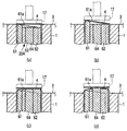
- semiconductor chip
- push
- picking
- adhesive sheet
- upward direction
- Prior art date
- Legal status (The legal status is an assumption and is not a legal conclusion. Google has not performed a legal analysis and makes no representation as to the accuracy of the status listed.)
- Granted
Links
- 239000004065 semiconductor Substances 0.000 claims description 49
- 239000000853 adhesive Substances 0.000 claims description 10
- 230000001070 adhesive effect Effects 0.000 claims description 10
- 239000002390 adhesive tape Substances 0.000 claims description 9
- 239000004820 Pressure-sensitive adhesive Substances 0.000 claims description 3
- 230000001174 ascending effect Effects 0.000 claims description 2
- 238000000034 method Methods 0.000 claims description 2
- 230000002093 peripheral effect Effects 0.000 claims description 2
Images


Priority Applications (1)
| Application Number | Priority Date | Filing Date | Title |
|---|---|---|---|
| JP2009058409A JP5284144B2 (ja) | 2009-03-11 | 2009-03-11 | 半導体チップのピックアップ装置及びピックアップ方法 |
Applications Claiming Priority (1)
| Application Number | Priority Date | Filing Date | Title |
|---|---|---|---|
| JP2009058409A JP5284144B2 (ja) | 2009-03-11 | 2009-03-11 | 半導体チップのピックアップ装置及びピックアップ方法 |
Publications (3)
| Publication Number | Publication Date |
|---|---|
| JP2010212509A JP2010212509A (ja) | 2010-09-24 |
| JP2010212509A5 true JP2010212509A5 (OSRAM) | 2013-04-18 |
| JP5284144B2 JP5284144B2 (ja) | 2013-09-11 |
Family
ID=42972371
Family Applications (1)
| Application Number | Title | Priority Date | Filing Date |
|---|---|---|---|
| JP2009058409A Active JP5284144B2 (ja) | 2009-03-11 | 2009-03-11 | 半導体チップのピックアップ装置及びピックアップ方法 |
Country Status (1)
| Country | Link |
|---|---|
| JP (1) | JP5284144B2 (OSRAM) |
Families Citing this family (13)
| Publication number | Priority date | Publication date | Assignee | Title |
|---|---|---|---|---|
| KR101186799B1 (ko) | 2012-01-26 | 2012-09-28 | 한국기계연구원 | 반도체 칩 픽업 장치 |
| KR101397750B1 (ko) * | 2012-07-25 | 2014-05-21 | 삼성전기주식회사 | 칩 이젝터 및 이를 이용한 칩 탈착 방법 |
| JP6366223B2 (ja) * | 2013-02-25 | 2018-08-01 | 東レエンジニアリング株式会社 | 半導体チップのピックアップ装置 |
| JP6200735B2 (ja) * | 2013-09-09 | 2017-09-20 | ファスフォードテクノロジ株式会社 | ダイボンダ及びボンディング方法 |
| KR101585316B1 (ko) * | 2014-01-29 | 2016-01-13 | 세메스 주식회사 | 다이 이젝팅 장치 |
| JP6368407B2 (ja) * | 2016-08-04 | 2018-08-01 | 日本ファインテック株式会社 | チップ剥離装置及びチップ剥離方法 |
| JP7217605B2 (ja) * | 2018-09-21 | 2023-02-03 | ファスフォードテクノロジ株式会社 | 半導体製造装置、突上げ治具および半導体装置の製造方法 |
| WO2020178889A1 (ja) * | 2019-03-01 | 2020-09-10 | 株式会社Fuji | 電子部品剥離装置及び電子部品の剥離方法 |
| JP7377654B2 (ja) * | 2019-09-17 | 2023-11-10 | ファスフォードテクノロジ株式会社 | ダイボンディング装置、剥離ユニット、コレットおよび半導体装置の製造方法 |
| JP7612428B2 (ja) * | 2020-03-23 | 2025-01-14 | ファスフォードテクノロジ株式会社 | ダイボンディング装置、剥離治具および半導体装置の製造方法 |
| KR102617784B1 (ko) * | 2020-07-09 | 2023-12-26 | 세메스 주식회사 | 다이 이젝터 및 이를 포함하는 다이 본딩 장치 |
| JP7645768B2 (ja) * | 2021-10-26 | 2025-03-14 | 三菱電機株式会社 | 半導体製造装置および半導体装置の製造方法 |
| JP7655216B2 (ja) * | 2021-12-20 | 2025-04-02 | 三菱電機株式会社 | 半導体製造装置 |
Family Cites Families (6)
| Publication number | Priority date | Publication date | Assignee | Title |
|---|---|---|---|---|
| JP2000353710A (ja) * | 1999-06-14 | 2000-12-19 | Toshiba Corp | ペレットピックアップ装置および半導体装置の製造方法 |
| JP4574251B2 (ja) * | 2003-09-17 | 2010-11-04 | ルネサスエレクトロニクス株式会社 | 半導体装置の製造方法 |
| JP2005322815A (ja) * | 2004-05-11 | 2005-11-17 | Matsushita Electric Ind Co Ltd | 半導体製造装置および半導体装置の製造方法 |
| JP4616748B2 (ja) * | 2005-10-11 | 2011-01-19 | 株式会社新川 | ダイピックアップ装置 |
| JP2008141068A (ja) * | 2006-12-04 | 2008-06-19 | Shibaura Mechatronics Corp | 半導体チップのピックアップ装置及びピックアップ方法 |
| JP4752790B2 (ja) * | 2007-02-26 | 2011-08-17 | パナソニック株式会社 | 電子部品のピックアップ方法とそれに用いるピックアップ装置 |
-
2009
- 2009-03-11 JP JP2009058409A patent/JP5284144B2/ja active Active
Similar Documents
| Publication | Publication Date | Title |
|---|---|---|
| JP2010212509A5 (OSRAM) | ||
| KR101596461B1 (ko) | 칩 디테칭 장치 및 칩 디테칭 방법 | |
| KR102084792B1 (ko) | 포일로부터 반도체 칩을 탈착시키기 위한 방법 | |
| US9272839B2 (en) | Glass panel packaging box and de-packaging method thereof | |
| EP1864922A3 (de) | Verfahren zum Abheben der obersten Kunstoffplatte von einem Plattenstapel und Vorrichtung zum Abheben der obersten Kunstoffplatte | |
| JP5284144B2 (ja) | 半導体チップのピックアップ装置及びピックアップ方法 | |
| EP1617463A3 (en) | Film peeling method and film peeling device | |
| JP2017519648A5 (OSRAM) | ||
| WO2010011088A3 (ko) | 솔라셀 패널 제조장치 및 제조방법 | |
| JP2018182278A5 (OSRAM) | ||
| JP4816598B2 (ja) | チップ剥離装置およびチップ剥離方法ならびにチップピックアップ装置 | |
| JP4765536B2 (ja) | チップピックアップ装置およびチップピックアップ方法ならびにチップ剥離装置およびチップ剥離方法 | |
| JP2019029650A5 (OSRAM) | ||
| US9302892B1 (en) | Toilet lifting device | |
| JP2012508460A5 (OSRAM) | ||
| JP5214421B2 (ja) | 剥離装置及び剥離方法 | |
| TWI353957B (OSRAM) | ||
| JP2013168616A (ja) | 保護テープ剥離方法 | |
| KR101322571B1 (ko) | 반도체 소자들을 픽업하기 위한 장치 | |
| TWI590362B (zh) | 拾取裝置 | |
| JP2014165302A (ja) | 半導体チップのピックアップ装置 | |
| CN105113146B (zh) | 一种用于抓取缝料的机械手臂 | |
| TW201027606A (en) | Chip-stripping method, chip-stripping device and fabricating method of semiconductor device | |
| WO2008041273A1 (fr) | Procédé de capture et appareil de capture | |
| KR101350565B1 (ko) | 다이 픽업 방법 |