JP2010109353A - Soi基板の作製方法 - Google Patents
Soi基板の作製方法 Download PDFInfo
- Publication number
- JP2010109353A JP2010109353A JP2009228249A JP2009228249A JP2010109353A JP 2010109353 A JP2010109353 A JP 2010109353A JP 2009228249 A JP2009228249 A JP 2009228249A JP 2009228249 A JP2009228249 A JP 2009228249A JP 2010109353 A JP2010109353 A JP 2010109353A
- Authority
- JP
- Japan
- Prior art keywords
- film
- substrate
- insulating film
- semiconductor film
- bond
- Prior art date
- Legal status (The legal status is an assumption and is not a legal conclusion. Google has not performed a legal analysis and makes no representation as to the accuracy of the status listed.)
- Withdrawn
Links
- 239000000758 substrate Substances 0.000 title claims abstract description 398
- 238000004519 manufacturing process Methods 0.000 title claims abstract description 51
- 238000000034 method Methods 0.000 title claims description 101
- 239000004065 semiconductor Substances 0.000 claims abstract description 277
- 239000001257 hydrogen Substances 0.000 claims abstract description 68
- 229910052739 hydrogen Inorganic materials 0.000 claims abstract description 68
- -1 hydrogen ions Chemical class 0.000 claims abstract description 35
- 230000001678 irradiating effect Effects 0.000 claims abstract description 22
- 150000002500 ions Chemical class 0.000 claims description 107
- 238000010438 heat treatment Methods 0.000 claims description 74
- 229910021421 monocrystalline silicon Inorganic materials 0.000 claims description 72
- GPRLSGONYQIRFK-UHFFFAOYSA-N hydron Chemical compound [H+] GPRLSGONYQIRFK-UHFFFAOYSA-N 0.000 claims description 63
- 239000007789 gas Substances 0.000 claims description 44
- 229910052581 Si3N4 Inorganic materials 0.000 claims description 41
- HQVNEWCFYHHQES-UHFFFAOYSA-N silicon nitride Chemical compound N12[Si]34N5[Si]62N3[Si]51N64 HQVNEWCFYHHQES-UHFFFAOYSA-N 0.000 claims description 41
- XUIMIQQOPSSXEZ-UHFFFAOYSA-N Silicon Chemical compound [Si] XUIMIQQOPSSXEZ-UHFFFAOYSA-N 0.000 claims description 31
- 229910052710 silicon Inorganic materials 0.000 claims description 31
- 239000010703 silicon Substances 0.000 claims description 31
- VYPSYNLAJGMNEJ-UHFFFAOYSA-N Silicium dioxide Chemical compound O=[Si]=O VYPSYNLAJGMNEJ-UHFFFAOYSA-N 0.000 claims description 29
- 229910052814 silicon oxide Inorganic materials 0.000 claims description 24
- 238000001312 dry etching Methods 0.000 claims description 13
- 230000001590 oxidative effect Effects 0.000 claims description 8
- 150000001282 organosilanes Chemical class 0.000 claims description 7
- 238000005229 chemical vapour deposition Methods 0.000 claims description 6
- 239000005407 aluminoborosilicate glass Substances 0.000 claims description 3
- 239000005354 aluminosilicate glass Substances 0.000 claims description 3
- 229910052788 barium Inorganic materials 0.000 claims description 3
- DSAJWYNOEDNPEQ-UHFFFAOYSA-N barium atom Chemical compound [Ba] DSAJWYNOEDNPEQ-UHFFFAOYSA-N 0.000 claims description 3
- 239000005388 borosilicate glass Substances 0.000 claims description 3
- 239000013078 crystal Substances 0.000 abstract description 63
- 230000015572 biosynthetic process Effects 0.000 abstract description 38
- 239000011521 glass Substances 0.000 abstract description 29
- 238000000926 separation method Methods 0.000 abstract description 25
- 239000010408 film Substances 0.000 description 667
- 239000010410 layer Substances 0.000 description 136
- 239000012535 impurity Substances 0.000 description 117
- 239000002585 base Substances 0.000 description 74
- 230000007547 defect Effects 0.000 description 64
- 238000005530 etching Methods 0.000 description 36
- UFHFLCQGNIYNRP-UHFFFAOYSA-N Hydrogen Chemical compound [H][H] UFHFLCQGNIYNRP-UHFFFAOYSA-N 0.000 description 35
- CBENFWSGALASAD-UHFFFAOYSA-N Ozone Chemical compound [O-][O+]=O CBENFWSGALASAD-UHFFFAOYSA-N 0.000 description 34
- 229910052760 oxygen Inorganic materials 0.000 description 31
- 239000001301 oxygen Substances 0.000 description 31
- QVGXLLKOCUKJST-UHFFFAOYSA-N atomic oxygen Chemical compound [O] QVGXLLKOCUKJST-UHFFFAOYSA-N 0.000 description 30
- 239000012298 atmosphere Substances 0.000 description 28
- 230000008569 process Effects 0.000 description 28
- 239000011229 interlayer Substances 0.000 description 23
- 230000006870 function Effects 0.000 description 19
- IJGRMHOSHXDMSA-UHFFFAOYSA-N Atomic nitrogen Chemical compound N#N IJGRMHOSHXDMSA-UHFFFAOYSA-N 0.000 description 16
- 238000012545 processing Methods 0.000 description 16
- 239000000126 substance Substances 0.000 description 15
- MHAJPDPJQMAIIY-UHFFFAOYSA-N Hydrogen peroxide Chemical compound OO MHAJPDPJQMAIIY-UHFFFAOYSA-N 0.000 description 14
- 230000003647 oxidation Effects 0.000 description 14
- 238000007254 oxidation reaction Methods 0.000 description 14
- 230000035515 penetration Effects 0.000 description 14
- 238000006243 chemical reaction Methods 0.000 description 13
- 238000007689 inspection Methods 0.000 description 13
- 238000010884 ion-beam technique Methods 0.000 description 13
- QGZKDVFQNNGYKY-UHFFFAOYSA-N Ammonia Chemical compound N QGZKDVFQNNGYKY-UHFFFAOYSA-N 0.000 description 12
- MYMOFIZGZYHOMD-UHFFFAOYSA-N Dioxygen Chemical compound O=O MYMOFIZGZYHOMD-UHFFFAOYSA-N 0.000 description 12
- GQPLMRYTRLFLPF-UHFFFAOYSA-N Nitrous Oxide Chemical compound [O-][N+]#N GQPLMRYTRLFLPF-UHFFFAOYSA-N 0.000 description 12
- 238000001069 Raman spectroscopy Methods 0.000 description 12
- 125000004429 atom Chemical group 0.000 description 12
- 239000010409 thin film Substances 0.000 description 12
- VEXZGXHMUGYJMC-UHFFFAOYSA-N Hydrochloric acid Chemical compound Cl VEXZGXHMUGYJMC-UHFFFAOYSA-N 0.000 description 11
- 238000005268 plasma chemical vapour deposition Methods 0.000 description 11
- 238000009832 plasma treatment Methods 0.000 description 11
- 230000001133 acceleration Effects 0.000 description 10
- 239000004973 liquid crystal related substance Substances 0.000 description 10
- 238000001237 Raman spectrum Methods 0.000 description 9
- BLRPTPMANUNPDV-UHFFFAOYSA-N Silane Chemical compound [SiH4] BLRPTPMANUNPDV-UHFFFAOYSA-N 0.000 description 9
- 229910052782 aluminium Inorganic materials 0.000 description 9
- XAGFODPZIPBFFR-UHFFFAOYSA-N aluminium Chemical compound [Al] XAGFODPZIPBFFR-UHFFFAOYSA-N 0.000 description 9
- XKRFYHLGVUSROY-UHFFFAOYSA-N Argon Chemical compound [Ar] XKRFYHLGVUSROY-UHFFFAOYSA-N 0.000 description 8
- 230000004888 barrier function Effects 0.000 description 8
- PMHQVHHXPFUNSP-UHFFFAOYSA-M copper(1+);methylsulfanylmethane;bromide Chemical compound Br[Cu].CSC PMHQVHHXPFUNSP-UHFFFAOYSA-M 0.000 description 8
- 238000006297 dehydration reaction Methods 0.000 description 8
- 239000000463 material Substances 0.000 description 8
- MWUXSHHQAYIFBG-UHFFFAOYSA-N nitrogen oxide Inorganic materials O=[N] MWUXSHHQAYIFBG-UHFFFAOYSA-N 0.000 description 8
- 125000004430 oxygen atom Chemical group O* 0.000 description 8
- 239000002245 particle Substances 0.000 description 8
- 239000010936 titanium Substances 0.000 description 8
- OAICVXFJPJFONN-UHFFFAOYSA-N Phosphorus Chemical compound [P] OAICVXFJPJFONN-UHFFFAOYSA-N 0.000 description 7
- RTAQQCXQSZGOHL-UHFFFAOYSA-N Titanium Chemical compound [Ti] RTAQQCXQSZGOHL-UHFFFAOYSA-N 0.000 description 7
- 238000004140 cleaning Methods 0.000 description 7
- 230000002950 deficient Effects 0.000 description 7
- 230000005669 field effect Effects 0.000 description 7
- 229910052736 halogen Inorganic materials 0.000 description 7
- 150000002367 halogens Chemical class 0.000 description 7
- 229910052757 nitrogen Inorganic materials 0.000 description 7
- 229910052698 phosphorus Inorganic materials 0.000 description 7
- 239000011574 phosphorus Substances 0.000 description 7
- 229910052719 titanium Inorganic materials 0.000 description 7
- XLYOFNOQVPJJNP-UHFFFAOYSA-N water Substances O XLYOFNOQVPJJNP-UHFFFAOYSA-N 0.000 description 7
- KRHYYFGTRYWZRS-UHFFFAOYSA-N Fluorane Chemical compound F KRHYYFGTRYWZRS-UHFFFAOYSA-N 0.000 description 6
- BOTDANWDWHJENH-UHFFFAOYSA-N Tetraethyl orthosilicate Chemical compound CCO[Si](OCC)(OCC)OCC BOTDANWDWHJENH-UHFFFAOYSA-N 0.000 description 6
- 229910021529 ammonia Inorganic materials 0.000 description 6
- 238000006482 condensation reaction Methods 0.000 description 6
- 230000018044 dehydration Effects 0.000 description 6
- 238000005468 ion implantation Methods 0.000 description 6
- 238000011084 recovery Methods 0.000 description 6
- 229910000077 silane Inorganic materials 0.000 description 6
- 125000006850 spacer group Chemical group 0.000 description 6
- 238000004544 sputter deposition Methods 0.000 description 6
- 229910052721 tungsten Inorganic materials 0.000 description 6
- 239000010937 tungsten Substances 0.000 description 6
- ZOXJGFHDIHLPTG-UHFFFAOYSA-N Boron Chemical compound [B] ZOXJGFHDIHLPTG-UHFFFAOYSA-N 0.000 description 5
- 229910052786 argon Inorganic materials 0.000 description 5
- 229910052796 boron Inorganic materials 0.000 description 5
- 230000001413 cellular effect Effects 0.000 description 5
- 238000009616 inductively coupled plasma Methods 0.000 description 5
- 150000004767 nitrides Chemical class 0.000 description 5
- 238000001020 plasma etching Methods 0.000 description 5
- 239000011347 resin Substances 0.000 description 5
- 229920005989 resin Polymers 0.000 description 5
- 239000002356 single layer Substances 0.000 description 5
- 238000004381 surface treatment Methods 0.000 description 5
- WFKWXMTUELFFGS-UHFFFAOYSA-N tungsten Chemical compound [W] WFKWXMTUELFFGS-UHFFFAOYSA-N 0.000 description 5
- 238000004506 ultrasonic cleaning Methods 0.000 description 5
- 238000001947 vapour-phase growth Methods 0.000 description 5
- QAOWNCQODCNURD-UHFFFAOYSA-N Sulfuric acid Chemical compound OS(O)(=O)=O QAOWNCQODCNURD-UHFFFAOYSA-N 0.000 description 4
- NRTOMJZYCJJWKI-UHFFFAOYSA-N Titanium nitride Chemical compound [Ti]#N NRTOMJZYCJJWKI-UHFFFAOYSA-N 0.000 description 4
- 230000002411 adverse Effects 0.000 description 4
- 239000003990 capacitor Substances 0.000 description 4
- 230000008859 change Effects 0.000 description 4
- 238000004891 communication Methods 0.000 description 4
- 150000001875 compounds Chemical class 0.000 description 4
- 238000011109 contamination Methods 0.000 description 4
- 230000007423 decrease Effects 0.000 description 4
- KPUWHANPEXNPJT-UHFFFAOYSA-N disiloxane Chemical class [SiH3]O[SiH3] KPUWHANPEXNPJT-UHFFFAOYSA-N 0.000 description 4
- 239000000428 dust Substances 0.000 description 4
- 230000000694 effects Effects 0.000 description 4
- 230000005283 ground state Effects 0.000 description 4
- IXCSERBJSXMMFS-UHFFFAOYSA-N hydrogen chloride Substances Cl.Cl IXCSERBJSXMMFS-UHFFFAOYSA-N 0.000 description 4
- 229910000041 hydrogen chloride Inorganic materials 0.000 description 4
- 230000007246 mechanism Effects 0.000 description 4
- 229910052750 molybdenum Inorganic materials 0.000 description 4
- 125000004433 nitrogen atom Chemical group N* 0.000 description 4
- 229960001730 nitrous oxide Drugs 0.000 description 4
- 230000003287 optical effect Effects 0.000 description 4
- MZLGASXMSKOWSE-UHFFFAOYSA-N tantalum nitride Chemical compound [Ta]#N MZLGASXMSKOWSE-UHFFFAOYSA-N 0.000 description 4
- 229910000838 Al alloy Inorganic materials 0.000 description 3
- GYHNNYVSQQEPJS-UHFFFAOYSA-N Gallium Chemical compound [Ga] GYHNNYVSQQEPJS-UHFFFAOYSA-N 0.000 description 3
- ZOKXTWBITQBERF-UHFFFAOYSA-N Molybdenum Chemical compound [Mo] ZOKXTWBITQBERF-UHFFFAOYSA-N 0.000 description 3
- 238000002679 ablation Methods 0.000 description 3
- 230000004913 activation Effects 0.000 description 3
- 239000000956 alloy Substances 0.000 description 3
- 238000004458 analytical method Methods 0.000 description 3
- 229910052785 arsenic Inorganic materials 0.000 description 3
- RQNWIZPPADIBDY-UHFFFAOYSA-N arsenic atom Chemical compound [As] RQNWIZPPADIBDY-UHFFFAOYSA-N 0.000 description 3
- 230000005540 biological transmission Effects 0.000 description 3
- 239000000460 chlorine Substances 0.000 description 3
- 239000004020 conductor Substances 0.000 description 3
- 238000010586 diagram Methods 0.000 description 3
- 238000001678 elastic recoil detection analysis Methods 0.000 description 3
- 229910052733 gallium Inorganic materials 0.000 description 3
- 229910052732 germanium Inorganic materials 0.000 description 3
- GNPVGFCGXDBREM-UHFFFAOYSA-N germanium atom Chemical compound [Ge] GNPVGFCGXDBREM-UHFFFAOYSA-N 0.000 description 3
- 229910052734 helium Inorganic materials 0.000 description 3
- 125000002887 hydroxy group Chemical group [H]O* 0.000 description 3
- 239000011261 inert gas Substances 0.000 description 3
- 229910052751 metal Inorganic materials 0.000 description 3
- 239000002184 metal Substances 0.000 description 3
- 239000000203 mixture Substances 0.000 description 3
- 239000011733 molybdenum Substances 0.000 description 3
- PXHVJJICTQNCMI-UHFFFAOYSA-N nickel Substances [Ni] PXHVJJICTQNCMI-UHFFFAOYSA-N 0.000 description 3
- 239000012299 nitrogen atmosphere Substances 0.000 description 3
- 239000001272 nitrous oxide Substances 0.000 description 3
- 230000002093 peripheral effect Effects 0.000 description 3
- 150000003254 radicals Chemical class 0.000 description 3
- 238000005001 rutherford backscattering spectroscopy Methods 0.000 description 3
- 235000012239 silicon dioxide Nutrition 0.000 description 3
- 238000003746 solid phase reaction Methods 0.000 description 3
- WZJUBBHODHNQPW-UHFFFAOYSA-N 2,4,6,8-tetramethyl-1,3,5,7,2$l^{3},4$l^{3},6$l^{3},8$l^{3}-tetraoxatetrasilocane Chemical compound C[Si]1O[Si](C)O[Si](C)O[Si](C)O1 WZJUBBHODHNQPW-UHFFFAOYSA-N 0.000 description 2
- RYGMFSIKBFXOCR-UHFFFAOYSA-N Copper Chemical compound [Cu] RYGMFSIKBFXOCR-UHFFFAOYSA-N 0.000 description 2
- 102100040844 Dual specificity protein kinase CLK2 Human genes 0.000 description 2
- 101000749291 Homo sapiens Dual specificity protein kinase CLK2 Proteins 0.000 description 2
- 229910052779 Neodymium Inorganic materials 0.000 description 2
- 230000002159 abnormal effect Effects 0.000 description 2
- 229910052783 alkali metal Inorganic materials 0.000 description 2
- 150000001340 alkali metals Chemical class 0.000 description 2
- 229910052784 alkaline earth metal Inorganic materials 0.000 description 2
- 150000001342 alkaline earth metals Chemical class 0.000 description 2
- 230000000903 blocking effect Effects 0.000 description 2
- 238000007664 blowing Methods 0.000 description 2
- 125000001309 chloro group Chemical group Cl* 0.000 description 2
- 229910052804 chromium Inorganic materials 0.000 description 2
- 239000011651 chromium Substances 0.000 description 2
- 229910052802 copper Inorganic materials 0.000 description 2
- 239000010949 copper Substances 0.000 description 2
- 238000012217 deletion Methods 0.000 description 2
- 230000037430 deletion Effects 0.000 description 2
- 238000000151 deposition Methods 0.000 description 2
- 230000008021 deposition Effects 0.000 description 2
- 238000001514 detection method Methods 0.000 description 2
- 229910001873 dinitrogen Inorganic materials 0.000 description 2
- 238000009826 distribution Methods 0.000 description 2
- 230000005284 excitation Effects 0.000 description 2
- 230000005281 excited state Effects 0.000 description 2
- 230000002349 favourable effect Effects 0.000 description 2
- 239000012530 fluid Substances 0.000 description 2
- 229910000449 hafnium oxide Inorganic materials 0.000 description 2
- WIHZLLGSGQNAGK-UHFFFAOYSA-N hafnium(4+);oxygen(2-) Chemical compound [O-2].[O-2].[Hf+4] WIHZLLGSGQNAGK-UHFFFAOYSA-N 0.000 description 2
- 239000001307 helium Substances 0.000 description 2
- SWQJXJOGLNCZEY-UHFFFAOYSA-N helium atom Chemical compound [He] SWQJXJOGLNCZEY-UHFFFAOYSA-N 0.000 description 2
- 150000002431 hydrogen Chemical class 0.000 description 2
- 230000005660 hydrophilic surface Effects 0.000 description 2
- 239000012212 insulator Substances 0.000 description 2
- 239000007791 liquid phase Substances 0.000 description 2
- 238000005259 measurement Methods 0.000 description 2
- QEFYFXOXNSNQGX-UHFFFAOYSA-N neodymium atom Chemical compound [Nd] QEFYFXOXNSNQGX-UHFFFAOYSA-N 0.000 description 2
- 229910052759 nickel Inorganic materials 0.000 description 2
- 238000005121 nitriding Methods 0.000 description 2
- 239000011368 organic material Substances 0.000 description 2
- 230000010355 oscillation Effects 0.000 description 2
- TWNQGVIAIRXVLR-UHFFFAOYSA-N oxo(oxoalumanyloxy)alumane Chemical compound O=[Al]O[Al]=O TWNQGVIAIRXVLR-UHFFFAOYSA-N 0.000 description 2
- BPUBBGLMJRNUCC-UHFFFAOYSA-N oxygen(2-);tantalum(5+) Chemical compound [O-2].[O-2].[O-2].[O-2].[O-2].[Ta+5].[Ta+5] BPUBBGLMJRNUCC-UHFFFAOYSA-N 0.000 description 2
- 238000005192 partition Methods 0.000 description 2
- 238000005498 polishing Methods 0.000 description 2
- 238000004151 rapid thermal annealing Methods 0.000 description 2
- 239000000377 silicon dioxide Substances 0.000 description 2
- 239000007790 solid phase Substances 0.000 description 2
- 229910052715 tantalum Inorganic materials 0.000 description 2
- GUVRBAGPIYLISA-UHFFFAOYSA-N tantalum atom Chemical compound [Ta] GUVRBAGPIYLISA-UHFFFAOYSA-N 0.000 description 2
- 229910001936 tantalum oxide Inorganic materials 0.000 description 2
- CZDYPVPMEAXLPK-UHFFFAOYSA-N tetramethylsilane Chemical compound C[Si](C)(C)C CZDYPVPMEAXLPK-UHFFFAOYSA-N 0.000 description 2
- 238000002230 thermal chemical vapour deposition Methods 0.000 description 2
- 239000011800 void material Substances 0.000 description 2
- 229910052724 xenon Inorganic materials 0.000 description 2
- JBRZTFJDHDCESZ-UHFFFAOYSA-N AsGa Chemical compound [As]#[Ga] JBRZTFJDHDCESZ-UHFFFAOYSA-N 0.000 description 1
- BSYNRYMUTXBXSQ-UHFFFAOYSA-N Aspirin Chemical compound CC(=O)OC1=CC=CC=C1C(O)=O BSYNRYMUTXBXSQ-UHFFFAOYSA-N 0.000 description 1
- WKBOTKDWSSQWDR-UHFFFAOYSA-N Bromine atom Chemical compound [Br] WKBOTKDWSSQWDR-UHFFFAOYSA-N 0.000 description 1
- KZBUYRJDOAKODT-UHFFFAOYSA-N Chlorine Chemical compound ClCl KZBUYRJDOAKODT-UHFFFAOYSA-N 0.000 description 1
- ZAMOUSCENKQFHK-UHFFFAOYSA-N Chlorine atom Chemical compound [Cl] ZAMOUSCENKQFHK-UHFFFAOYSA-N 0.000 description 1
- VYZAMTAEIAYCRO-UHFFFAOYSA-N Chromium Chemical compound [Cr] VYZAMTAEIAYCRO-UHFFFAOYSA-N 0.000 description 1
- 102100040862 Dual specificity protein kinase CLK1 Human genes 0.000 description 1
- 239000004593 Epoxy Substances 0.000 description 1
- YCKRFDGAMUMZLT-UHFFFAOYSA-N Fluorine atom Chemical compound [F] YCKRFDGAMUMZLT-UHFFFAOYSA-N 0.000 description 1
- 229910001218 Gallium arsenide Inorganic materials 0.000 description 1
- 101000749294 Homo sapiens Dual specificity protein kinase CLK1 Proteins 0.000 description 1
- GPXJNWSHGFTCBW-UHFFFAOYSA-N Indium phosphide Chemical compound [In]#P GPXJNWSHGFTCBW-UHFFFAOYSA-N 0.000 description 1
- ZCQWOFVYLHDMMC-UHFFFAOYSA-N Oxazole Chemical compound C1=COC=N1 ZCQWOFVYLHDMMC-UHFFFAOYSA-N 0.000 description 1
- 229920001665 Poly-4-vinylphenol Polymers 0.000 description 1
- 239000004952 Polyamide Substances 0.000 description 1
- 239000004642 Polyimide Substances 0.000 description 1
- 229910003902 SiCl 4 Inorganic materials 0.000 description 1
- 229910002808 Si–O–Si Inorganic materials 0.000 description 1
- 238000005411 Van der Waals force Methods 0.000 description 1
- 230000005856 abnormality Effects 0.000 description 1
- NIXOWILDQLNWCW-UHFFFAOYSA-N acrylic acid group Chemical group C(C=C)(=O)O NIXOWILDQLNWCW-UHFFFAOYSA-N 0.000 description 1
- CSDREXVUYHZDNP-UHFFFAOYSA-N alumanylidynesilicon Chemical compound [Al].[Si] CSDREXVUYHZDNP-UHFFFAOYSA-N 0.000 description 1
- 238000001505 atmospheric-pressure chemical vapour deposition Methods 0.000 description 1
- BHVMAFDNFMTYLQ-UHFFFAOYSA-N azanylidyne(azanylidynegermyloxy)germane Chemical compound N#[Ge]O[Ge]#N BHVMAFDNFMTYLQ-UHFFFAOYSA-N 0.000 description 1
- GPBUGPUPKAGMDK-UHFFFAOYSA-N azanylidynemolybdenum Chemical compound [Mo]#N GPBUGPUPKAGMDK-UHFFFAOYSA-N 0.000 description 1
- 230000008901 benefit Effects 0.000 description 1
- UMIVXZPTRXBADB-UHFFFAOYSA-N benzocyclobutene Chemical compound C1=CC=C2CCC2=C1 UMIVXZPTRXBADB-UHFFFAOYSA-N 0.000 description 1
- GDTBXPJZTBHREO-UHFFFAOYSA-N bromine Substances BrBr GDTBXPJZTBHREO-UHFFFAOYSA-N 0.000 description 1
- 229910052794 bromium Inorganic materials 0.000 description 1
- 238000004364 calculation method Methods 0.000 description 1
- 239000000969 carrier Substances 0.000 description 1
- 239000000919 ceramic Substances 0.000 description 1
- 239000003985 ceramic capacitor Substances 0.000 description 1
- 229910000420 cerium oxide Inorganic materials 0.000 description 1
- 229910052801 chlorine Inorganic materials 0.000 description 1
- 230000003749 cleanliness Effects 0.000 description 1
- 238000000576 coating method Methods 0.000 description 1
- 238000012937 correction Methods 0.000 description 1
- 230000008878 coupling Effects 0.000 description 1
- 238000010168 coupling process Methods 0.000 description 1
- 238000005859 coupling reaction Methods 0.000 description 1
- 238000009792 diffusion process Methods 0.000 description 1
- 230000008034 disappearance Effects 0.000 description 1
- PZPGRFITIJYNEJ-UHFFFAOYSA-N disilane Chemical compound [SiH3][SiH3] PZPGRFITIJYNEJ-UHFFFAOYSA-N 0.000 description 1
- 230000005684 electric field Effects 0.000 description 1
- 239000002360 explosive Substances 0.000 description 1
- 238000000605 extraction Methods 0.000 description 1
- 238000007667 floating Methods 0.000 description 1
- 229910052731 fluorine Inorganic materials 0.000 description 1
- 239000011737 fluorine Substances 0.000 description 1
- BIXHRBFZLLFBFL-UHFFFAOYSA-N germanium nitride Chemical compound N#[Ge]N([Ge]#N)[Ge]#N BIXHRBFZLLFBFL-UHFFFAOYSA-N 0.000 description 1
- YBMRDBCBODYGJE-UHFFFAOYSA-N germanium oxide Inorganic materials O=[Ge]=O YBMRDBCBODYGJE-UHFFFAOYSA-N 0.000 description 1
- 238000005247 gettering Methods 0.000 description 1
- 125000005843 halogen group Chemical group 0.000 description 1
- 229910001385 heavy metal Inorganic materials 0.000 description 1
- FFUAGWLWBBFQJT-UHFFFAOYSA-N hexamethyldisilazane Chemical compound C[Si](C)(C)N[Si](C)(C)C FFUAGWLWBBFQJT-UHFFFAOYSA-N 0.000 description 1
- 230000001771 impaired effect Effects 0.000 description 1
- 238000009413 insulation Methods 0.000 description 1
- 230000010354 integration Effects 0.000 description 1
- 229910052742 iron Inorganic materials 0.000 description 1
- XEEYBQQBJWHFJM-UHFFFAOYSA-N iron Substances [Fe] XEEYBQQBJWHFJM-UHFFFAOYSA-N 0.000 description 1
- 238000002955 isolation Methods 0.000 description 1
- 229910052743 krypton Inorganic materials 0.000 description 1
- DNNSSWSSYDEUBZ-UHFFFAOYSA-N krypton atom Chemical compound [Kr] DNNSSWSSYDEUBZ-UHFFFAOYSA-N 0.000 description 1
- 239000007788 liquid Substances 0.000 description 1
- 230000008018 melting Effects 0.000 description 1
- 238000002844 melting Methods 0.000 description 1
- QSHDDOUJBYECFT-UHFFFAOYSA-N mercury Chemical compound [Hg] QSHDDOUJBYECFT-UHFFFAOYSA-N 0.000 description 1
- 229910052753 mercury Inorganic materials 0.000 description 1
- 229910044991 metal oxide Inorganic materials 0.000 description 1
- 150000004706 metal oxides Chemical class 0.000 description 1
- 238000001000 micrograph Methods 0.000 description 1
- 230000007935 neutral effect Effects 0.000 description 1
- 229910052758 niobium Inorganic materials 0.000 description 1
- 239000010955 niobium Substances 0.000 description 1
- GUCVJGMIXFAOAE-UHFFFAOYSA-N niobium atom Chemical compound [Nb] GUCVJGMIXFAOAE-UHFFFAOYSA-N 0.000 description 1
- 150000002831 nitrogen free-radicals Chemical class 0.000 description 1
- 235000013842 nitrous oxide Nutrition 0.000 description 1
- 230000006911 nucleation Effects 0.000 description 1
- 238000010899 nucleation Methods 0.000 description 1
- 238000000879 optical micrograph Methods 0.000 description 1
- 238000006864 oxidative decomposition reaction Methods 0.000 description 1
- BMMGVYCKOGBVEV-UHFFFAOYSA-N oxo(oxoceriooxy)cerium Chemical compound [Ce]=O.O=[Ce]=O BMMGVYCKOGBVEV-UHFFFAOYSA-N 0.000 description 1
- PVADDRMAFCOOPC-UHFFFAOYSA-N oxogermanium Chemical compound [Ge]=O PVADDRMAFCOOPC-UHFFFAOYSA-N 0.000 description 1
- 238000000623 plasma-assisted chemical vapour deposition Methods 0.000 description 1
- 229920002647 polyamide Polymers 0.000 description 1
- 229910021420 polycrystalline silicon Inorganic materials 0.000 description 1
- 229920001721 polyimide Polymers 0.000 description 1
- 238000003825 pressing Methods 0.000 description 1
- 239000010453 quartz Substances 0.000 description 1
- 238000001953 recrystallisation Methods 0.000 description 1
- 230000003014 reinforcing effect Effects 0.000 description 1
- 230000002040 relaxant effect Effects 0.000 description 1
- 229910052594 sapphire Inorganic materials 0.000 description 1
- 239000010980 sapphire Substances 0.000 description 1
- 125000005372 silanol group Chemical group 0.000 description 1
- 239000002210 silicon-based material Substances 0.000 description 1
- 238000009751 slip forming Methods 0.000 description 1
- 239000007787 solid Substances 0.000 description 1
- 238000004528 spin coating Methods 0.000 description 1
- 238000005728 strengthening Methods 0.000 description 1
- SFZCNBIFKDRMGX-UHFFFAOYSA-N sulfur hexafluoride Chemical compound FS(F)(F)(F)(F)F SFZCNBIFKDRMGX-UHFFFAOYSA-N 0.000 description 1
- 229960000909 sulfur hexafluoride Drugs 0.000 description 1
- 230000003746 surface roughness Effects 0.000 description 1
- QQQSFSZALRVCSZ-UHFFFAOYSA-N triethoxysilane Chemical compound CCO[SiH](OCC)OCC QQQSFSZALRVCSZ-UHFFFAOYSA-N 0.000 description 1
- 238000001039 wet etching Methods 0.000 description 1
- FHNFHKCVQCLJFQ-UHFFFAOYSA-N xenon atom Chemical compound [Xe] FHNFHKCVQCLJFQ-UHFFFAOYSA-N 0.000 description 1
Images


Classifications
-
- H—ELECTRICITY
- H01—ELECTRIC ELEMENTS
- H01L—SEMICONDUCTOR DEVICES NOT COVERED BY CLASS H10
- H01L21/00—Processes or apparatus adapted for the manufacture or treatment of semiconductor or solid state devices or of parts thereof
- H01L21/70—Manufacture or treatment of devices consisting of a plurality of solid state components formed in or on a common substrate or of parts thereof; Manufacture of integrated circuit devices or of parts thereof
- H01L21/71—Manufacture of specific parts of devices defined in group H01L21/70
- H01L21/76—Making of isolation regions between components
- H01L21/762—Dielectric regions, e.g. EPIC dielectric isolation, LOCOS; Trench refilling techniques, SOI technology, use of channel stoppers
- H01L21/7624—Dielectric regions, e.g. EPIC dielectric isolation, LOCOS; Trench refilling techniques, SOI technology, use of channel stoppers using semiconductor on insulator [SOI] technology
- H01L21/76251—Dielectric regions, e.g. EPIC dielectric isolation, LOCOS; Trench refilling techniques, SOI technology, use of channel stoppers using semiconductor on insulator [SOI] technology using bonding techniques
- H01L21/76254—Dielectric regions, e.g. EPIC dielectric isolation, LOCOS; Trench refilling techniques, SOI technology, use of channel stoppers using semiconductor on insulator [SOI] technology using bonding techniques with separation/delamination along an ion implanted layer, e.g. Smart-cut, Unibond
-
- H—ELECTRICITY
- H01—ELECTRIC ELEMENTS
- H01L—SEMICONDUCTOR DEVICES NOT COVERED BY CLASS H10
- H01L27/00—Devices consisting of a plurality of semiconductor or other solid-state components formed in or on a common substrate
- H01L27/02—Devices consisting of a plurality of semiconductor or other solid-state components formed in or on a common substrate including semiconductor components specially adapted for rectifying, oscillating, amplifying or switching and having at least one potential-jump barrier or surface barrier; including integrated passive circuit elements with at least one potential-jump barrier or surface barrier
- H01L27/12—Devices consisting of a plurality of semiconductor or other solid-state components formed in or on a common substrate including semiconductor components specially adapted for rectifying, oscillating, amplifying or switching and having at least one potential-jump barrier or surface barrier; including integrated passive circuit elements with at least one potential-jump barrier or surface barrier the substrate being other than a semiconductor body, e.g. an insulating body
- H01L27/1214—Devices consisting of a plurality of semiconductor or other solid-state components formed in or on a common substrate including semiconductor components specially adapted for rectifying, oscillating, amplifying or switching and having at least one potential-jump barrier or surface barrier; including integrated passive circuit elements with at least one potential-jump barrier or surface barrier the substrate being other than a semiconductor body, e.g. an insulating body comprising a plurality of TFTs formed on a non-semiconducting substrate, e.g. driving circuits for AMLCDs
- H01L27/1218—Devices consisting of a plurality of semiconductor or other solid-state components formed in or on a common substrate including semiconductor components specially adapted for rectifying, oscillating, amplifying or switching and having at least one potential-jump barrier or surface barrier; including integrated passive circuit elements with at least one potential-jump barrier or surface barrier the substrate being other than a semiconductor body, e.g. an insulating body comprising a plurality of TFTs formed on a non-semiconducting substrate, e.g. driving circuits for AMLCDs with a particular composition or structure of the substrate
-
- H—ELECTRICITY
- H01—ELECTRIC ELEMENTS
- H01L—SEMICONDUCTOR DEVICES NOT COVERED BY CLASS H10
- H01L29/00—Semiconductor devices adapted for rectifying, amplifying, oscillating or switching, or capacitors or resistors with at least one potential-jump barrier or surface barrier, e.g. PN junction depletion layer or carrier concentration layer; Details of semiconductor bodies or of electrodes thereof ; Multistep manufacturing processes therefor
- H01L29/66—Types of semiconductor device ; Multistep manufacturing processes therefor
- H01L29/66007—Multistep manufacturing processes
- H01L29/66075—Multistep manufacturing processes of devices having semiconductor bodies comprising group 14 or group 13/15 materials
- H01L29/66227—Multistep manufacturing processes of devices having semiconductor bodies comprising group 14 or group 13/15 materials the devices being controllable only by the electric current supplied or the electric potential applied, to an electrode which does not carry the current to be rectified, amplified or switched, e.g. three-terminal devices
- H01L29/66409—Unipolar field-effect transistors
- H01L29/66477—Unipolar field-effect transistors with an insulated gate, i.e. MISFET
- H01L29/66742—Thin film unipolar transistors
- H01L29/66772—Monocristalline silicon transistors on insulating substrates, e.g. quartz substrates
Abstract
【解決手段】SOI基板の作製において、ボンド基板中に脆化層を形成する際の水素イオンドーズ量を、ボンド基板の分離下限となる水素イオンドーズ量より増加して脆化層を形成し、ベース基板に貼り合わせたボンド基板を分離して、ベース基板上に単結晶半導体膜が形成されたSOI基板を形成し、該単結晶半導体膜の表面にレーザ光を照射して作製する。
【選択図】図8
Description
本実施の形態に係るSOI基板の作製方法では、ボンド基板である半導体基板から分離させた半導体膜をベース基板に貼り合わせてSOI基板を作製する。以下、図1〜図3を参照して、本形態に係るSOI基板の作製方法の一つについて説明する。
O2+hν(λ1nm)→O(3P)+O(3P) (1)
O(3P)+O2→O3 (2)
O3+hν(λ2nm)→O(1D)+O2 (3)
O2+hν(λ3nm)→O(1D)+O(3P) (4)
O(3P)+O2→O3 (5)
O3+hν(λ3nm)→O(1D)+O2 (6)
本実施の形態では、実施の形態1で作製したSOI基板を用いて半導体装置を作製する。図4乃至図6の図面を参照して、nチャネル型薄膜トランジスタ、およびpチャネル型薄膜トランジスタを作製する方法を説明する。複数の薄膜トランジスタ(TFT)を組み合わせることで、各種の半導体装置を形成することができる。
本実施の形態では、実施の形態2とは異なり、サイドウォールを形成することによって、半導体膜中に高濃度不純物領域、低濃度不純物及びチャネル形成領域を形成する半導体装置の製造方法について図7を参照して説明する。
本実施の形態では、本発明の一態様を適用して作製した半導体装置の具体的な態様について、図9及び図10を参照しながら、説明する。
本実施の形態では上記実施の形態で示した半導体装置を適用して作製した表示装置について、図11及び図12を参照しながら、説明する。
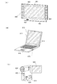
本実施の形態では、上記実施の形態で示した半導体装置を適用して作製した電子機器について、図13及び図14を参照しながら、説明する。
102 絶縁膜
104 脆化層
106 絶縁膜
107 レーザ光
108 ベース基板
109 微小ボイド
110 分離後のボンド基板
111a 分離面
111b 分離面
112 半導体膜
114 レーザ光
116 半導体膜
118 半導体膜
120 ゲート絶縁膜
122 第1の導電膜
124 第2の導電膜
125 積層導電膜
126 レジストマスク
128 レジストマスク
130 第1の導電膜
132 第1の導電膜
134 第2の導電膜
136 第2の導電膜
138 第2の導電膜
140 第2の導電膜
142 ゲート電極
144 ゲート電極
146 レジストマスク
148 p型不純物元素
150 高濃度不純物領域
152 低濃度不純物領域
154 チャネル形成領域
156 レジストマスク
158 n型不純物元素
160 高濃度不純物領域
162 低濃度不純物領域
164 チャネル形成領域
166 絶縁膜
168 第1の層間絶縁膜
170 第2の層間絶縁膜
172 配線
174 配線
200 第1の導電膜
202 第1の導電膜
204 第2の導電膜
206 第2の導電膜
208 ゲート電極
210 ゲート電極
212 低濃度不純物領域
214 チャネル形成領域
216 低濃度不純物領域
218 チャネル形成領域
220 サイドウォール
222 サイドウォール
224 高濃度不純物領域
226 低濃度不純物領域
228 チャネル形成領域
230 高濃度不純物領域
232 低濃度不純物領域
234 チャネル形成領域
302 単結晶半導体膜
320 単結晶半導体膜
322 走査線
323 信号線
324 画素電極
325 TFT
327 層間絶縁膜
328 電極
329 柱状スペーサ
330 配向膜
332 対向基板
333 対向電極
334 配向膜
335 液晶層
340 チャネル形成領域
341 高濃度不純物領域
401 選択用トランジスタ
402 表示制御用トランジスタ
403 半導体膜
404 半導体膜
405 走査線
406 信号線
407 電流供給線
408 画素電極
410 電極
411 電極
412 ゲート電極
413 電極
427 層間絶縁膜
428 隔壁層
429 EL層
430 対向電極
431 対向基板
432 樹脂層
451 チャネル形成領域
452 高濃度不純物領域
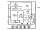
500 マイクロプロセッサ
501 演算回路
502 演算回路制御部
503 命令解析部
504 制御部
505 タイミング制御部
506 レジスタ
507 レジスタ制御部
508 バスインターフェース
509 専用メモリ
510 メモリインターフェース
511 RFCPU
512 アナログ回路部
513 デジタル回路部
514 共振回路
515 整流回路
516 定電圧回路
517 リセット回路
518 発振回路
519 復調回路
520 変調回路
521 RFインターフェース
522 制御レジスタ
523 クロックコントローラ
524 インターフェース
525 中央処理ユニット
526 ランダムアクセスメモリ
527 専用メモリ
528 アンテナ
529 容量部
530 電源管理回路
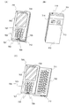
700 携帯電話
701 筐体
702 筐体
703 表示部
704 スピーカー
705 マイクロフォン
706 操作キー
707 ポインティングデバイス
708 表面カメラ用レンズ
709 外部接続端子ジャック
710 イヤホン端子
711 キーボード
712 外部メモリスロット
713 裏面カメラ
714 ライト
801 筐体
802 支持台
803 表示部
804 スピーカー部
805 ビデオ入力端子
812 筐体
813 表示部
814 キーボード
815 外部接続ポート
816 マウス
822 表示部
824 外部接続ポート
825 リモコン受信部
826 受像部
829 操作キー
1000 周辺部
1002 単結晶シリコン層
1004 熱酸化膜
1006 単結晶シリコン層
1008 熱酸化膜
1008 領域
1012 第1の領域
1014 第2の領域
1016 第3の領域
1018 第4の領域
1020 第5の領域
1022 第6の領域
Claims (15)
- ボンド基板上に絶縁膜を形成し、
前記絶縁膜を介して前記ボンド基板に水素イオンの照射を行うことにより、前記ボンド基板中に脆化層を形成し、
前記ボンド基板を、前記絶縁膜を介してベース基板と貼り合わせ、
熱処理によって前記ボンド基板を前記脆化層において分離し、
前記ベース基板上に前記絶縁膜を介して半導体膜を形成し、
前記半導体膜にレーザ光を照射し、
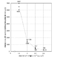
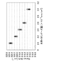
前記水素イオンの照射における水素イオンドーズ量は、前記熱処理により前記ボンド基板が分離する最小量となる水素イオンドーズ量の2.2倍以上とすることを特徴とするSOI基板の作製方法。 - 請求項1において、
前記水素イオンの照射における水素イオンドーズ量は、前記熱処理により前記ボンド基板が分離する最小量となる水素イオンドーズ量の2.2倍以上3.0倍以下とすることを特徴とするSOI基板の作製方法。 - ボンド基板上に絶縁膜を形成し、
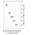
前記絶縁膜を介して前記ボンド基板に水素イオンの照射を行うことにより、前記ボンド基板中に脆化層を形成し、
前記ボンド基板を、前記絶縁膜を介してベース基板と貼り合わせ、
前記ボンド基板を前記脆化層において分離し、
前記ベース基板上に前記絶縁膜を介して半導体膜を形成し、
前記半導体膜にレーザ光を照射し、
前記水素イオンの照射における水素イオンドーズ量は、2.2×10¹⁶ions/cm2以上とすることを特徴とするSOI基板の作製方法。 - 請求項3において、
前記水素イオンの照射における水素イオンドーズ量は、2.2×10¹⁶ions/cm2以上3.0×1016ions/cm2以下とすることを特徴とするSOI基板の作製方法。 - 請求項1乃至請求項4のいずれか一項において、
前記レーザ光を照射する前に、前記半導体膜の表面に形成されている自然酸化膜を除去することを特徴とするSOI基板の作製方法。 - 請求項5において、
前記自然酸化膜を、ドライエッチングを用いて除去することを特徴とするSOI基板の作製方法。 - 請求項1乃至請求項6のいずれか一項において、
前記レーザ光の照射によって、前記半導体膜を部分溶融させることを特徴とするSOI基板の作製方法。 - 請求項1乃至請求項7のいずれか一項において、
前記絶縁膜は、酸化シリコン膜、窒化シリコン膜、酸化窒化シリコン膜若しくは窒化酸化シリコン膜から選ばれた単数の膜又は複数の膜の積層であることを特徴とするSOI基板の作製方法。 - 請求項1乃至請求項7のいずれか一項において、
前記絶縁膜は、前記酸化シリコン膜であり、有機シランガスを用いた化学気相成長法により形成されたものであることを特徴とするSOI基板の作製方法。 - 請求項1乃至請求項7のいずれか一項において、
前記絶縁膜は、前記酸化シリコン膜であり、前記ボンド基板を熱酸化して形成されたものであることを特徴とするSOI基板の作製方法。 - 請求項1乃至請求項10のいずれか一項において、
前記ベース基板上に接して第2の絶縁膜を形成することを特徴とするSOI基板の作製方法。 - 請求項11において、
前記第2の絶縁膜は、窒化シリコン膜又は窒化酸化シリコン膜であることを特徴とするSOI基板の作製方法。 - 請求項1乃至請求項12のいずれか一項において、
前記ボンド基板は、単結晶シリコン基板であることを特徴とするSOI基板の作製方法。 - 請求項1乃至請求項13のいずれか一項において、
前記ベース基板は、アルミノシリケートガラス、バリウムホウケイ酸ガラス、又はアルミノホウケイ酸ガラスであることを特徴とするSOI基板の作製方法。 - 請求項1乃至請求項14のいずれか一項において、
イオンドーピング装置を用いて前記水素イオンの照射を行うことを特徴とするSOI基板の作製方法。
Priority Applications (1)
| Application Number | Priority Date | Filing Date | Title |
|---|---|---|---|
| JP2009228249A JP2010109353A (ja) | 2008-10-02 | 2009-09-30 | Soi基板の作製方法 |
Applications Claiming Priority (2)
| Application Number | Priority Date | Filing Date | Title |
|---|---|---|---|
| JP2008257032 | 2008-10-02 | ||
| JP2009228249A JP2010109353A (ja) | 2008-10-02 | 2009-09-30 | Soi基板の作製方法 |
Publications (2)
| Publication Number | Publication Date |
|---|---|
| JP2010109353A true JP2010109353A (ja) | 2010-05-13 |
| JP2010109353A5 JP2010109353A5 (ja) | 2012-10-11 |
Family
ID=42076125
Family Applications (1)
| Application Number | Title | Priority Date | Filing Date |
|---|---|---|---|
| JP2009228249A Withdrawn JP2010109353A (ja) | 2008-10-02 | 2009-09-30 | Soi基板の作製方法 |
Country Status (2)
| Country | Link |
|---|---|
| US (1) | US8741740B2 (ja) |
| JP (1) | JP2010109353A (ja) |
Cited By (1)
| Publication number | Priority date | Publication date | Assignee | Title |
|---|---|---|---|---|
| KR20180100496A (ko) * | 2017-03-01 | 2018-09-11 | 가부시기가이샤 디스코 | 반도체 잉곳의 검사 방법, 검사 장치 및 레이저 가공 장치 |
Families Citing this family (9)
| Publication number | Priority date | Publication date | Assignee | Title |
|---|---|---|---|---|
| US8703521B2 (en) | 2009-06-09 | 2014-04-22 | International Business Machines Corporation | Multijunction photovoltaic cell fabrication |
| US8802477B2 (en) * | 2009-06-09 | 2014-08-12 | International Business Machines Corporation | Heterojunction III-V photovoltaic cell fabrication |
| KR101824537B1 (ko) * | 2010-10-01 | 2018-03-15 | 삼성디스플레이 주식회사 | 박막 트랜지스터 및 이를 포함하는 유기 발광 디스플레이 |
| US8766361B2 (en) * | 2010-12-16 | 2014-07-01 | Semiconductor Energy Laboratory Co., Ltd. | Semiconductor device and electronic device |
| US8318575B2 (en) * | 2011-02-07 | 2012-11-27 | Infineon Technologies Ag | Compressive polycrystalline silicon film and method of manufacture thereof |
| FR2978604B1 (fr) * | 2011-07-28 | 2018-09-14 | Soitec | Procede de guerison de defauts dans une couche semi-conductrice |
| JP5967211B2 (ja) * | 2013-04-04 | 2016-08-10 | 富士電機株式会社 | 半導体デバイスの製造方法 |
| KR20150012530A (ko) * | 2013-07-25 | 2015-02-04 | 삼성디스플레이 주식회사 | 전사용 도너 기판 및 유기 발광 표시 장치의 제조 방법 |
| CN107195689B (zh) * | 2017-07-21 | 2021-01-22 | 京东方科技集团股份有限公司 | 一种薄膜晶体管及其制作方法、oled显示面板 |
Citations (7)
| Publication number | Priority date | Publication date | Assignee | Title |
|---|---|---|---|---|
| JP2000077287A (ja) * | 1998-08-26 | 2000-03-14 | Nissin Electric Co Ltd | 結晶薄膜基板の製造方法 |
| JP2000294754A (ja) * | 1999-04-07 | 2000-10-20 | Denso Corp | 半導体基板及び半導体基板の製造方法並びに半導体基板製造装置 |
| JP2002305292A (ja) * | 2001-04-06 | 2002-10-18 | Shin Etsu Handotai Co Ltd | Soiウエーハおよびその製造方法 |
| JP2004063730A (ja) * | 2002-07-29 | 2004-02-26 | Shin Etsu Handotai Co Ltd | Soiウェーハの製造方法 |
| JP2004111521A (ja) * | 2002-09-17 | 2004-04-08 | Shin Etsu Handotai Co Ltd | Soiウエーハおよびその製造方法 |
| JP2004214400A (ja) * | 2002-12-27 | 2004-07-29 | Sumitomo Mitsubishi Silicon Corp | 半導体基板の製造方法 |
| JP2005203596A (ja) * | 2004-01-16 | 2005-07-28 | Seiko Epson Corp | 電気光学装置の製造方法、電気光学装置および電子機器 |
Family Cites Families (41)
| Publication number | Priority date | Publication date | Assignee | Title |
|---|---|---|---|---|
| FR2681472B1 (fr) * | 1991-09-18 | 1993-10-29 | Commissariat Energie Atomique | Procede de fabrication de films minces de materiau semiconducteur. |
| JP4103968B2 (ja) * | 1996-09-18 | 2008-06-18 | 株式会社半導体エネルギー研究所 | 絶縁ゲイト型半導体装置 |
| US6013563A (en) * | 1997-05-12 | 2000-01-11 | Silicon Genesis Corporation | Controlled cleaning process |
| US20070122997A1 (en) * | 1998-02-19 | 2007-05-31 | Silicon Genesis Corporation | Controlled process and resulting device |
| US6534380B1 (en) * | 1997-07-18 | 2003-03-18 | Denso Corporation | Semiconductor substrate and method of manufacturing the same |
| US6388652B1 (en) * | 1997-08-20 | 2002-05-14 | Semiconductor Energy Laboratory Co., Ltd. | Electrooptical device |
| US6686623B2 (en) * | 1997-11-18 | 2004-02-03 | Semiconductor Energy Laboratory Co., Ltd. | Nonvolatile memory and electronic apparatus |
| JP2000012864A (ja) * | 1998-06-22 | 2000-01-14 | Semiconductor Energy Lab Co Ltd | 半導体装置の作製方法 |
| JP3385972B2 (ja) * | 1998-07-10 | 2003-03-10 | 信越半導体株式会社 | 貼り合わせウェーハの製造方法および貼り合わせウェーハ |
| US6271101B1 (en) * | 1998-07-29 | 2001-08-07 | Semiconductor Energy Laboratory Co., Ltd. | Process for production of SOI substrate and process for production of semiconductor device |
| JP4476390B2 (ja) * | 1998-09-04 | 2010-06-09 | 株式会社半導体エネルギー研究所 | 半導体装置の作製方法 |
| JP2000124092A (ja) * | 1998-10-16 | 2000-04-28 | Shin Etsu Handotai Co Ltd | 水素イオン注入剥離法によってsoiウエーハを製造する方法およびこの方法で製造されたsoiウエーハ |
| KR20000040104A (ko) * | 1998-12-17 | 2000-07-05 | 김영환 | 실리콘 온 인슐레이터 웨이퍼의 제조방법 |
| EP1039513A3 (en) * | 1999-03-26 | 2008-11-26 | Canon Kabushiki Kaisha | Method of producing a SOI wafer |
| US7094667B1 (en) * | 2000-12-28 | 2006-08-22 | Bower Robert W | Smooth thin film layers produced by low temperature hydrogen ion cut |
| US7119365B2 (en) * | 2002-03-26 | 2006-10-10 | Sharp Kabushiki Kaisha | Semiconductor device and manufacturing method thereof, SOI substrate and display device using the same, and manufacturing method of the SOI substrate |
| JP4772258B2 (ja) | 2002-08-23 | 2011-09-14 | シャープ株式会社 | Soi基板の製造方法 |
| US6908797B2 (en) * | 2002-07-09 | 2005-06-21 | Semiconductor Energy Laboratory Co., Ltd. | Method of manufacturing a semiconductor device |
| US7508034B2 (en) * | 2002-09-25 | 2009-03-24 | Sharp Kabushiki Kaisha | Single-crystal silicon substrate, SOI substrate, semiconductor device, display device, and manufacturing method of semiconductor device |
| FR2847075B1 (fr) * | 2002-11-07 | 2005-02-18 | Commissariat Energie Atomique | Procede de formation d'une zone fragile dans un substrat par co-implantation |
| US7399681B2 (en) * | 2003-02-18 | 2008-07-15 | Corning Incorporated | Glass-based SOI structures |
| US7176528B2 (en) * | 2003-02-18 | 2007-02-13 | Corning Incorporated | Glass-based SOI structures |
| WO2005022610A1 (ja) * | 2003-09-01 | 2005-03-10 | Sumco Corporation | 貼り合わせウェーハの製造方法 |
| JP5110772B2 (ja) | 2004-02-03 | 2012-12-26 | 株式会社半導体エネルギー研究所 | 半導体薄膜層を有する基板の製造方法 |
| CN101091251B (zh) * | 2004-08-18 | 2011-03-16 | 康宁股份有限公司 | 包含高应变玻璃或玻璃陶瓷的绝缘体上半导体结构 |
| US7247545B2 (en) * | 2004-11-10 | 2007-07-24 | Sharp Laboratories Of America, Inc. | Fabrication of a low defect germanium film by direct wafer bonding |
| DE602004013163T2 (de) * | 2004-11-19 | 2009-05-14 | S.O.I. Tec Silicon On Insulator Technologies S.A. | Verfahren zur Herstellung eines Germanium-On-Insulator-Wafers (GeOI) |
| FR2888663B1 (fr) * | 2005-07-13 | 2008-04-18 | Soitec Silicon On Insulator | Procede de diminution de la rugosite d'une couche epaisse d'isolant |
| WO2007046290A1 (en) * | 2005-10-18 | 2007-04-26 | Semiconductor Energy Laboratory Co., Ltd. | Semiconductor device and manufacturing method thereof |
| US7419844B2 (en) * | 2006-03-17 | 2008-09-02 | Sharp Laboratories Of America, Inc. | Real-time CMOS imager having stacked photodiodes fabricated on SOI wafer |
| US7579654B2 (en) * | 2006-05-31 | 2009-08-25 | Corning Incorporated | Semiconductor on insulator structure made using radiation annealing |
| US7608521B2 (en) * | 2006-05-31 | 2009-10-27 | Corning Incorporated | Producing SOI structure using high-purity ion shower |
| FR2911430B1 (fr) * | 2007-01-15 | 2009-04-17 | Soitec Silicon On Insulator | "procede de fabrication d'un substrat hybride" |
| CN101281912B (zh) * | 2007-04-03 | 2013-01-23 | 株式会社半导体能源研究所 | Soi衬底及其制造方法以及半导体装置 |
| KR101447048B1 (ko) * | 2007-04-20 | 2014-10-06 | 가부시키가이샤 한도오따이 에네루기 켄큐쇼 | Soi 기판 및 반도체장치의 제조방법 |
| KR101440930B1 (ko) * | 2007-04-20 | 2014-09-15 | 가부시키가이샤 한도오따이 에네루기 켄큐쇼 | Soi 기판의 제작방법 |
| EP1986230A2 (en) * | 2007-04-25 | 2008-10-29 | Semiconductor Energy Laboratory Co., Ltd. | Method of manufacturing SOI substrate and method of manufacturing semiconductor device |
| EP1993128A3 (en) * | 2007-05-17 | 2010-03-24 | Semiconductor Energy Laboratory Co., Ltd. | Method for manufacturing soi substrate |
| EP1993127B1 (en) * | 2007-05-18 | 2013-04-24 | Semiconductor Energy Laboratory Co., Ltd. | Manufacturing method of SOI substrate |
| KR101484296B1 (ko) * | 2007-06-26 | 2015-01-19 | 가부시키가이샤 한도오따이 에네루기 켄큐쇼 | 반도체 기판의 제작방법 |
| WO2009151513A1 (en) * | 2008-05-01 | 2009-12-17 | Corning Incorporated | Raised features on transparent substrates and related methods |
-
2009
- 2009-09-29 US US12/568,772 patent/US8741740B2/en not_active Expired - Fee Related
- 2009-09-30 JP JP2009228249A patent/JP2010109353A/ja not_active Withdrawn
Patent Citations (7)
| Publication number | Priority date | Publication date | Assignee | Title |
|---|---|---|---|---|
| JP2000077287A (ja) * | 1998-08-26 | 2000-03-14 | Nissin Electric Co Ltd | 結晶薄膜基板の製造方法 |
| JP2000294754A (ja) * | 1999-04-07 | 2000-10-20 | Denso Corp | 半導体基板及び半導体基板の製造方法並びに半導体基板製造装置 |
| JP2002305292A (ja) * | 2001-04-06 | 2002-10-18 | Shin Etsu Handotai Co Ltd | Soiウエーハおよびその製造方法 |
| JP2004063730A (ja) * | 2002-07-29 | 2004-02-26 | Shin Etsu Handotai Co Ltd | Soiウェーハの製造方法 |
| JP2004111521A (ja) * | 2002-09-17 | 2004-04-08 | Shin Etsu Handotai Co Ltd | Soiウエーハおよびその製造方法 |
| JP2004214400A (ja) * | 2002-12-27 | 2004-07-29 | Sumitomo Mitsubishi Silicon Corp | 半導体基板の製造方法 |
| JP2005203596A (ja) * | 2004-01-16 | 2005-07-28 | Seiko Epson Corp | 電気光学装置の製造方法、電気光学装置および電子機器 |
Cited By (2)
| Publication number | Priority date | Publication date | Assignee | Title |
|---|---|---|---|---|
| KR20180100496A (ko) * | 2017-03-01 | 2018-09-11 | 가부시기가이샤 디스코 | 반도체 잉곳의 검사 방법, 검사 장치 및 레이저 가공 장치 |
| KR102298614B1 (ko) | 2017-03-01 | 2021-09-03 | 가부시기가이샤 디스코 | 반도체 잉곳의 검사 방법, 검사 장치 및 레이저 가공 장치 |
Also Published As
| Publication number | Publication date |
|---|---|
| US8741740B2 (en) | 2014-06-03 |
| US20100087045A1 (en) | 2010-04-08 |
Similar Documents
| Publication | Publication Date | Title |
|---|---|---|
| TWI538111B (zh) | Soi基板的製造方法 | |
| US8313989B2 (en) | SOI substrate and method for manufacturing the same | |
| US8741740B2 (en) | Method for manufacturing SOI substrate | |
| JP5568260B2 (ja) | Soi基板の作製方法 | |
| TWI494974B (zh) | Soi基板的製造方法 | |
| JP5478166B2 (ja) | 半導体装置の作製方法 | |
| JP5663150B2 (ja) | Soi基板の作製方法 | |
| JP2010034535A (ja) | Soi基板の作製方法 | |
| KR20100038165A (ko) | Soi 기판의 제작 방법 | |
| JP2009212503A (ja) | Soi基板の作製方法 | |
| JP2009260315A (ja) | Soi基板の作製方法及び半導体装置の作製方法 | |
| JP5666794B2 (ja) | Soi基板の作製方法 | |
| JP2010114431A (ja) | Soi基板の作製方法 | |
| JP2009260313A (ja) | Soi基板の作製方法及び半導体装置の作製方法 | |
| JP5667767B2 (ja) | Soi基板の作製方法 | |
| US20100173472A1 (en) | Method for manufacturing soi substrate and method for manufacturing semiconductor device | |
| JP5618521B2 (ja) | 半導体装置の作製方法 | |
| JP2010087485A (ja) | Soi基板の作製方法 | |
| JP5438945B2 (ja) | ボンド基板の作製方法 |
Legal Events
| Date | Code | Title | Description |
|---|---|---|---|
| A521 | Written amendment |
Free format text: JAPANESE INTERMEDIATE CODE: A523 Effective date: 20120823 |
|
| A621 | Written request for application examination |
Free format text: JAPANESE INTERMEDIATE CODE: A621 Effective date: 20120823 |
|
| A977 | Report on retrieval |
Free format text: JAPANESE INTERMEDIATE CODE: A971007 Effective date: 20131226 |
|
| A131 | Notification of reasons for refusal |
Free format text: JAPANESE INTERMEDIATE CODE: A131 Effective date: 20140107 |
|
| A521 | Written amendment |
Free format text: JAPANESE INTERMEDIATE CODE: A523 Effective date: 20140210 |
|
| A02 | Decision of refusal |
Free format text: JAPANESE INTERMEDIATE CODE: A02 Effective date: 20140624 |
|
| A761 | Written withdrawal of application |
Free format text: JAPANESE INTERMEDIATE CODE: A761 Effective date: 20140901 |