JP2010067852A - 回路装置の製造方法 - Google Patents
回路装置の製造方法 Download PDFInfo
- Publication number
- JP2010067852A JP2010067852A JP2008233781A JP2008233781A JP2010067852A JP 2010067852 A JP2010067852 A JP 2010067852A JP 2008233781 A JP2008233781 A JP 2008233781A JP 2008233781 A JP2008233781 A JP 2008233781A JP 2010067852 A JP2010067852 A JP 2010067852A
- Authority
- JP
- Japan
- Prior art keywords
- circuit board
- resin
- mold
- sealing resin
- resin sheet
- Prior art date
- Legal status (The legal status is an assumption and is not a legal conclusion. Google has not performed a legal analysis and makes no representation as to the accuracy of the status listed.)
- Granted
Links
Images


Classifications
-
- H10W72/381—
-
- H10W72/884—
-
- H10W74/00—
Landscapes
- Encapsulation Of And Coatings For Semiconductor Or Solid State Devices (AREA)
Abstract
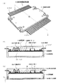
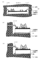
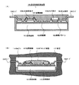
【解決手段】本発明では、半導体素子等の回路素子が組み込まれた回路基板12を金型30の内部に収納させ、熱硬化性樹脂を含む樹脂シート42を、回路基板12と金型30の内壁下面との間に介在させている。この状態で、金型30を180℃程度に加熱し、ゲート44から液状の封止樹脂を注入することで、溶融した樹脂シート42により回路基板12の下面を薄く封止樹脂により被覆することができる。
【選択図】図2
Description
12 回路基板
14 封止樹脂
14A 第1封止樹脂
14B 第2封止樹脂
16 導電パターン
17 リード
18 絶縁層
20A 半導体素子
20B チップ素子
22 金属細線
30 金型
32 上金型
34 下金型
36 キャビティ
38 ランナー
40,40A,40B,40C ポッド
42 樹脂シート
44 ゲート
46 エアベント
48 タブレット
50 プランジャー
52 当接ピン
Claims (7)
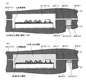
- 導電パターンおよび回路素子から成る混成集積回路を回路基板の上面に組み込む工程と、
前記回路基板をモールド金型のキャビティに収納させて、前記キャビティに封止樹脂を注入することで、前記回路基板の上面、側面および下面を、熱硬化性樹脂を含む封止樹脂により封止する工程と、を備え、
前記封止する工程では、熱硬化性樹脂を含む樹脂シートを、前記回路基板と前記モールド金型の内壁下面との間に介在させ、溶融した前記樹脂シートにより前記回路基板の下面を被覆することを特徴とする回路装置の製造方法。 - 前記封止する工程では、
前記回路基板の対向する側辺から導出されるリードを前記モールド金型で狭持することにより、前記樹脂シートが前記回路基板の下面に押圧された状態で固定され、
溶融した前記樹脂シートから成る封止樹脂により前記回路基板の下面が被覆される厚さは、前記樹脂シートよりも薄いことを特徴とする請求項1記載の回路装置の製造方法。 - 前記封止する工程では、前記樹脂シートを溶融させた後に、前記モールド金型のゲートから前記キャビティに液状の封止樹脂を注入し、
前記樹脂シートを、前記注入される前記封止樹脂よりも先に加熱硬化させることを特徴とする請求項2記載の回路装置の製造方法。 - 前記樹脂シートは、加熱硬化する前の粉体の前記熱硬化性樹脂を加圧して成形されることを特徴とする請求項3記載の回路装置の製造方法。
- 前記モールド金型のゲートから前記キャビティに注入される樹脂と、前記樹脂シートとは組成が同じであることを特徴とする請求項4記載の回路装置の製造方法。
- 前記樹脂シートの大きさを前記回路基板よりも大きく形成し、前記回路基板の下面全域を前記樹脂シートにより被覆することを特徴とする請求項5記載の回路装置の製造方法。
- 溶融した前記樹脂シートから成り前記回路基板の下面を被覆する前記封止樹脂に含まれるフィラーは、前記ゲートから注入されて前記回路基板の上面を被覆する前記封止樹脂に含まれるフィラーよりも、均一に分散した状態であることを特徴とする請求項6記載の回路装置の製造方法。
Priority Applications (2)
| Application Number | Priority Date | Filing Date | Title |
|---|---|---|---|
| JP2008233781A JP5308108B2 (ja) | 2008-09-11 | 2008-09-11 | 回路装置の製造方法 |
| US12/557,882 US8084301B2 (en) | 2008-09-11 | 2009-09-11 | Resin sheet, circuit device and method of manufacturing the same |
Applications Claiming Priority (1)
| Application Number | Priority Date | Filing Date | Title |
|---|---|---|---|
| JP2008233781A JP5308108B2 (ja) | 2008-09-11 | 2008-09-11 | 回路装置の製造方法 |
Publications (2)
| Publication Number | Publication Date |
|---|---|
| JP2010067852A true JP2010067852A (ja) | 2010-03-25 |
| JP5308108B2 JP5308108B2 (ja) | 2013-10-09 |
Family
ID=42193172
Family Applications (1)
| Application Number | Title | Priority Date | Filing Date |
|---|---|---|---|
| JP2008233781A Active JP5308108B2 (ja) | 2008-09-11 | 2008-09-11 | 回路装置の製造方法 |
Country Status (1)
| Country | Link |
|---|---|
| JP (1) | JP5308108B2 (ja) |
Cited By (5)
| Publication number | Priority date | Publication date | Assignee | Title |
|---|---|---|---|---|
| JP2012004435A (ja) * | 2010-06-18 | 2012-01-05 | On Semiconductor Trading Ltd | 回路装置の製造方法および樹脂封止装置 |
| KR20130138010A (ko) * | 2012-06-08 | 2013-12-18 | 현대모비스 주식회사 | 휴대용 전자통신 장치 및 이의 제조 방법 |
| US8614397B2 (en) | 2010-07-22 | 2013-12-24 | On Semiconductor Trading, Ltd. | Circuit device |
| US8624408B2 (en) | 2010-07-22 | 2014-01-07 | On Semiconductor Trading, Ltd. | Circuit device and method of manufacturing the same |
| CN117334644A (zh) * | 2023-11-29 | 2024-01-02 | 四川弘智远大科技有限公司 | 一种集成电路封装的实时固化结构 |
Citations (5)
| Publication number | Priority date | Publication date | Assignee | Title |
|---|---|---|---|---|
| JPH05102216A (ja) * | 1991-10-09 | 1993-04-23 | Hitachi Ltd | 半導体装置 |
| JPH05198707A (ja) * | 1992-01-22 | 1993-08-06 | Nec Kyushu Ltd | 半導体装置の製造方法 |
| JPH05243301A (ja) * | 1992-02-28 | 1993-09-21 | Nec Kyushu Ltd | 半導体装置製造方法 |
| JP2000114295A (ja) * | 1998-09-30 | 2000-04-21 | Mitsui High Tec Inc | 半導体装置の製造方法 |
| JP2003017631A (ja) * | 2001-06-28 | 2003-01-17 | Sanyo Electric Co Ltd | 混成集積回路装置およびその製造方法 |
-
2008
- 2008-09-11 JP JP2008233781A patent/JP5308108B2/ja active Active
Patent Citations (5)
| Publication number | Priority date | Publication date | Assignee | Title |
|---|---|---|---|---|
| JPH05102216A (ja) * | 1991-10-09 | 1993-04-23 | Hitachi Ltd | 半導体装置 |
| JPH05198707A (ja) * | 1992-01-22 | 1993-08-06 | Nec Kyushu Ltd | 半導体装置の製造方法 |
| JPH05243301A (ja) * | 1992-02-28 | 1993-09-21 | Nec Kyushu Ltd | 半導体装置製造方法 |
| JP2000114295A (ja) * | 1998-09-30 | 2000-04-21 | Mitsui High Tec Inc | 半導体装置の製造方法 |
| JP2003017631A (ja) * | 2001-06-28 | 2003-01-17 | Sanyo Electric Co Ltd | 混成集積回路装置およびその製造方法 |
Cited By (6)
| Publication number | Priority date | Publication date | Assignee | Title |
|---|---|---|---|---|
| JP2012004435A (ja) * | 2010-06-18 | 2012-01-05 | On Semiconductor Trading Ltd | 回路装置の製造方法および樹脂封止装置 |
| US8614397B2 (en) | 2010-07-22 | 2013-12-24 | On Semiconductor Trading, Ltd. | Circuit device |
| US8624408B2 (en) | 2010-07-22 | 2014-01-07 | On Semiconductor Trading, Ltd. | Circuit device and method of manufacturing the same |
| KR20130138010A (ko) * | 2012-06-08 | 2013-12-18 | 현대모비스 주식회사 | 휴대용 전자통신 장치 및 이의 제조 방법 |
| CN117334644A (zh) * | 2023-11-29 | 2024-01-02 | 四川弘智远大科技有限公司 | 一种集成电路封装的实时固化结构 |
| CN117334644B (zh) * | 2023-11-29 | 2024-02-13 | 四川弘智远大科技有限公司 | 一种集成电路封装的实时固化结构 |
Also Published As
| Publication number | Publication date |
|---|---|
| JP5308108B2 (ja) | 2013-10-09 |
Similar Documents
| Publication | Publication Date | Title |
|---|---|---|
| TWI260036B (en) | Semiconductor device, method of manufacturing semiconductor device, resin molding die, and semiconductor manufacturing system | |
| KR101316289B1 (ko) | 회로 장치 및 그 제조 방법 | |
| US8084301B2 (en) | Resin sheet, circuit device and method of manufacturing the same | |
| CN102347245B (zh) | 电路装置的制造方法 | |
| CN105643855B (zh) | 电子部件、其制造方法及制造装置 | |
| CN102005419A (zh) | 功率用半导体装置及其制造方法 | |
| JP5308108B2 (ja) | 回路装置の製造方法 | |
| JP5542318B2 (ja) | 樹脂シートおよびそれを用いた回路装置の製造方法 | |
| CN111863742B (zh) | 半导体装置 | |
| JP5308107B2 (ja) | 回路装置の製造方法 | |
| JP2011114134A (ja) | 回路装置の製造方法 | |
| WO2013061603A1 (ja) | 回路装置の製造方法 | |
| KR101316273B1 (ko) | 회로 장치 | |
| JP2006086337A (ja) | 樹脂封止型電子装置及びその製法 | |
| JP2010086996A (ja) | 回路装置の製造方法 | |
| JP2013115133A (ja) | 回路装置の製造方法 | |
| JP2013105759A (ja) | 回路装置 | |
| JP2013105758A (ja) | 回路装置およびその製造方法 | |
| JP2013120914A (ja) | 回路装置の製造方法 | |
| JP2010086991A (ja) | 回路装置およびその製造方法 | |
| JP2002083833A (ja) | 半導体装置及びその製造方法 |
Legal Events
| Date | Code | Title | Description |
|---|---|---|---|
| A711 | Notification of change in applicant |
Free format text: JAPANESE INTERMEDIATE CODE: A711 Effective date: 20110609 |
|
| A621 | Written request for application examination |
Free format text: JAPANESE INTERMEDIATE CODE: A621 Effective date: 20110905 |
|
| A977 | Report on retrieval |
Free format text: JAPANESE INTERMEDIATE CODE: A971007 Effective date: 20120725 |
|
| A131 | Notification of reasons for refusal |
Free format text: JAPANESE INTERMEDIATE CODE: A131 Effective date: 20120731 |
|
| A521 | Request for written amendment filed |
Free format text: JAPANESE INTERMEDIATE CODE: A523 Effective date: 20121023 |
|
| A131 | Notification of reasons for refusal |
Free format text: JAPANESE INTERMEDIATE CODE: A131 Effective date: 20121128 |
|
| A521 | Request for written amendment filed |
Free format text: JAPANESE INTERMEDIATE CODE: A523 Effective date: 20130213 |
|
| A711 | Notification of change in applicant |
Free format text: JAPANESE INTERMEDIATE CODE: A711 Effective date: 20130215 |
|
| A521 | Request for written amendment filed |
Free format text: JAPANESE INTERMEDIATE CODE: A523 Effective date: 20130405 |
|
| TRDD | Decision of grant or rejection written | ||
| A01 | Written decision to grant a patent or to grant a registration (utility model) |
Free format text: JAPANESE INTERMEDIATE CODE: A01 Effective date: 20130604 |
|
| A61 | First payment of annual fees (during grant procedure) |
Free format text: JAPANESE INTERMEDIATE CODE: A61 Effective date: 20130628 |
|
| R150 | Certificate of patent or registration of utility model |
Ref document number: 5308108 Country of ref document: JP Free format text: JAPANESE INTERMEDIATE CODE: R150 |
|
| RD04 | Notification of resignation of power of attorney |
Free format text: JAPANESE INTERMEDIATE CODE: R3D04 |
|
| R250 | Receipt of annual fees |
Free format text: JAPANESE INTERMEDIATE CODE: R250 |
|
| R250 | Receipt of annual fees |
Free format text: JAPANESE INTERMEDIATE CODE: R250 |
|
| R250 | Receipt of annual fees |
Free format text: JAPANESE INTERMEDIATE CODE: R250 |
|
| R250 | Receipt of annual fees |
Free format text: JAPANESE INTERMEDIATE CODE: R250 |
|
| R250 | Receipt of annual fees |
Free format text: JAPANESE INTERMEDIATE CODE: R250 |
|
| R250 | Receipt of annual fees |
Free format text: JAPANESE INTERMEDIATE CODE: R250 |
|
| R250 | Receipt of annual fees |
Free format text: JAPANESE INTERMEDIATE CODE: R250 |
|
| R250 | Receipt of annual fees |
Free format text: JAPANESE INTERMEDIATE CODE: R250 |
|
| R250 | Receipt of annual fees |
Free format text: JAPANESE INTERMEDIATE CODE: R250 |
|
| R250 | Receipt of annual fees |
Free format text: JAPANESE INTERMEDIATE CODE: R250 |