JP2010054943A - スポットサイズ変換器 - Google Patents
スポットサイズ変換器 Download PDFInfo
- Publication number
- JP2010054943A JP2010054943A JP2008221515A JP2008221515A JP2010054943A JP 2010054943 A JP2010054943 A JP 2010054943A JP 2008221515 A JP2008221515 A JP 2008221515A JP 2008221515 A JP2008221515 A JP 2008221515A JP 2010054943 A JP2010054943 A JP 2010054943A
- Authority
- JP
- Japan
- Prior art keywords
- core
- region
- spot size
- size converter
- clad
- Prior art date
- Legal status (The legal status is an assumption and is not a legal conclusion. Google has not performed a legal analysis and makes no representation as to the accuracy of the status listed.)
- Granted
Links
- 239000000758 substrate Substances 0.000 claims abstract description 33
- 238000005253 cladding Methods 0.000 claims description 38
- 238000004519 manufacturing process Methods 0.000 claims description 36
- 238000005530 etching Methods 0.000 claims description 31
- 230000003287 optical effect Effects 0.000 claims description 25
- 239000002243 precursor Substances 0.000 claims description 23
- 229910004298 SiO 2 Inorganic materials 0.000 claims description 9
- 230000010287 polarization Effects 0.000 abstract description 8
- 230000001902 propagating effect Effects 0.000 abstract description 7
- 238000005520 cutting process Methods 0.000 abstract description 2
- 238000000034 method Methods 0.000 description 26
- 239000011347 resin Substances 0.000 description 21
- 229920005989 resin Polymers 0.000 description 21
- 238000004088 simulation Methods 0.000 description 19
- 230000008878 coupling Effects 0.000 description 11
- 238000010168 coupling process Methods 0.000 description 11
- 238000005859 coupling reaction Methods 0.000 description 11
- 239000000284 extract Substances 0.000 description 7
- 229920002120 photoresistant polymer Polymers 0.000 description 7
- 230000007423 decrease Effects 0.000 description 6
- 239000000463 material Substances 0.000 description 6
- 230000002093 peripheral effect Effects 0.000 description 6
- 229910021421 monocrystalline silicon Inorganic materials 0.000 description 5
- 239000013307 optical fiber Substances 0.000 description 5
- 238000013459 approach Methods 0.000 description 4
- 230000000694 effects Effects 0.000 description 4
- 238000001020 plasma etching Methods 0.000 description 4
- 229920001721 polyimide Polymers 0.000 description 4
- 239000004642 Polyimide Substances 0.000 description 2
- 238000004364 calculation method Methods 0.000 description 2
- 238000010276 construction Methods 0.000 description 2
- 238000000151 deposition Methods 0.000 description 2
- 238000000206 photolithography Methods 0.000 description 2
- 239000009719 polyimide resin Substances 0.000 description 2
- 239000004065 semiconductor Substances 0.000 description 2
- 229910052710 silicon Inorganic materials 0.000 description 2
- 239000004925 Acrylic resin Substances 0.000 description 1
- 229920000178 Acrylic resin Polymers 0.000 description 1
- 108010015780 Viral Core Proteins Proteins 0.000 description 1
- 238000005452 bending Methods 0.000 description 1
- 230000015572 biosynthetic process Effects 0.000 description 1
- 238000006243 chemical reaction Methods 0.000 description 1
- 238000005229 chemical vapour deposition Methods 0.000 description 1
- 238000007796 conventional method Methods 0.000 description 1
- 230000001419 dependent effect Effects 0.000 description 1
- 230000008021 deposition Effects 0.000 description 1
- 238000011161 development Methods 0.000 description 1
- 238000005516 engineering process Methods 0.000 description 1
- 239000003822 epoxy resin Substances 0.000 description 1
- 239000011521 glass Substances 0.000 description 1
- 239000012212 insulator Substances 0.000 description 1
- 230000003647 oxidation Effects 0.000 description 1
- 238000007254 oxidation reaction Methods 0.000 description 1
- 229920000647 polyepoxide Polymers 0.000 description 1
- 238000002360 preparation method Methods 0.000 description 1
- 239000010703 silicon Substances 0.000 description 1
- 238000012546 transfer Methods 0.000 description 1
Images


Classifications
-
- G—PHYSICS
- G02—OPTICS
- G02B—OPTICAL ELEMENTS, SYSTEMS OR APPARATUS
- G02B6/00—Light guides; Structural details of arrangements comprising light guides and other optical elements, e.g. couplings
- G02B6/10—Light guides; Structural details of arrangements comprising light guides and other optical elements, e.g. couplings of the optical waveguide type
- G02B6/12—Light guides; Structural details of arrangements comprising light guides and other optical elements, e.g. couplings of the optical waveguide type of the integrated circuit kind
- G02B6/122—Basic optical elements, e.g. light-guiding paths
- G02B6/1228—Tapered waveguides, e.g. integrated spot-size transformers
Landscapes
- Engineering & Computer Science (AREA)
- Physics & Mathematics (AREA)
- Power Engineering (AREA)
- Microelectronics & Electronic Packaging (AREA)
- General Physics & Mathematics (AREA)
- Optics & Photonics (AREA)
- Optical Integrated Circuits (AREA)
Abstract
【解決手段】基板12の第1主面12aに配置されるクラッド14と、クラッド内に設けられていて、クラッドから露出した傾斜面18aを有する光入出力領域16を備えていて直線状に延在し、第1側面と、第1側面に平行に対向する第2側面182と、第1及び第2側面の双方に垂直であって互いに対向する第3側面及び第4側面184で囲まれることにより、光伝播方向に垂直な横断面形状が矩形状の第1コア18と、光入出力領域の傾斜面18aを包含するようにクラッド上に配置される第2コア20とを備えていて、光入出力領域は、第3及び第4側面の双方に対して垂直な平面であって、第1側面から第2側面に至るまでの間を斜めに切断した傾斜面が延在する領域であることを特徴とする。
【選択図】図1−C
Description
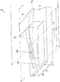
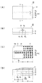
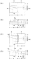
図1〜図5を参照して、実施の形態1のスポットサイズ変換器及びその製造方法について説明する。図1−Aは、スポットサイズ変換器の要部の部分的な構造を概略的に示す斜視図である。図1−Bは、図1−AのI−I線に沿って取った断面図である。図1−Cは、スポットサイズ変換器の要部の全体像を概略的に示す斜視図である。図2(A)は、図1−CのC−C線に沿って取った切断端面図である。図2(B)は図1−CのD−D線に沿って取った切断端面図である。
図1を参照すると、スポットサイズ変換器10は、クラッド14と、光入出領域16及び主要コア領域17を備えた第1コア18と、第2コア20とを備えている。
(2)n1>n3>n2
つまり、第1コア18の屈折率n1を、クラッド14の屈折率n2よりも40%以上大きな値とし、及び、第2コア20の屈折率n3を、クラッド14の屈折率n2を超え、かつ第1コア18の屈折率n1未満の値とする。
次に、図1及び図2を参照して、スポットサイズ変換器10の動作について説明する。なお、以下の説明は、スポットサイズ変換器10から外部の光学装置(例えば、光ファイバやLD)へと光を結合する場合の例であるが、逆に、外部の光学装置からスポットサイズ変換器10へと光を結合する場合にも同様に適用可能である。
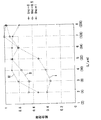
続いて、主に図2及び図3を参照して、スポットサイズ変換器10のシミュレーション結果について説明する。図3は、シミュレーションの説明に供するグラフである。
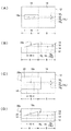
次に、図4〜図5を参照して、スポットサイズ変換器10の製造方法について説明する。なお、図4(A)は、スポットサイズ変換器10の製造工程の一部工程段階を抜き出して示す平面図である。図4(B)は、図4(A)のC−C線に沿った切断端面図である。図4(C)は、スポットサイズ変換器10の製造工程の一部工程段階を抜き出して示す平面図である。図4(D)は、図4(C)の側面図である。図5(A)は、スポットサイズ変換器10の製造工程の一部工程段階を抜き出して示す平面図である。図5(B)は、図5(A)の側面図である。図5(C)は、スポットサイズ変換器10の製造工程の一部工程段階を抜き出して示す平面図である。図5(D)は、図5(C)の側面図である。
まず、基板12の第1主面12aに配置されたクラッド14中に第1コア18が埋め込まれた前駆体22を準備する。
続いて、前駆体22の露出したクラッド14の表面14aにおいて、第1コア18の第1及び第2側面181及び182に対応する領域に、第1コア18の延在方向に沿って、予め定められた厚みから徐々に厚みが0にまで変化するエッチングマスクを設ける第1工程を行う。
続いて、エッチングマスク(感光性樹脂R)をマスクとして、前駆体22の露出した表面から第1コア18の下側に延在するクラッド14に至るまで異方性エッチングを行うことにより、第3及び第4側面183及び184の双方に対して垂直な平面であって、第1側面181から第2側面182に至るまでの間を斜めに切断した傾斜面18aが延在する領域としての光入出力領域16を形成する。
続いて、クラッド14と第1コア18との接触領域を除いた光入出力領域16を埋め込むように、クラッド14上に前記第2コア20を形成する。
以下、この実施の形態のスポットサイズ変換器10及びその製造方法の奏する効果について説明する。
続いて、図6〜図10を参照して実施の形態2のスポットサイズ変換器30及びその製造方法について説明する。図6は、スポットサイズ変換器30の概略的な構造を示す斜視図である。図7は、図6のC−C線に沿って取った切断端面図である。
図6を参照すると明らかなように、この実施の形態のスポットサイズ変換器30は、実施の形態1のスポットサイズ変換器10と、光入出力領域16の構造が異なっている以外は、同様に構成されている。従って、以下の説明においては、図1と同様の構成要素には同符号を付し、その説明を省略するとともに、実施の形態1のスポットサイズ変換器10との相違点を中心に説明する。
続いて、主に、図7及び図8を参照して、スポットサイズ変換器30のシミュレーション結果について説明する。図8は、シミュレーションの説明に供するグラフである。
次に、図4及び図9〜図10を参照して、スポットサイズ変換器30の製造方法について説明する。図9(A)は、スポットサイズ変換器30の製造工程の一部工程段階を抜き出して示す平面図である。図9(B)は、図9(A)の側面図である。図10(A)は、スポットサイズ変換器30の製造工程の一部工程段階を抜き出して示す平面図である。図10(B)は、図10(A)の側面図である。図10(C)は、スポットサイズ変換器30の製造工程の一部工程段階を抜き出して示す平面図である。図10(D)は、図10(C)の側面図である。
この準備工程は、実施の形態1の準備工程と同様にすることにより、図4(A)及び(B)に示すような前駆体22を得る。
続いて、図9(A)及び(B)に示すように、前駆体22の露出したクラッド14の表面において、第1コア34の第3及び第4側面343及び344に対応する領域を斜めに横切るようにエッチングマスクを設ける第1工程を行う。
続いて、図10(A)及び(B)に示すように、エッチングマスク(フォトレジストP)をマスクとして、前駆体22の露出した表面から第1コア34の下側に延在するクラッド14に至るまで異方性エッチングを行うことにより、第3及び第4側面343及び344の双方に対して垂直な平面であって、第1側面341から第2側面342に至るまでの間を斜めに切断した傾斜面34aが延在する領域としての光入出力領域16を形成する第2工程を行う。
この第3工程は、実施の形態1の第3工程と同様にすることにより、図10(C)及び(D)に示すようなスポットサイズ変換器30を得る。
以下、この実施の形態のスポットサイズ変換器30及びその製造方法の奏する効果について説明する。
12 基板
12a 第1主面
14 クラッド
14a 表面
16 光入出力領域
17 主要コア領域
18,34 第1コア
181,341 第1側面
182,342 第2側面
183,343 第3側面
184,344 第4側面
18a,34a 傾斜面
19 突出部
20 第2コア
20a 光入出射端面
22 前駆体
Claims (6)
- 基板の第1主面に配置されるクラッドと、
(a)該クラッド内に直線状に延在して設けられていて、第1側面と、該第1側面に平行に対向する第2側面と、該第1及び第2側面の双方に垂直であって互いに対向する第3及び第4側面とを有する直方体形状の主要コア領域、及び
(b)該主要コア領域の一端面から一体的に延在し、かつ前記クラッドから露出して設けられた光入出力領域とを有する第1コアと、
前記光入出力領域の前記傾斜面を包含するように前記クラッド上に配置される第2コアとを備えていて、
前記第1コアの屈折率を、前記クラッドの屈折率よりも40%以上大きな値とし、
前記第2コアの屈折率を、前記クラッドの屈折率を超え、かつ前記第1コアの屈折率未満の値とし、
前記光入出力領域は、前記第3及び第4側面の双方に対して垂直な平面であって、前記第1側面から前記第2側面に至るまでの間を斜めに延在する傾斜面を有することを特徴とするスポットサイズ変換器。 - 前記第1及び第2側面が、前記基板の前記第1主面に平行に延在していることを特徴とする請求項1に記載のスポットサイズ変換器。
- 前記第1及び第2側面が、前記基板の前記第1主面に垂直に延在していることを特徴とする請求項1に記載のスポットサイズ変換器。
- 前記クラッドをSiO2とし、及び前記第1コアをSiとすることを特徴とする請求項1〜3のいずれか一項に記載のスポットサイズ変換器。
- 請求項2に記載のスポットサイズ変換器の製造方法であって、
前記基板の前記第1主面に配置された前記クラッド中に前記第1コアが埋め込まれた前駆体を準備し、
当該前駆体の露出したクラッドの表面に、形成されるべき前記光入出力領域の前記傾斜面の直上領域における厚みが、前記第1コアの延在方向に沿って、予め定められた厚みから線形的に厚みが0にまで変化するエッチングマスクを設ける第1工程と、
該エッチングマスクをマスクとして、前記前駆体の露出した前記表面から前記第1コアの下側に延在するクラッドに至るまで異方性エッチングを行うことにより、前記第3及び第4側面の双方に対して垂直な平面であって、前記第1側面から前記第2側面に至るまでの間を斜めに切断した傾斜面が延在する領域としての前記光入出力領域を形成する第2工程と、
前記クラッドと前記第1コアとの接触領域を除いた光入出力領域を埋め込むように、該クラッド上に前記第2コアを形成する第3工程とを含むことを特徴とするスポットサイズ変換器の製造方法。 - 請求項3に記載のスポットサイズ変換器の製造方法であって、
前記基板の前記第1主面に配置された前記クラッド中に前記第1コアが埋め込まれた前駆体を準備し、
当該前駆体の露出したクラッドの表面において、前記第1コアの前記第3及び第4側面に対応する領域を斜めに横切るようにエッチングマスクを設ける第1工程と、
当該エッチングマスクをマスクとして、前記前駆体の露出した前記表面から前記第1コアの下側に延在するクラッドに至るまで異方性エッチングを行うことにより、前記第3及び第4側面の双方に対して垂直な平面であって、前記第1側面から前記第2側面に至るまでの間を斜めに切断した切断面が延在する領域としての前記光入出力領域を形成する第2工程と、
前記クラッドと第1コアとの接触領域を除いた前記光入出力領域を埋め込むように、該クラッド上に前記第2コアを形成する第3工程とを含むことを特徴とするスポットサイズ変換器の製造方法。
Priority Applications (2)
| Application Number | Priority Date | Filing Date | Title |
|---|---|---|---|
| JP2008221515A JP5104665B2 (ja) | 2008-08-29 | 2008-08-29 | スポットサイズ変換器 |
| US12/453,366 US7664352B1 (en) | 2008-08-29 | 2009-05-08 | Spot size converter |
Applications Claiming Priority (1)
| Application Number | Priority Date | Filing Date | Title |
|---|---|---|---|
| JP2008221515A JP5104665B2 (ja) | 2008-08-29 | 2008-08-29 | スポットサイズ変換器 |
Publications (2)
| Publication Number | Publication Date |
|---|---|
| JP2010054943A true JP2010054943A (ja) | 2010-03-11 |
| JP5104665B2 JP5104665B2 (ja) | 2012-12-19 |
Family
ID=41665861
Family Applications (1)
| Application Number | Title | Priority Date | Filing Date |
|---|---|---|---|
| JP2008221515A Expired - Fee Related JP5104665B2 (ja) | 2008-08-29 | 2008-08-29 | スポットサイズ変換器 |
Country Status (2)
| Country | Link |
|---|---|
| US (1) | US7664352B1 (ja) |
| JP (1) | JP5104665B2 (ja) |
Cited By (4)
| Publication number | Priority date | Publication date | Assignee | Title |
|---|---|---|---|---|
| JP2011242651A (ja) * | 2010-05-19 | 2011-12-01 | Fujikura Ltd | 光導波路素子 |
| JP2011242650A (ja) * | 2010-05-19 | 2011-12-01 | Fujikura Ltd | 光導波路素子の製造方法 |
| WO2020090791A1 (ja) * | 2018-11-01 | 2020-05-07 | 日本電信電話株式会社 | スポットサイズ変換器の作製方法およびスポットサイズ変換器 |
| WO2021157578A1 (ja) * | 2020-02-06 | 2021-08-12 | Nttエレクトロニクス株式会社 | 局所エッチングによる光デバイス製造方法、及び製造装置 |
Families Citing this family (18)
| Publication number | Priority date | Publication date | Assignee | Title |
|---|---|---|---|---|
| JP2011066086A (ja) * | 2009-09-15 | 2011-03-31 | Toshiba Corp | フレキシブル配線板アレイとその製造方法及びフレキシブル配線装置 |
| EP2442165B1 (en) * | 2010-10-15 | 2015-04-15 | Huawei Technologies Co., Ltd. | Coupling methods and systems using a taper |
| US8760978B2 (en) | 2011-12-05 | 2014-06-24 | HGST Netherlands B.V. | Magnetic recording head and system having optical waveguide core and/or cladding of an alloyed oxide material |
| US8619511B1 (en) * | 2012-08-06 | 2013-12-31 | HGST Netherlands B.V. | Heat-assisted magnetic recording head with optical spot-size converter fabricated in 2-dimensional waveguide |
| US9221074B2 (en) | 2012-10-11 | 2015-12-29 | Octrolix Bv | Stress-tuned planar lightwave circuit and method therefor |
| US9020317B2 (en) | 2012-10-11 | 2015-04-28 | Octrolix Bv | Surface waveguide having a tapered region and method of forming |
| TWI578041B (zh) * | 2012-12-24 | 2017-04-11 | 鴻海精密工業股份有限公司 | 光耦合裝置 |
| KR102064908B1 (ko) * | 2013-01-25 | 2020-01-10 | 삼성전자주식회사 | 광 커플링 시스템 및 이를 포함하는 광 센서 |
| JP2015084019A (ja) * | 2013-10-25 | 2015-04-30 | 富士通株式会社 | スポットサイズ変換器及び光装置 |
| CN105209947B (zh) | 2013-12-20 | 2018-12-25 | 华为技术有限公司 | 光波导与单模光纤的耦合方法和耦合装置 |
| US9563073B2 (en) | 2014-06-27 | 2017-02-07 | Lumentum Operations Llc | Combined splitter, isolator and spot-size converter |
| JP6394285B2 (ja) * | 2014-10-31 | 2018-09-26 | 富士通株式会社 | 光導波路、スポットサイズ変換器及び光装置 |
| KR102793613B1 (ko) * | 2019-04-05 | 2025-04-14 | 한국과학기술원 | 광소자 및 그의 제조방법 |
| KR20220011709A (ko) | 2019-05-29 | 2022-01-28 | 코닝 인코포레이티드 | 모드 확장 웨이브가이드 및 광섬유를 직접 결합하기 위해 이를 포함하는 스폿 크기 변환기 |
| US12038611B2 (en) | 2019-05-29 | 2024-07-16 | Corning Incorporated | Optical spot size converter and a method of making such |
| US11212005B1 (en) | 2020-10-28 | 2021-12-28 | Nokia Solutions And Networks Oy | Bidirectional optical communication system employing hollow-core fiber |
| CN113917605A (zh) * | 2021-10-22 | 2022-01-11 | 南京南智先进光电集成技术研究院有限公司 | 一种三维楔形铌酸锂薄膜波导的制备方法 |
| WO2024125774A1 (en) * | 2022-12-13 | 2024-06-20 | Fraunhofer-Gesellschaft zur Förderung der angewandten Forschung e.V. | Spot size converter for adapting the diameter and/or the shape of a mode field of an optical component and method of fabricating a spot size converter |
Citations (4)
| Publication number | Priority date | Publication date | Assignee | Title |
|---|---|---|---|---|
| JP2004133446A (ja) * | 2002-09-20 | 2004-04-30 | Nippon Telegr & Teleph Corp <Ntt> | 光モジュール及び製造方法 |
| WO2004090594A1 (en) * | 2003-04-10 | 2004-10-21 | Lambda Crossing Ltd. | Planar optical component for coupling light to a high index waveguide, and method of its manufacture |
| JP2004354608A (ja) * | 2003-05-28 | 2004-12-16 | Tdk Corp | 光導波路およびその製造方法 |
| JP2005115117A (ja) * | 2003-10-09 | 2005-04-28 | Nippon Telegr & Teleph Corp <Ntt> | 光モジュールおよびその製造方法 |
Family Cites Families (9)
| Publication number | Priority date | Publication date | Assignee | Title |
|---|---|---|---|---|
| JP2850996B2 (ja) | 1993-08-30 | 1999-01-27 | 日本電信電話株式会社 | 光結合デバイス |
| JPH0915435A (ja) | 1995-06-26 | 1997-01-17 | Nippon Telegr & Teleph Corp <Ntt> | 光結合デバイスおよび光機能デバイス |
| JP2000235128A (ja) | 1999-02-15 | 2000-08-29 | Nippon Telegr & Teleph Corp <Ntt> | スポットサイズ変換光導波路の製法 |
| JP2001124945A (ja) * | 1999-10-28 | 2001-05-11 | Oki Electric Ind Co Ltd | Y分岐導波路 |
| JP2002072260A (ja) * | 2000-08-31 | 2002-03-12 | Oki Electric Ind Co Ltd | 光スイッチ素子及び波長ルータ |
| JP3766953B2 (ja) | 2000-09-13 | 2006-04-19 | 日本電信電話株式会社 | 光回路 |
| US6684011B2 (en) | 2000-10-02 | 2004-01-27 | Electronics And Telecommunications Research Institute | Spot size converter and method of manufacturing the same |
| JP3794327B2 (ja) | 2002-01-15 | 2006-07-05 | 日本電気株式会社 | 光結合器及びその製造方法 |
| JP2005326876A (ja) | 2005-07-04 | 2005-11-24 | Nec Corp | 光導波路 |
-
2008
- 2008-08-29 JP JP2008221515A patent/JP5104665B2/ja not_active Expired - Fee Related
-
2009
- 2009-05-08 US US12/453,366 patent/US7664352B1/en not_active Expired - Fee Related
Patent Citations (4)
| Publication number | Priority date | Publication date | Assignee | Title |
|---|---|---|---|---|
| JP2004133446A (ja) * | 2002-09-20 | 2004-04-30 | Nippon Telegr & Teleph Corp <Ntt> | 光モジュール及び製造方法 |
| WO2004090594A1 (en) * | 2003-04-10 | 2004-10-21 | Lambda Crossing Ltd. | Planar optical component for coupling light to a high index waveguide, and method of its manufacture |
| JP2004354608A (ja) * | 2003-05-28 | 2004-12-16 | Tdk Corp | 光導波路およびその製造方法 |
| JP2005115117A (ja) * | 2003-10-09 | 2005-04-28 | Nippon Telegr & Teleph Corp <Ntt> | 光モジュールおよびその製造方法 |
Cited By (8)
| Publication number | Priority date | Publication date | Assignee | Title |
|---|---|---|---|---|
| JP2011242651A (ja) * | 2010-05-19 | 2011-12-01 | Fujikura Ltd | 光導波路素子 |
| JP2011242650A (ja) * | 2010-05-19 | 2011-12-01 | Fujikura Ltd | 光導波路素子の製造方法 |
| WO2020090791A1 (ja) * | 2018-11-01 | 2020-05-07 | 日本電信電話株式会社 | スポットサイズ変換器の作製方法およびスポットサイズ変換器 |
| JP2020071428A (ja) * | 2018-11-01 | 2020-05-07 | 日本電信電話株式会社 | スポットサイズ変換器の作製方法およびスポットサイズ変換器 |
| JP7135739B2 (ja) | 2018-11-01 | 2022-09-13 | 日本電信電話株式会社 | スポットサイズ変換器の作製方法およびスポットサイズ変換器 |
| WO2021157578A1 (ja) * | 2020-02-06 | 2021-08-12 | Nttエレクトロニクス株式会社 | 局所エッチングによる光デバイス製造方法、及び製造装置 |
| JP2021124646A (ja) * | 2020-02-06 | 2021-08-30 | Nttエレクトロニクス株式会社 | 局所エッチングによる光デバイス製造方法、及び製造装置 |
| US12306533B2 (en) | 2020-02-06 | 2025-05-20 | Ntt Electronics Corporation | Optical device manufacturing method and manufacturing apparatus using local etching |
Also Published As
| Publication number | Publication date |
|---|---|
| US20100054663A1 (en) | 2010-03-04 |
| JP5104665B2 (ja) | 2012-12-19 |
| US7664352B1 (en) | 2010-02-16 |
Similar Documents
| Publication | Publication Date | Title |
|---|---|---|
| JP5104665B2 (ja) | スポットサイズ変換器 | |
| US7668416B2 (en) | Single mode photonic circuit architecture and a new optical splitter design based on parallel waveguide mode conversion | |
| JP5129350B2 (ja) | 光ファイバおよび高インデックス差導波路を特にカップリングさせるための光モード変換器 | |
| US7929815B2 (en) | Optical coupling device | |
| JP3809167B2 (ja) | モード変換用フォトニック結晶構造 | |
| JP5764776B2 (ja) | 光学変換素子 | |
| US9002163B2 (en) | Optical converter and method of manufacturing the same | |
| US20060115215A1 (en) | Dual "cheese wedge" silicon taper waveguide | |
| CN102656494A (zh) | 具有波导光栅耦合器的光子集成电路 | |
| TWI717994B (zh) | 波導管佈線組態及方法 | |
| TW201250313A (en) | Efficient silicon-on-insulator grating coupler | |
| JP5304209B2 (ja) | スポットサイズ変換器 | |
| CN107111064A (zh) | 与硅波导水平耦合 | |
| US10768372B2 (en) | Resin optical waveguide and composite optical waveguide | |
| JP4377195B2 (ja) | 光モジュールの製造方法 | |
| JP2017173710A (ja) | 光ファイバ搭載光集積回路装置 | |
| KR20220011709A (ko) | 모드 확장 웨이브가이드 및 광섬유를 직접 결합하기 위해 이를 포함하는 스폿 크기 변환기 | |
| JP5438080B2 (ja) | スポットサイズ変換器 | |
| Zadka et al. | Millimeter long grating coupler with uniform spatial output | |
| JP5222791B2 (ja) | 光導波路 | |
| JP5477789B2 (ja) | Te−tmモード変換器 | |
| JP6325941B2 (ja) | 光回路 | |
| US20250370186A1 (en) | Optical waveguide connection structure | |
| JP5644630B2 (ja) | 光導波路素子 | |
| JP2025128968A (ja) | 光導波路素子 |
Legal Events
| Date | Code | Title | Description |
|---|---|---|---|
| A621 | Written request for application examination |
Free format text: JAPANESE INTERMEDIATE CODE: A621 Effective date: 20110519 |
|
| A131 | Notification of reasons for refusal |
Free format text: JAPANESE INTERMEDIATE CODE: A131 Effective date: 20120417 |
|
| A977 | Report on retrieval |
Free format text: JAPANESE INTERMEDIATE CODE: A971007 Effective date: 20120418 |
|
| A521 | Written amendment |
Free format text: JAPANESE INTERMEDIATE CODE: A523 Effective date: 20120618 |
|
| TRDD | Decision of grant or rejection written | ||
| A01 | Written decision to grant a patent or to grant a registration (utility model) |
Free format text: JAPANESE INTERMEDIATE CODE: A01 Effective date: 20120904 |
|
| A01 | Written decision to grant a patent or to grant a registration (utility model) |
Free format text: JAPANESE INTERMEDIATE CODE: A01 |
|
| A61 | First payment of annual fees (during grant procedure) |
Free format text: JAPANESE INTERMEDIATE CODE: A61 Effective date: 20120917 |
|
| R150 | Certificate of patent or registration of utility model |
Free format text: JAPANESE INTERMEDIATE CODE: R150 |
|
| FPAY | Renewal fee payment (event date is renewal date of database) |
Free format text: PAYMENT UNTIL: 20151012 Year of fee payment: 3 |
|
| LAPS | Cancellation because of no payment of annual fees |