JP2010045302A - 半導体装置の製造方法、及び半導体装置 - Google Patents
半導体装置の製造方法、及び半導体装置 Download PDFInfo
- Publication number
- JP2010045302A JP2010045302A JP2008209849A JP2008209849A JP2010045302A JP 2010045302 A JP2010045302 A JP 2010045302A JP 2008209849 A JP2008209849 A JP 2008209849A JP 2008209849 A JP2008209849 A JP 2008209849A JP 2010045302 A JP2010045302 A JP 2010045302A
- Authority
- JP
- Japan
- Prior art keywords
- pattern
- wiring
- patterns
- wiring pattern
- closed loop
- Prior art date
- Legal status (The legal status is an assumption and is not a legal conclusion. Google has not performed a legal analysis and makes no representation as to the accuracy of the status listed.)
- Granted
Links
Images











Classifications
-
- H—ELECTRICITY
- H10—SEMICONDUCTOR DEVICES; ELECTRIC SOLID-STATE DEVICES NOT OTHERWISE PROVIDED FOR
- H10P—GENERIC PROCESSES OR APPARATUS FOR THE MANUFACTURE OR TREATMENT OF DEVICES COVERED BY CLASS H10
- H10P76/00—Manufacture or treatment of masks on semiconductor bodies, e.g. by lithography or photolithography
- H10P76/40—Manufacture or treatment of masks on semiconductor bodies, e.g. by lithography or photolithography of masks comprising inorganic materials
- H10P76/408—Manufacture or treatment of masks on semiconductor bodies, e.g. by lithography or photolithography of masks comprising inorganic materials characterised by their sizes, orientations, dispositions, behaviours or shapes
- H10P76/4085—Manufacture or treatment of masks on semiconductor bodies, e.g. by lithography or photolithography of masks comprising inorganic materials characterised by their sizes, orientations, dispositions, behaviours or shapes characterised by the processes involved to create the masks
-
- H—ELECTRICITY
- H10—SEMICONDUCTOR DEVICES; ELECTRIC SOLID-STATE DEVICES NOT OTHERWISE PROVIDED FOR
- H10P—GENERIC PROCESSES OR APPARATUS FOR THE MANUFACTURE OR TREATMENT OF DEVICES COVERED BY CLASS H10
- H10P50/00—Etching of wafers, substrates or parts of devices
- H10P50/71—Etching of wafers, substrates or parts of devices using masks for conductive or resistive materials
-
- H—ELECTRICITY
- H10—SEMICONDUCTOR DEVICES; ELECTRIC SOLID-STATE DEVICES NOT OTHERWISE PROVIDED FOR
- H10P—GENERIC PROCESSES OR APPARATUS FOR THE MANUFACTURE OR TREATMENT OF DEVICES COVERED BY CLASS H10
- H10P76/00—Manufacture or treatment of masks on semiconductor bodies, e.g. by lithography or photolithography
- H10P76/40—Manufacture or treatment of masks on semiconductor bodies, e.g. by lithography or photolithography of masks comprising inorganic materials
- H10P76/408—Manufacture or treatment of masks on semiconductor bodies, e.g. by lithography or photolithography of masks comprising inorganic materials characterised by their sizes, orientations, dispositions, behaviours or shapes
- H10P76/4088—Processes for improving the resolution of the masks
-
- H—ELECTRICITY
- H10—SEMICONDUCTOR DEVICES; ELECTRIC SOLID-STATE DEVICES NOT OTHERWISE PROVIDED FOR
- H10W—GENERIC PACKAGES, INTERCONNECTIONS, CONNECTORS OR OTHER CONSTRUCTIONAL DETAILS OF DEVICES COVERED BY CLASS H10
- H10W20/00—Interconnections in chips, wafers or substrates
- H10W20/40—Interconnections external to wafers or substrates, e.g. back-end-of-line [BEOL] metallisations or vias connecting to gate electrodes
- H10W20/41—Interconnections external to wafers or substrates, e.g. back-end-of-line [BEOL] metallisations or vias connecting to gate electrodes characterised by their conductive parts
- H10W20/43—Layouts of interconnections
Landscapes
- Internal Circuitry In Semiconductor Integrated Circuit Devices (AREA)
Abstract
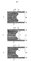
【解決手段】下地層上に、線幅が一定の線状部を有する第1のパターン14aと、第1のパターンの線状部に近接した部分と線状部から離れた部分を有し、第1のパターンとは独立して、又は第1のパターンに接続されて閉ループ形状を構成する第2のパターン14bとを形成する。第2のパターンの第1のパターンの線状部から離れた部分141aで閉ループカットを行う。
【選択図】図2
Description
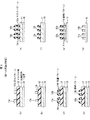
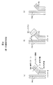
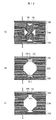
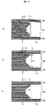
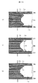
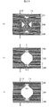
図1(a)〜(h)は、本発明の第1の実施の形態に係る半導体装置の製造工程を示す断面図、図2(a)〜(c)は、図1(d)に示す工程と図1(e)に示す工程との間に行われる閉ループカット工程を示す平面図である。
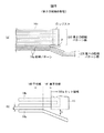
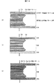
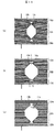
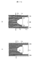
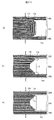
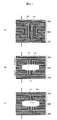
図3(a)〜(h)は、本発明の第2の実施の形態に係る半導体装置の製造工程を示す断面図、図4(a)〜(c)は、図3(h)の工程の後に行われる閉ループカット工程を示す平面図である。第1の実施の形態では、予め配線材料を形成しておき、側壁パターンの端部を閉ループカットした後に配線材料から配線パターンを形成したが、本実施の形態は、閉ループ形状の配線パターンを形成した後に配線パターンの端部を閉ループカットするものである。
Claims (5)
- 下地層上に、線幅が一定の線状部を有する第1のパターンと、前記第1のパターンの前記線状部に近接した部分と前記線状部から離れた部分を有し、前記第1のパターンとは独立して、又は前記第1のパターンに接続されて閉ループ形状を構成する第2のパターンとを形成する第1の工程と、
前記第2のパターンの前記第1のパターンの前記線状部から離れた部分で閉ループカットを行う第2の工程とを含む半導体装置の製造方法。 - 下地層上に、線幅が一定の線状部を有する第1のパターンと、前記第1のパターンの前記線状部との間に第1の間隔を有する、前記第1のパターンに平行な部分を備え、前記第1のパターンとは独立して、又は前記第1のパターンに接続されて閉ループ形状を構成する第2のパターンとを形成する第1の工程と、
前記第1のパターンの前記線状部との間に前記第1の間隔よりも大きい第2の間隔を有してレジストを前記第2のパターンの一部に形成し、前記レジストが形成された前記第2のパターンの部分で閉ループカットを行う第2の工程とを含む半導体装置の製造方法。 - 下地層上に、芯材パターンを形成し、前記芯材パターンの側面に側壁パターンを形成した後、前記芯材パターンを除去することにより、線幅が一定の線状部を有する閉ループ形状の第1のパターンと、前記第1のパターンの前記線状部に近接した部分と前記線状部から離れた部分とを有し、前記第1のパターンとは独立して、又は前記第1のパターンに接続されて閉ループ形状を構成する第2のパターンとを形成する第1の工程と、
前記第2のパターンの前記第1のパターンの前記線状部から離れた部分で閉ループカットを行う第2の工程とを含む半導体装置の製造方法。 - 下地層上に、所定の周期で配列された複数の第1のパターンからなる第1のパターン群と、前記所定の周期で配列された複数の第2のパターンからなり、前記複数の第2のパターンのうち、少なくとも前記第1の配線パターン群に最も近接する第2のパターンは、前記第1のパターン群に平行な平行部と、前記第2のパターン群から離れた部分とを有し、前記第1のパターン群とは独立して、又は前記第1のパターン群に接続されて閉ループ形状を構成する第2のパターン群とを形成する第1の工程と、
前記第2のパターンの前記第1のパターン群から離れた部分で閉ループカットを行う第2の工程とを含む半導体装置の製造方法。 - 所定の周期で配列された複数の第1の配線パターンからなる第1の配線パターン群と、
前記所定の周期で配列された複数の第2の配線パターンからなる第2の配線パターン群とを備え、
前記複数の第2の配線パターンのうち、少なくとも前記第1の配線パターン群に最も近接する第2の配線パターンは、前記第1の配線パターン群に平行な平行部と、前記平行部に接続して前記第1の配線パターン群から遠ざかるように設けられ、かつ前記第1の配線パターン群に平行でない非平行部とを有する半導体装置。
Priority Applications (3)
| Application Number | Priority Date | Filing Date | Title |
|---|---|---|---|
| JP2008209849A JP4789158B2 (ja) | 2008-08-18 | 2008-08-18 | 半導体装置の製造方法、及び半導体装置 |
| US12/542,540 US8183148B2 (en) | 2008-08-18 | 2009-08-17 | Method of fabricating semiconductor device and semiconductor device |
| US14/284,709 USRE46100E1 (en) | 2008-08-18 | 2014-05-22 | Method of fabricating semiconductor device and semiconductor device |
Applications Claiming Priority (1)
| Application Number | Priority Date | Filing Date | Title |
|---|---|---|---|
| JP2008209849A JP4789158B2 (ja) | 2008-08-18 | 2008-08-18 | 半導体装置の製造方法、及び半導体装置 |
Publications (2)
| Publication Number | Publication Date |
|---|---|
| JP2010045302A true JP2010045302A (ja) | 2010-02-25 |
| JP4789158B2 JP4789158B2 (ja) | 2011-10-12 |
Family
ID=41680751
Family Applications (1)
| Application Number | Title | Priority Date | Filing Date |
|---|---|---|---|
| JP2008209849A Active JP4789158B2 (ja) | 2008-08-18 | 2008-08-18 | 半導体装置の製造方法、及び半導体装置 |
Country Status (2)
| Country | Link |
|---|---|
| US (2) | US8183148B2 (ja) |
| JP (1) | JP4789158B2 (ja) |
Cited By (4)
| Publication number | Priority date | Publication date | Assignee | Title |
|---|---|---|---|---|
| KR20120017547A (ko) * | 2010-08-19 | 2012-02-29 | 삼성전자주식회사 | 라인 패턴 구조물의 형성 방법 |
| KR20130094169A (ko) * | 2012-02-15 | 2013-08-23 | 삼성전자주식회사 | 도전 라인의 전기적 접촉 신뢰성을 증가시키기 위해서 수정 직사각형 마스크 패턴을 이용하는 집적회로 장치 제조 방법 |
| US9653314B2 (en) | 2014-09-09 | 2017-05-16 | Kabushiki Kaisha Toshiba | Semiconductor device and manufacturing method thereof |
| KR101876941B1 (ko) * | 2011-12-22 | 2018-07-12 | 에스케이하이닉스 주식회사 | 반도체 소자의 제조 방법 |
Families Citing this family (8)
| Publication number | Priority date | Publication date | Assignee | Title |
|---|---|---|---|---|
| JP5395837B2 (ja) | 2011-03-24 | 2014-01-22 | 株式会社東芝 | 半導体装置の製造方法 |
| JP2013197266A (ja) | 2012-03-19 | 2013-09-30 | Toshiba Corp | 半導体装置およびその製造方法 |
| US8637982B2 (en) | 2012-04-18 | 2014-01-28 | Sandisk Technologies Inc. | Split loop cut pattern for spacer process |
| KR102059183B1 (ko) | 2013-03-07 | 2019-12-24 | 삼성전자주식회사 | 반도체 장치의 제조 방법 및 이에 의해 제조된 반도체 장치 |
| US9911693B2 (en) * | 2015-08-28 | 2018-03-06 | Micron Technology, Inc. | Semiconductor devices including conductive lines and methods of forming the semiconductor devices |
| US10483202B2 (en) * | 2016-02-22 | 2019-11-19 | Toshiba Memory Corporation | Semiconductor device having a wiring line with an end portion having rounded side surfaces and manufacturing method thereof |
| US9847339B2 (en) * | 2016-04-12 | 2017-12-19 | Macronix International Co., Ltd. | Self-aligned multiple patterning semiconductor device fabrication |
| CN108550522B (zh) * | 2018-04-27 | 2020-09-04 | 上海集成电路研发中心有限公司 | 一种多次图形化的方法 |
Citations (7)
| Publication number | Priority date | Publication date | Assignee | Title |
|---|---|---|---|---|
| JP2007081403A (ja) * | 2005-09-14 | 2007-03-29 | Hynix Semiconductor Inc | 半導体素子の微細パターン形成方法 |
| JP2008027991A (ja) * | 2006-07-18 | 2008-02-07 | Toshiba Corp | 半導体装置 |
| WO2008027239A2 (en) * | 2006-08-30 | 2008-03-06 | Micron Technology, Inc. | Single spacer process for multiplying pitch by a factor greater than two and related intermediate ic structures |
| JP2008535247A (ja) * | 2005-03-28 | 2008-08-28 | マイクロン テクノロジー, インク. | 集積回路製造 |
| JP2009076902A (ja) * | 2007-09-18 | 2009-04-09 | Hynix Semiconductor Inc | 半導体素子の微細パターン形成方法 |
| JP2009260309A (ja) * | 2008-04-17 | 2009-11-05 | Samsung Electronics Co Ltd | 半導体素子の微細パターン形成方法 |
| JP2010045359A (ja) * | 2008-08-11 | 2010-02-25 | Samsung Electronics Co Ltd | 半導体素子及び半導体素子のパターン形成方法 |
Family Cites Families (8)
| Publication number | Priority date | Publication date | Assignee | Title |
|---|---|---|---|---|
| US5328810A (en) * | 1990-05-07 | 1994-07-12 | Micron Technology, Inc. | Method for reducing, by a factor or 2-N, the minimum masking pitch of a photolithographic process |
| JPH0855908A (ja) | 1994-08-17 | 1996-02-27 | Toshiba Corp | 半導体装置 |
| JP3406302B2 (ja) * | 2001-01-16 | 2003-05-12 | 株式会社半導体先端テクノロジーズ | 微細パターンの形成方法、半導体装置の製造方法および半導体装置 |
| US6955961B1 (en) * | 2004-05-27 | 2005-10-18 | Macronix International Co., Ltd. | Method for defining a minimum pitch in an integrated circuit beyond photolithographic resolution |
| JP4936659B2 (ja) | 2004-12-27 | 2012-05-23 | 株式会社東芝 | 半導体装置の製造方法 |
| US7346887B2 (en) | 2005-11-09 | 2008-03-18 | International Business Machines Corporation | Method for fabricating integrated circuit features |
| JP4171032B2 (ja) | 2006-06-16 | 2008-10-22 | 株式会社東芝 | 半導体装置及びその製造方法 |
| JP4909735B2 (ja) | 2006-06-27 | 2012-04-04 | 株式会社東芝 | 不揮発性半導体メモリ |
-
2008
- 2008-08-18 JP JP2008209849A patent/JP4789158B2/ja active Active
-
2009
- 2009-08-17 US US12/542,540 patent/US8183148B2/en not_active Ceased
-
2014
- 2014-05-22 US US14/284,709 patent/USRE46100E1/en active Active
Patent Citations (7)
| Publication number | Priority date | Publication date | Assignee | Title |
|---|---|---|---|---|
| JP2008535247A (ja) * | 2005-03-28 | 2008-08-28 | マイクロン テクノロジー, インク. | 集積回路製造 |
| JP2007081403A (ja) * | 2005-09-14 | 2007-03-29 | Hynix Semiconductor Inc | 半導体素子の微細パターン形成方法 |
| JP2008027991A (ja) * | 2006-07-18 | 2008-02-07 | Toshiba Corp | 半導体装置 |
| WO2008027239A2 (en) * | 2006-08-30 | 2008-03-06 | Micron Technology, Inc. | Single spacer process for multiplying pitch by a factor greater than two and related intermediate ic structures |
| JP2009076902A (ja) * | 2007-09-18 | 2009-04-09 | Hynix Semiconductor Inc | 半導体素子の微細パターン形成方法 |
| JP2009260309A (ja) * | 2008-04-17 | 2009-11-05 | Samsung Electronics Co Ltd | 半導体素子の微細パターン形成方法 |
| JP2010045359A (ja) * | 2008-08-11 | 2010-02-25 | Samsung Electronics Co Ltd | 半導体素子及び半導体素子のパターン形成方法 |
Cited By (6)
| Publication number | Priority date | Publication date | Assignee | Title |
|---|---|---|---|---|
| KR20120017547A (ko) * | 2010-08-19 | 2012-02-29 | 삼성전자주식회사 | 라인 패턴 구조물의 형성 방법 |
| KR101692407B1 (ko) | 2010-08-19 | 2017-01-04 | 삼성전자주식회사 | 라인 패턴 구조물의 형성 방법 |
| KR101876941B1 (ko) * | 2011-12-22 | 2018-07-12 | 에스케이하이닉스 주식회사 | 반도체 소자의 제조 방법 |
| KR20130094169A (ko) * | 2012-02-15 | 2013-08-23 | 삼성전자주식회사 | 도전 라인의 전기적 접촉 신뢰성을 증가시키기 위해서 수정 직사각형 마스크 패턴을 이용하는 집적회로 장치 제조 방법 |
| KR101994245B1 (ko) | 2012-02-15 | 2019-06-28 | 삼성전자 주식회사 | 도전 라인의 전기적 접촉 신뢰성을 증가시키기 위해서 수정 직사각형 마스크 패턴을 이용하는 집적회로 장치 제조 방법 |
| US9653314B2 (en) | 2014-09-09 | 2017-05-16 | Kabushiki Kaisha Toshiba | Semiconductor device and manufacturing method thereof |
Also Published As
| Publication number | Publication date |
|---|---|
| US8183148B2 (en) | 2012-05-22 |
| USRE46100E1 (en) | 2016-08-09 |
| US20100038795A1 (en) | 2010-02-18 |
| JP4789158B2 (ja) | 2011-10-12 |
Similar Documents
| Publication | Publication Date | Title |
|---|---|---|
| JP4789158B2 (ja) | 半導体装置の製造方法、及び半導体装置 | |
| KR101618749B1 (ko) | 반도체 소자의 패턴 형성 방법 | |
| CN106847821B (zh) | 半导体结构及其形成方法 | |
| US8541316B2 (en) | Method of manufacturing semiconductor device including sequentially forming first and second mask material layers and forming a dotted photoresist pattern on the second mask material layer | |
| KR101314437B1 (ko) | 집적 회로 장치 및 그 제조 방법 | |
| US10186452B2 (en) | Asymmetric stair structure and method for fabricating the same | |
| JP2006186104A (ja) | 半導体装置およびその製造方法 | |
| US8765610B2 (en) | Method for manufacturing semiconductor device | |
| US9034765B2 (en) | Methods of forming a semiconductor device | |
| US8546196B2 (en) | Non-volatile memory device and manufacturing method thereof | |
| JP2013172070A (ja) | 半導体装置および半導体装置の製造方法 | |
| US20080124933A1 (en) | Fabrication process of a semiconductor device | |
| CN115997487B (zh) | 形成顶部选择栅极沟槽的方法 | |
| US8114778B2 (en) | Method of forming minute patterns in semiconductor device using double patterning | |
| TWI572016B (zh) | 半導體結構及其製造方法 | |
| TWI447809B (zh) | 凸出結構與形成凸出結構的方法 | |
| US8420453B2 (en) | Method of forming active region structure | |
| JP2013012620A (ja) | 半導体装置の製造方法 | |
| KR20140094352A (ko) | 벌집 형태의 반도체 소자의 패턴 형성 방법 | |
| JP2013239520A (ja) | 半導体装置及びその製造方法 | |
| CN114171376B (zh) | 一种半导体的图形制造方法 | |
| TWI506754B (zh) | 積體電路圖案及方法 | |
| US20130157384A1 (en) | Method for fabricating semiconductor device | |
| JP2023120043A (ja) | 不揮発性記憶装置及び不揮発性記憶装置の製造方法 | |
| TWI584443B (zh) | 接觸墊結構 |
Legal Events
| Date | Code | Title | Description |
|---|---|---|---|
| A621 | Written request for application examination |
Free format text: JAPANESE INTERMEDIATE CODE: A621 Effective date: 20100728 |
|
| RD03 | Notification of appointment of power of attorney |
Free format text: JAPANESE INTERMEDIATE CODE: A7423 Effective date: 20100927 |
|
| A977 | Report on retrieval |
Free format text: JAPANESE INTERMEDIATE CODE: A971007 Effective date: 20110126 |
|
| A131 | Notification of reasons for refusal |
Free format text: JAPANESE INTERMEDIATE CODE: A131 Effective date: 20110128 |
|
| A521 | Request for written amendment filed |
Free format text: JAPANESE INTERMEDIATE CODE: A523 Effective date: 20110309 |
|
| A131 | Notification of reasons for refusal |
Free format text: JAPANESE INTERMEDIATE CODE: A131 Effective date: 20110405 |
|
| A521 | Request for written amendment filed |
Free format text: JAPANESE INTERMEDIATE CODE: A523 Effective date: 20110523 |
|
| TRDD | Decision of grant or rejection written | ||
| A01 | Written decision to grant a patent or to grant a registration (utility model) |
Free format text: JAPANESE INTERMEDIATE CODE: A01 Effective date: 20110621 |
|
| A01 | Written decision to grant a patent or to grant a registration (utility model) |
Free format text: JAPANESE INTERMEDIATE CODE: A01 |
|
| RD04 | Notification of resignation of power of attorney |
Free format text: JAPANESE INTERMEDIATE CODE: A7424 Effective date: 20110627 |
|
| RD04 | Notification of resignation of power of attorney |
Free format text: JAPANESE INTERMEDIATE CODE: A7424 Effective date: 20110628 |
|
| RD04 | Notification of resignation of power of attorney |
Free format text: JAPANESE INTERMEDIATE CODE: A7424 Effective date: 20110629 |
|
| RD04 | Notification of resignation of power of attorney |
Free format text: JAPANESE INTERMEDIATE CODE: A7424 Effective date: 20110630 |
|
| A61 | First payment of annual fees (during grant procedure) |
Free format text: JAPANESE INTERMEDIATE CODE: A61 Effective date: 20110713 |
|
| FPAY | Renewal fee payment (event date is renewal date of database) |
Free format text: PAYMENT UNTIL: 20140729 Year of fee payment: 3 |
|
| R151 | Written notification of patent or utility model registration |
Ref document number: 4789158 Country of ref document: JP Free format text: JAPANESE INTERMEDIATE CODE: R151 |
|
| S111 | Request for change of ownership or part of ownership |
Free format text: JAPANESE INTERMEDIATE CODE: R313111 |
|
| R350 | Written notification of registration of transfer |
Free format text: JAPANESE INTERMEDIATE CODE: R350 |
|
| S111 | Request for change of ownership or part of ownership |
Free format text: JAPANESE INTERMEDIATE CODE: R313111 |
|
| R350 | Written notification of registration of transfer |
Free format text: JAPANESE INTERMEDIATE CODE: R350 |