JP2010040076A - 不揮発性半導体記憶装置および不揮発性半導体記憶システム - Google Patents
不揮発性半導体記憶装置および不揮発性半導体記憶システム Download PDFInfo
- Publication number
- JP2010040076A JP2010040076A JP2008199707A JP2008199707A JP2010040076A JP 2010040076 A JP2010040076 A JP 2010040076A JP 2008199707 A JP2008199707 A JP 2008199707A JP 2008199707 A JP2008199707 A JP 2008199707A JP 2010040076 A JP2010040076 A JP 2010040076A
- Authority
- JP
- Japan
- Prior art keywords
- power supply
- data
- power
- voltage
- semiconductor memory
- Prior art date
- Legal status (The legal status is an assumption and is not a legal conclusion. Google has not performed a legal analysis and makes no representation as to the accuracy of the status listed.)
- Granted
Links
Images


Classifications
-
- G—PHYSICS
- G11—INFORMATION STORAGE
- G11C—STATIC STORES
- G11C16/00—Erasable programmable read-only memories
- G11C16/02—Erasable programmable read-only memories electrically programmable
- G11C16/06—Auxiliary circuits, e.g. for writing into memory
- G11C16/30—Power supply circuits
-
- G—PHYSICS
- G11—INFORMATION STORAGE
- G11C—STATIC STORES
- G11C16/00—Erasable programmable read-only memories
- G11C16/02—Erasable programmable read-only memories electrically programmable
- G11C16/04—Erasable programmable read-only memories electrically programmable using variable threshold transistors, e.g. FAMOS
- G11C16/0483—Erasable programmable read-only memories electrically programmable using variable threshold transistors, e.g. FAMOS comprising cells having several storage transistors connected in series
-
- G—PHYSICS
- G11—INFORMATION STORAGE
- G11C—STATIC STORES
- G11C5/00—Details of stores covered by group G11C11/00
- G11C5/14—Power supply arrangements, e.g. power down, chip selection or deselection, layout of wirings or power grids, or multiple supply levels
- G11C5/143—Detection of memory cassette insertion or removal; Continuity checks of supply or ground lines; Detection of supply variations, interruptions or levels ; Switching between alternative supplies
-
- G—PHYSICS
- G11—INFORMATION STORAGE
- G11C—STATIC STORES
- G11C5/00—Details of stores covered by group G11C11/00
- G11C5/14—Power supply arrangements, e.g. power down, chip selection or deselection, layout of wirings or power grids, or multiple supply levels
- G11C5/145—Applications of charge pumps; Boosted voltage circuits; Clamp circuits therefor
-
- G—PHYSICS
- G11—INFORMATION STORAGE
- G11C—STATIC STORES
- G11C8/00—Arrangements for selecting an address in a digital store
- G11C8/06—Address interface arrangements, e.g. address buffers
-
- G—PHYSICS
- G11—INFORMATION STORAGE
- G11C—STATIC STORES
- G11C8/00—Arrangements for selecting an address in a digital store
- G11C8/10—Decoders
Landscapes
- Engineering & Computer Science (AREA)
- Microelectronics & Electronic Packaging (AREA)
- Power Engineering (AREA)
- Read Only Memory (AREA)
Abstract
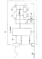
【解決手段】半導体記憶装置は、不揮発性メモリセルと、データを検出しあるいはデータを書き込むセンスアンプと、複数のビット線から或るビット線を選択するカラムデコーダと、複数のワード線から或るワード線を選択するロウデコーダと、センスアンプ、カラムデコーダおよびロウデコーダに電力供給するチャージポンプと、データ読出しまたはデータ書込み対象であるメモリセルを選択するアドレスに基づいてセンスアンプ、カラムデコーダおよびロウデコーダを制御する論理回路と、論理回路に電圧を印加する第1の電源入力と、チャージポンプに第1の電源入力の電圧より高い電圧を印加する第2の電源入力であって、少なくともデータ読出しおよびデータ書込み時にチャージポンプに電力供給する第2の電源入力とを備えている。
【選択図】図1
Description
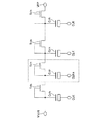
図7は、本発明に係る第2の実施形態に従ったメモリシステムの構成を示すブロック図である。このメモリシステム201は、複数のフラッシュメモリ101‐1〜101‐4を搭載する。図7では、4個のメモリチップを搭載しているが、5個以上のメモリチップを搭載してもよいし、3個以下であってもよい。フラッシュメモリ101‐1〜101‐4は、それぞれ図1に示すフラッシュメモリ101と同じ構成を有する。
Claims (5)
- 複数のワード線と、
複数のビット線と、
前記ワード線と前記ビット線との交点に対応して設けられ、データを電気的に記憶する複数の不揮発性メモリセルと、
前記メモリセルのデータを検出し、あるいは、前記メモリセルへデータを書き込むために前記ビット線を駆動するセンスアンプと、
前記センスアンプが読出しデータを出力し、あるいは、書込みデータを受け取るために、前記複数のビット線から或るビット線を選択するカラムデコーダと、
前記複数のワード線から或るワード線を選択するロウデコーダと、
前記センスアンプ、前記カラムデコーダおよび前記ロウデコーダに電力供給するチャージポンプと、
データ読出しまたはデータ書込み対象である前記メモリセルを選択するアドレスに基づいて前記センスアンプ、前記カラムデコーダおよび前記ロウデコーダを制御する論理回路と、
前記論理回路に電圧を印加する第1の電源入力と、
前記チャージポンプに前記第1の電源入力の電圧より高い電圧を印加する第2の電源入力であって、少なくともデータ読出しおよびデータ書込み時に前記チャージポンプに電力供給する第2の電源入力とを備えた不揮発性半導体記憶装置。 - 前記第1の電源入力は、JEITAの3.3V電源電圧仕様(ED−5001A)におけるノーマルレンジ(3.3±0.3V)またはワイドレンジ(2.7〜3.6V)に準拠する電源から電力供給を受け、
前記第2の電源入力は、ATXの5V電源電圧仕様に準拠する電源から電力供給を受けることを特徴とする請求項1に記載の不揮発性半導体記憶装置。 - 前記第1の電源入力は、JEITAの1.8V電源電圧仕様(ED−5003A)におけるノーマルレンジ(1.8±0.15V)またはワイドレンジ(1.2〜1.95V)に準拠する電源から電力供給を受け、
前記第2の電源入力は、ATXの5V電源電圧仕様に準拠する電源から電力供給を受けることを特徴とする請求項1に記載の不揮発性半導体記憶装置。 - 前記第2の電源入力は、ハードディスクドライブ(HDD)用の電源と同一電圧電源から電力供給を受けることを特徴とする請求項1から請求項3のいずれかに記載の半導体記憶装置。
- データ書込みあるいはデータ読出し対象となる前記メモリセルの情報を格納するキャッシュをさらに備え、
データ書込みまたはデータ読出し動作において、データ書込みあるいはデータ読出し対象となる前記メモリセルの情報を前記キャッシュに格納する初期化動作と、前記チャージポンプによる前記第2の電源の電圧の昇圧動作とを同時に実行することを特徴とする請求項1から請求項4のいずれかに記載の不揮発性半導体記憶装置。
Priority Applications (2)
| Application Number | Priority Date | Filing Date | Title |
|---|---|---|---|
| JP2008199707A JP5331405B2 (ja) | 2008-08-01 | 2008-08-01 | 不揮発性半導体記憶装置および不揮発性半導体記憶システム |
| US12/533,529 US7986557B2 (en) | 2008-08-01 | 2009-07-31 | Nonvolatile semiconductor memory device and nonvolatile semiconductor memory system |
Applications Claiming Priority (1)
| Application Number | Priority Date | Filing Date | Title |
|---|---|---|---|
| JP2008199707A JP5331405B2 (ja) | 2008-08-01 | 2008-08-01 | 不揮発性半導体記憶装置および不揮発性半導体記憶システム |
Publications (2)
| Publication Number | Publication Date |
|---|---|
| JP2010040076A true JP2010040076A (ja) | 2010-02-18 |
| JP5331405B2 JP5331405B2 (ja) | 2013-10-30 |
Family
ID=41608214
Family Applications (1)
| Application Number | Title | Priority Date | Filing Date |
|---|---|---|---|
| JP2008199707A Active JP5331405B2 (ja) | 2008-08-01 | 2008-08-01 | 不揮発性半導体記憶装置および不揮発性半導体記憶システム |
Country Status (2)
| Country | Link |
|---|---|
| US (1) | US7986557B2 (ja) |
| JP (1) | JP5331405B2 (ja) |
Cited By (1)
| Publication number | Priority date | Publication date | Assignee | Title |
|---|---|---|---|---|
| JP2012150857A (ja) * | 2011-01-17 | 2012-08-09 | Toshiba Corp | 電源回路 |
Families Citing this family (7)
| Publication number | Priority date | Publication date | Assignee | Title |
|---|---|---|---|---|
| US8644073B2 (en) * | 2011-02-28 | 2014-02-04 | Stmicroelectronics S.R.L. | Non-volatile memory device with improved programming management and related method |
| US9224480B2 (en) * | 2013-02-27 | 2015-12-29 | Texas Instruments Incorporated | Dual-function read/write cache for programmable non-volatile memory |
| US9202579B2 (en) * | 2013-03-14 | 2015-12-01 | Sandisk Technologies Inc. | Compensation for temperature dependence of bit line resistance |
| KR102138936B1 (ko) | 2013-11-11 | 2020-07-28 | 삼성전자주식회사 | 전력 공급 장치 및 그것을 이용한 전력 공급 방법 |
| KR102546531B1 (ko) | 2019-04-02 | 2023-06-21 | 삼성전자주식회사 | 자기 메모리 장치 |
| US11081149B1 (en) * | 2020-03-31 | 2021-08-03 | Winbond Electronics Corp. | Memory device for artificial intelligence operation |
| CN119495342A (zh) * | 2023-08-14 | 2025-02-21 | 长江存储科技有限责任公司 | 一种存储器及其操作方法、存储器系统和可读存储介质 |
Citations (3)
| Publication number | Priority date | Publication date | Assignee | Title |
|---|---|---|---|---|
| JP2000509875A (ja) * | 1997-01-08 | 2000-08-02 | マイクロン・テクノロジー・インコーポレーテッド | 不揮発性メモリ・システム内でのプログラミング電圧保護 |
| JP2008017203A (ja) * | 2006-07-06 | 2008-01-24 | Renesas Technology Corp | 半導体集積回路装置 |
| WO2008098350A1 (en) * | 2007-02-16 | 2008-08-21 | Mosaid Technologies Incorporated | Non-volatile semiconductor memory having multiple external power supplies |
Family Cites Families (6)
| Publication number | Priority date | Publication date | Assignee | Title |
|---|---|---|---|---|
| KR100299254B1 (ko) * | 1994-10-19 | 2001-09-03 | 피터 엔. 데트킨 | 플래시메모리용전압공급기 |
| US6208542B1 (en) * | 1998-06-30 | 2001-03-27 | Sandisk Corporation | Techniques for storing digital data in an analog or multilevel memory |
| US6160440A (en) * | 1998-09-25 | 2000-12-12 | Intel Corporation | Scaleable charge pump for use with a low voltage power supply |
| US6977842B2 (en) * | 2003-09-16 | 2005-12-20 | Micron Technology, Inc. | Boosted substrate/tub programming for flash memories |
| JP4908064B2 (ja) * | 2005-08-19 | 2012-04-04 | 株式会社東芝 | 半導体集積回路装置 |
| JP2009003991A (ja) * | 2007-06-19 | 2009-01-08 | Toshiba Corp | 半導体装置及び半導体メモリテスト装置 |
-
2008
- 2008-08-01 JP JP2008199707A patent/JP5331405B2/ja active Active
-
2009
- 2009-07-31 US US12/533,529 patent/US7986557B2/en active Active
Patent Citations (3)
| Publication number | Priority date | Publication date | Assignee | Title |
|---|---|---|---|---|
| JP2000509875A (ja) * | 1997-01-08 | 2000-08-02 | マイクロン・テクノロジー・インコーポレーテッド | 不揮発性メモリ・システム内でのプログラミング電圧保護 |
| JP2008017203A (ja) * | 2006-07-06 | 2008-01-24 | Renesas Technology Corp | 半導体集積回路装置 |
| WO2008098350A1 (en) * | 2007-02-16 | 2008-08-21 | Mosaid Technologies Incorporated | Non-volatile semiconductor memory having multiple external power supplies |
Cited By (2)
| Publication number | Priority date | Publication date | Assignee | Title |
|---|---|---|---|---|
| JP2012150857A (ja) * | 2011-01-17 | 2012-08-09 | Toshiba Corp | 電源回路 |
| US8659968B2 (en) | 2011-01-17 | 2014-02-25 | Kabushiki Kaisha Toshiba | Power supply circuit and semiconductor memory device including the power supply circuit |
Also Published As
| Publication number | Publication date |
|---|---|
| US20100027341A1 (en) | 2010-02-04 |
| JP5331405B2 (ja) | 2013-10-30 |
| US7986557B2 (en) | 2011-07-26 |
Similar Documents
| Publication | Publication Date | Title |
|---|---|---|
| JP5331405B2 (ja) | 不揮発性半導体記憶装置および不揮発性半導体記憶システム | |
| US12373143B2 (en) | Memory device | |
| US8923047B2 (en) | Semiconductor memory device | |
| US20150036435A1 (en) | Nonvolatile memory device, memory system including the same, and method of operating nonvolatile memory device | |
| US10403374B2 (en) | Reduction of output voltage ripple in booster circuit | |
| KR20100117560A (ko) | 설정 변경 가능한 페이지 사이즈를 갖는 비휘발성 메모리 장치 | |
| JP6482690B1 (ja) | 半導体記憶装置 | |
| JP5249394B2 (ja) | 半導体記憶装置 | |
| KR102277111B1 (ko) | 반도체 기억 장치 | |
| JP2007035246A (ja) | プログラム速度を向上させることができるフラッシュメモリ装置及びそれのプログラム方法 | |
| US20140269127A1 (en) | Memory Operation Latency Control | |
| KR20120049509A (ko) | 로우 디코더 회로 및 이를 포함하는 비휘발성 메모리 장치 | |
| JP2021163511A (ja) | 半導体記憶装置 | |
| JP2021121982A (ja) | メモリ装置におけるプログラム禁止 | |
| US9865358B2 (en) | Flash memory device and erase method thereof capable of reducing power consumption | |
| JP5468224B2 (ja) | フラッシュメモリ装置及びそのプログラム方法 | |
| KR102861570B1 (ko) | 페이지 버퍼를 포함하는 메모리 장치 | |
| JP2013191264A (ja) | 半導体記憶装置およびその駆動方法 | |
| US8238156B2 (en) | Nonvolatile semiconductor memory device and method of operating the same | |
| JP2023032169A (ja) | 半導体記憶装置及びメモリシステム | |
| JP4828520B2 (ja) | 半導体装置およびその制御方法 | |
| US12315573B2 (en) | Method and apparatus to reduce power consumption of page buffer circuitry in a non-volatile memory device | |
| JP2025002640A (ja) | 半導体記憶装置、及び、データ消去方法 | |
| US20220270691A1 (en) | Semiconductor storage device | |
| JP2004014052A (ja) | 不揮発性半導体記憶装置 |
Legal Events
| Date | Code | Title | Description |
|---|---|---|---|
| A621 | Written request for application examination |
Free format text: JAPANESE INTERMEDIATE CODE: A621 Effective date: 20100803 |
|
| A977 | Report on retrieval |
Free format text: JAPANESE INTERMEDIATE CODE: A971007 Effective date: 20121107 |
|
| A131 | Notification of reasons for refusal |
Free format text: JAPANESE INTERMEDIATE CODE: A131 Effective date: 20121113 |
|
| TRDD | Decision of grant or rejection written | ||
| A01 | Written decision to grant a patent or to grant a registration (utility model) |
Free format text: JAPANESE INTERMEDIATE CODE: A01 Effective date: 20130705 |
|
| A61 | First payment of annual fees (during grant procedure) |
Free format text: JAPANESE INTERMEDIATE CODE: A61 Effective date: 20130729 |
|
| R151 | Written notification of patent or utility model registration |
Ref document number: 5331405 Country of ref document: JP Free format text: JAPANESE INTERMEDIATE CODE: R151 |
|
| S111 | Request for change of ownership or part of ownership |
Free format text: JAPANESE INTERMEDIATE CODE: R313111 |
|
| R350 | Written notification of registration of transfer |
Free format text: JAPANESE INTERMEDIATE CODE: R350 |
|
| S111 | Request for change of ownership or part of ownership |
Free format text: JAPANESE INTERMEDIATE CODE: R313111 |
|
| R350 | Written notification of registration of transfer |
Free format text: JAPANESE INTERMEDIATE CODE: R350 |