JP2010010224A - 半導体装置及びその製造方法 - Google Patents
半導体装置及びその製造方法 Download PDFInfo
- Publication number
- JP2010010224A JP2010010224A JP2008164892A JP2008164892A JP2010010224A JP 2010010224 A JP2010010224 A JP 2010010224A JP 2008164892 A JP2008164892 A JP 2008164892A JP 2008164892 A JP2008164892 A JP 2008164892A JP 2010010224 A JP2010010224 A JP 2010010224A
- Authority
- JP
- Japan
- Prior art keywords
- film
- metal
- metal film
- semiconductor region
- gate electrode
- Prior art date
- Legal status (The legal status is an assumption and is not a legal conclusion. Google has not performed a legal analysis and makes no representation as to the accuracy of the status listed.)
- Pending
Links
Images


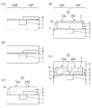


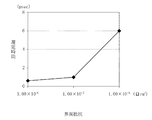
Classifications
-
- H—ELECTRICITY
- H10—SEMICONDUCTOR DEVICES; ELECTRIC SOLID-STATE DEVICES NOT OTHERWISE PROVIDED FOR
- H10D—INORGANIC ELECTRIC SEMICONDUCTOR DEVICES
- H10D84/00—Integrated devices formed in or on semiconductor substrates that comprise only semiconducting layers, e.g. on Si wafers or on GaAs-on-Si wafers
- H10D84/01—Manufacture or treatment
- H10D84/0123—Integrating together multiple components covered by H10D12/00 or H10D30/00, e.g. integrating multiple IGBTs
- H10D84/0126—Integrating together multiple components covered by H10D12/00 or H10D30/00, e.g. integrating multiple IGBTs the components including insulated gates, e.g. IGFETs
- H10D84/0165—Integrating together multiple components covered by H10D12/00 or H10D30/00, e.g. integrating multiple IGBTs the components including insulated gates, e.g. IGFETs the components including complementary IGFETs, e.g. CMOS devices
- H10D84/0172—Manufacturing their gate conductors
- H10D84/0177—Manufacturing their gate conductors the gate conductors having different materials or different implants
-
- H—ELECTRICITY
- H10—SEMICONDUCTOR DEVICES; ELECTRIC SOLID-STATE DEVICES NOT OTHERWISE PROVIDED FOR
- H10D—INORGANIC ELECTRIC SEMICONDUCTOR DEVICES
- H10D84/00—Integrated devices formed in or on semiconductor substrates that comprise only semiconducting layers, e.g. on Si wafers or on GaAs-on-Si wafers
- H10D84/01—Manufacture or treatment
- H10D84/02—Manufacture or treatment characterised by using material-based technologies
- H10D84/03—Manufacture or treatment characterised by using material-based technologies using Group IV technology, e.g. silicon technology or silicon-carbide [SiC] technology
- H10D84/038—Manufacture or treatment characterised by using material-based technologies using Group IV technology, e.g. silicon technology or silicon-carbide [SiC] technology using silicon technology, e.g. SiGe
-
- H—ELECTRICITY
- H10—SEMICONDUCTOR DEVICES; ELECTRIC SOLID-STATE DEVICES NOT OTHERWISE PROVIDED FOR
- H10D—INORGANIC ELECTRIC SEMICONDUCTOR DEVICES
- H10D64/00—Electrodes of devices having potential barriers
- H10D64/01—Manufacture or treatment
- H10D64/013—Manufacture or treatment of electrodes having a conductor capacitively coupled to a semiconductor by an insulator
- H10D64/01302—Manufacture or treatment of electrodes having a conductor capacitively coupled to a semiconductor by an insulator the insulator being formed after the semiconductor body, the semiconductor being silicon
- H10D64/01304—Manufacture or treatment of electrodes having a conductor capacitively coupled to a semiconductor by an insulator the insulator being formed after the semiconductor body, the semiconductor being silicon characterised by the conductor
- H10D64/01306—Manufacture or treatment of electrodes having a conductor capacitively coupled to a semiconductor by an insulator the insulator being formed after the semiconductor body, the semiconductor being silicon characterised by the conductor the conductor comprising a layer of silicon contacting the insulator, e.g. polysilicon
- H10D64/01308—Manufacture or treatment of electrodes having a conductor capacitively coupled to a semiconductor by an insulator the insulator being formed after the semiconductor body, the semiconductor being silicon characterised by the conductor the conductor comprising a layer of silicon contacting the insulator, e.g. polysilicon the conductor further comprising a non-elemental silicon additional conductive layer, e.g. a metal silicide layer formed by the reaction of silicon with an implanted metal
- H10D64/0131—Manufacture or treatment of electrodes having a conductor capacitively coupled to a semiconductor by an insulator the insulator being formed after the semiconductor body, the semiconductor being silicon characterised by the conductor the conductor comprising a layer of silicon contacting the insulator, e.g. polysilicon the conductor further comprising a non-elemental silicon additional conductive layer, e.g. a metal silicide layer formed by the reaction of silicon with an implanted metal the additional conductive layer comprising a silicide layer formed by the silicidation reaction between the layer of silicon with a metal layer which is not formed by metal implantation
-
- H—ELECTRICITY
- H10—SEMICONDUCTOR DEVICES; ELECTRIC SOLID-STATE DEVICES NOT OTHERWISE PROVIDED FOR
- H10D—INORGANIC ELECTRIC SEMICONDUCTOR DEVICES
- H10D64/00—Electrodes of devices having potential barriers
- H10D64/01—Manufacture or treatment
- H10D64/013—Manufacture or treatment of electrodes having a conductor capacitively coupled to a semiconductor by an insulator
- H10D64/01302—Manufacture or treatment of electrodes having a conductor capacitively coupled to a semiconductor by an insulator the insulator being formed after the semiconductor body, the semiconductor being silicon
- H10D64/01304—Manufacture or treatment of electrodes having a conductor capacitively coupled to a semiconductor by an insulator the insulator being formed after the semiconductor body, the semiconductor being silicon characterised by the conductor
- H10D64/01318—Manufacture or treatment of electrodes having a conductor capacitively coupled to a semiconductor by an insulator the insulator being formed after the semiconductor body, the semiconductor being silicon characterised by the conductor the conductor comprising a layer of alloy material, compound material or organic material contacting the insulator, e.g. TiN
-
- H—ELECTRICITY
- H10—SEMICONDUCTOR DEVICES; ELECTRIC SOLID-STATE DEVICES NOT OTHERWISE PROVIDED FOR
- H10D—INORGANIC ELECTRIC SEMICONDUCTOR DEVICES
- H10D64/00—Electrodes of devices having potential barriers
- H10D64/60—Electrodes characterised by their materials
- H10D64/66—Electrodes having a conductor capacitively coupled to a semiconductor by an insulator, e.g. MIS electrodes
- H10D64/661—Electrodes having a conductor capacitively coupled to a semiconductor by an insulator, e.g. MIS electrodes the conductor comprising a layer of silicon contacting the insulator, e.g. polysilicon having vertical doping variation
- H10D64/662—Electrodes having a conductor capacitively coupled to a semiconductor by an insulator, e.g. MIS electrodes the conductor comprising a layer of silicon contacting the insulator, e.g. polysilicon having vertical doping variation the conductor further comprising additional layers, e.g. multiple silicon layers having different crystal structures
-
- H—ELECTRICITY
- H10—SEMICONDUCTOR DEVICES; ELECTRIC SOLID-STATE DEVICES NOT OTHERWISE PROVIDED FOR
- H10D—INORGANIC ELECTRIC SEMICONDUCTOR DEVICES
- H10D64/00—Electrodes of devices having potential barriers
- H10D64/60—Electrodes characterised by their materials
- H10D64/66—Electrodes having a conductor capacitively coupled to a semiconductor by an insulator, e.g. MIS electrodes
- H10D64/667—Electrodes having a conductor capacitively coupled to a semiconductor by an insulator, e.g. MIS electrodes the conductor comprising a layer of alloy material, compound material or organic material contacting the insulator, e.g. TiN workfunction layers
-
- H—ELECTRICITY
- H10—SEMICONDUCTOR DEVICES; ELECTRIC SOLID-STATE DEVICES NOT OTHERWISE PROVIDED FOR
- H10W—GENERIC PACKAGES, INTERCONNECTIONS, CONNECTORS OR OTHER CONSTRUCTIONAL DETAILS OF DEVICES COVERED BY CLASS H10
- H10W20/00—Interconnections in chips, wafers or substrates
- H10W20/40—Interconnections external to wafers or substrates, e.g. back-end-of-line [BEOL] metallisations or vias connecting to gate electrodes
Landscapes
- Electrodes Of Semiconductors (AREA)
- Metal-Oxide And Bipolar Metal-Oxide Semiconductor Integrated Circuits (AREA)
- Insulated Gate Type Field-Effect Transistor (AREA)
- Internal Circuitry In Semiconductor Integrated Circuit Devices (AREA)
Priority Applications (3)
| Application Number | Priority Date | Filing Date | Title |
|---|---|---|---|
| JP2008164892A JP2010010224A (ja) | 2008-06-24 | 2008-06-24 | 半導体装置及びその製造方法 |
| PCT/JP2009/000827 WO2009157113A1 (ja) | 2008-06-24 | 2009-02-25 | 半導体装置及びその製造方法 |
| US12/712,688 US8004046B2 (en) | 2008-06-24 | 2010-02-25 | Semiconductor device and method for fabricating the same |
Applications Claiming Priority (1)
| Application Number | Priority Date | Filing Date | Title |
|---|---|---|---|
| JP2008164892A JP2010010224A (ja) | 2008-06-24 | 2008-06-24 | 半導体装置及びその製造方法 |
Publications (2)
| Publication Number | Publication Date |
|---|---|
| JP2010010224A true JP2010010224A (ja) | 2010-01-14 |
| JP2010010224A5 JP2010010224A5 (enExample) | 2010-04-02 |
Family
ID=41444186
Family Applications (1)
| Application Number | Title | Priority Date | Filing Date |
|---|---|---|---|
| JP2008164892A Pending JP2010010224A (ja) | 2008-06-24 | 2008-06-24 | 半導体装置及びその製造方法 |
Country Status (3)
| Country | Link |
|---|---|
| US (1) | US8004046B2 (enExample) |
| JP (1) | JP2010010224A (enExample) |
| WO (1) | WO2009157113A1 (enExample) |
Families Citing this family (3)
| Publication number | Priority date | Publication date | Assignee | Title |
|---|---|---|---|---|
| JP2011071402A (ja) * | 2009-09-28 | 2011-04-07 | Panasonic Corp | 半導体装置の製造方法及びそれを用いた半導体装置 |
| US8378428B2 (en) * | 2010-09-29 | 2013-02-19 | Taiwan Semiconductor Manufacturing Company, Ltd. | Metal gate structure of a semiconductor device |
| US9041114B2 (en) * | 2013-05-20 | 2015-05-26 | Kabushiki Kaisha Toshiba | Contact plug penetrating a metallic transistor |
Citations (5)
| Publication number | Priority date | Publication date | Assignee | Title |
|---|---|---|---|---|
| JPH05206461A (ja) * | 1992-01-14 | 1993-08-13 | Nec Corp | 半導体装置の製造方法 |
| WO2001071807A1 (en) * | 2000-03-24 | 2001-09-27 | Fujitsu Limited | Semiconductor device and method of manufacture thereof |
| JP2005236120A (ja) * | 2004-02-20 | 2005-09-02 | Oki Electric Ind Co Ltd | 半導体装置及びその製造方法 |
| JP2006237372A (ja) * | 2005-02-25 | 2006-09-07 | Toshiba Corp | 半導体装置 |
| JP2006523008A (ja) * | 2001-05-26 | 2006-10-05 | フリースケール セミコンダクター インコーポレイテッド | 半導体素子とその作製法 |
Family Cites Families (5)
| Publication number | Priority date | Publication date | Assignee | Title |
|---|---|---|---|---|
| JP3394022B2 (ja) | 1999-08-16 | 2003-04-07 | 松下電器産業株式会社 | 半導体装置及びその製造方法 |
| JP3247099B2 (ja) | 2000-01-20 | 2002-01-15 | 松下電器産業株式会社 | 電極構造体の形成方法及び半導体装置の製造方法 |
| US6509254B1 (en) | 2000-01-20 | 2003-01-21 | Matsushita Electric Industrial Co., Ltd. | Method of forming electrode structure and method of fabricating semiconductor device |
| JP2007088122A (ja) | 2005-09-21 | 2007-04-05 | Renesas Technology Corp | 半導体装置 |
| KR100741857B1 (ko) | 2006-05-03 | 2007-07-24 | 삼성전자주식회사 | 계면 저항을 줄일 수 있는 게이트 콘택 구조체를 구비하는반도체 장치 및 그 제조 방법 |
-
2008
- 2008-06-24 JP JP2008164892A patent/JP2010010224A/ja active Pending
-
2009
- 2009-02-25 WO PCT/JP2009/000827 patent/WO2009157113A1/ja not_active Ceased
-
2010
- 2010-02-25 US US12/712,688 patent/US8004046B2/en not_active Expired - Fee Related
Patent Citations (5)
| Publication number | Priority date | Publication date | Assignee | Title |
|---|---|---|---|---|
| JPH05206461A (ja) * | 1992-01-14 | 1993-08-13 | Nec Corp | 半導体装置の製造方法 |
| WO2001071807A1 (en) * | 2000-03-24 | 2001-09-27 | Fujitsu Limited | Semiconductor device and method of manufacture thereof |
| JP2006523008A (ja) * | 2001-05-26 | 2006-10-05 | フリースケール セミコンダクター インコーポレイテッド | 半導体素子とその作製法 |
| JP2005236120A (ja) * | 2004-02-20 | 2005-09-02 | Oki Electric Ind Co Ltd | 半導体装置及びその製造方法 |
| JP2006237372A (ja) * | 2005-02-25 | 2006-09-07 | Toshiba Corp | 半導体装置 |
Also Published As
| Publication number | Publication date |
|---|---|
| US8004046B2 (en) | 2011-08-23 |
| US20100148281A1 (en) | 2010-06-17 |
| WO2009157113A1 (ja) | 2009-12-30 |
Similar Documents
| Publication | Publication Date | Title |
|---|---|---|
| US12046657B2 (en) | Method of manufacturing a semiconductor device including capping layer, barrier layer and work function layer | |
| US7601623B2 (en) | Method of manufacturing a semiconductor device with a gate electrode having a laminate structure | |
| JP4459257B2 (ja) | 半導体装置 | |
| US8546212B2 (en) | Semiconductor device and fabricating method thereof | |
| US8581351B2 (en) | Replacement gate with reduced gate leakage current | |
| US20150349080A1 (en) | FinFETs with Multiple Threshold Voltages | |
| US8384166B2 (en) | Method for manufacturing semiconductor device and semiconductor device | |
| JP2009290200A (ja) | 二重仕事関数半導体デバイスおよびその製造方法 | |
| TWI612666B (zh) | 一種製作鰭狀場效電晶體的方法 | |
| TWI525714B (zh) | 雙工作函數半導體元件及其形成方法 | |
| US9231084B2 (en) | Method of forming laterally diffused metal oxide semiconductor transistor with partially unsilicided source/drain | |
| WO2009157113A1 (ja) | 半導体装置及びその製造方法 | |
| CN102856256B (zh) | 半导体元件及其制作方法 | |
| TWI509702B (zh) | 具有金屬閘極之電晶體及其製作方法 | |
| KR100729367B1 (ko) | 반도체 장치 및 그 제조 방법 | |
| US20080179687A1 (en) | Semiconductor device and method for manufacturing the same | |
| TWI490949B (zh) | 具有金屬閘極之電晶體及其製作方法 | |
| JP2010010223A (ja) | 半導体装置及びその製造方法 | |
| JP2011071402A (ja) | 半導体装置の製造方法及びそれを用いた半導体装置 | |
| JP2012231071A (ja) | 半導体装置及びその製造方法 | |
| KR20100037969A (ko) | P형 금속게이트전극을 갖는 cmos장치 및 그 제조 방법 | |
| KR20100051137A (ko) | 반도체 소자 및 그 제조 방법. |
Legal Events
| Date | Code | Title | Description |
|---|---|---|---|
| A521 | Request for written amendment filed |
Free format text: JAPANESE INTERMEDIATE CODE: A523 Effective date: 20100210 |
|
| A621 | Written request for application examination |
Free format text: JAPANESE INTERMEDIATE CODE: A621 Effective date: 20100210 |
|
| RD02 | Notification of acceptance of power of attorney |
Free format text: JAPANESE INTERMEDIATE CODE: A7422 Effective date: 20120202 |
|
| A131 | Notification of reasons for refusal |
Free format text: JAPANESE INTERMEDIATE CODE: A131 Effective date: 20120731 |
|
| A02 | Decision of refusal |
Free format text: JAPANESE INTERMEDIATE CODE: A02 Effective date: 20121120 |