JP2010004062A - 超小形電子集成体の封入 - Google Patents
超小形電子集成体の封入 Download PDFInfo
- Publication number
- JP2010004062A JP2010004062A JP2009188707A JP2009188707A JP2010004062A JP 2010004062 A JP2010004062 A JP 2010004062A JP 2009188707 A JP2009188707 A JP 2009188707A JP 2009188707 A JP2009188707 A JP 2009188707A JP 2010004062 A JP2010004062 A JP 2010004062A
- Authority
- JP
- Japan
- Prior art keywords
- frame
- tape
- fixture
- assembly
- chip
- Prior art date
- Legal status (The legal status is an assumption and is not a legal conclusion. Google has not performed a legal analysis and makes no representation as to the accuracy of the status listed.)
- Granted
Links
Images


Classifications
-
- H10W76/10—
-
- H10W74/016—
-
- H10W74/01—
-
- H10W72/0198—
-
- H10W72/884—
-
- H10W90/724—
-
- H10W90/734—
-
- H10W90/754—
Landscapes
- Encapsulation Of And Coatings For Semiconductor Or Solid State Devices (AREA)
- Injection Moulding Of Plastics Or The Like (AREA)
- Electrodes Of Semiconductors (AREA)
Abstract
【解決手段】半導体チップ集成体の製造方法は、(a)複数の半導体チップをフレーム72に保持された一体テープ86の底面に取着し、テープ86の上面に露出した端子にチップを電気的に接続することで半導体チップ集成体104を提供し、半導体チップ集成体104は1つ以上のチップと連係するテープの領域とを有し、該チップはフレーム72により取り囲まれる孔に配置され、(b)テープ86及びフレーム72の上面に上部シール層を被着し、(c)テープ86から離れた方を向くチップ及びフレームの底面に底部シール層を被着し、(d)液体封入材がチップ及びテープ86と接触するように該封入材をチップの周囲に注入し、(e)封入材を硬化させ、フレーム72とシール層は硬化の際に封入材を保持するとともに封入材がチップの底面及びテープの上面と接触するのを防止する各工程を備える。
【選択図】図1
Description
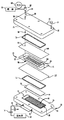
図7に示すように、底部シール層は、切り出し工程の後に超小形電子集成体とともに残留する金属プレート112’のような熱伝導性のシートまたはプレートを含むことができる。集成体の底面、即ち、チップ100’の後面106’は、例えば、シリコーン−シリカ組成物あるいは金属充填エポキシ(図示せず)のような伝熱性ダイ取着接着剤を使用して、伝熱シール層112’に結合される。接着剤は、カバー層の被着前は、シール層にまたはチップの表面に被着することができる。更に、各集成体104’は、チップ100’を包囲するリング101即ち支持構造体を有している。順応性のあるパッド即ち多孔質層98’は、チップと誘電層即ちテープ86’との間に配設されるとともに、リングとテープとの間にも配設される。かくして、チップと誘電層との間で封入材により形成される順応性のある層はまた、リングと誘電層との間を延びている。封入後は、切り出し工程は、各チップを、連係するリングとチップ及びリングを覆うテープの部分とともに残すように行われる。テープのこの一層大きい部分が、ファンアウト構造体またはファンイン/ファンアウト構造体と同様に、別の端子用の空間を提供する。リングは、シリコンまたはモリブデンのような比較適合性のある材料あるいは剛性ポリマから形成することができるとともに、電気的に不活性とすることができる。あるいは、リングは、コンデンサ、抵抗あるいは別の半導体素子のような1つ以上の電気構成素子を含むことができる。
Claims (58)
- 互いに逆を向く上面と底面とを有する複数の超小形電子集成体を封入する方法であって、(a)上面及び底面を有するフレームの開口内に前記集成体を配設するとともに、フレームの開口を介して延びるようにフレームに封止接続され、前記集成体を含む閉鎖空間を画成する上部及び底部シール層を配設する工程と、(b)上部取り付け具要素と底部取り付け具要素との間にフレーム、シール層及び集成体を係合させる工程と、(c)フレーム、シール層及び集成体が上部取り付け具要素と底部取り付け具要素との間に係合している状態でシール層の間及び集成体の周囲に液体封入材を注入する工程とを備え、前記シール層とフレームは液体封入材を含み、更に(d)液体封入材を硬化する工程を備えることを特徴とする方法。
- 集成体をフレームから取り出す工程を更に備えることを特徴とする請求項1に記載の方法。
- フレームは集成体をフレームから取り出すときに破壊されることを特徴とする請求項2に記載の方法。
- 新しいフレームと集成体を各繰り返しごとに使用して前記工程を繰り返す工程を更に備えることを特徴とする請求項3に記載の方法。
- 前記硬化工程の前に前記フレーム、シール層及び集成体を取り付け具から取り出す工程を更に備え、前記シール層及びフレームは前記硬化工程において前記封入材を保持することを特徴とする請求項1に記載の方法。
- 前記硬化工程は高温で行われることを特徴とする請求項5に記載の方法。
- 前記フレームは重合材料、繊維材料及びこれらの組み合わせよりなる群から選ばれる材料から形成されることを特徴とする請求項6に記載の方法。
- 前記封入材を注入する工程に先だって前記集成体の周囲及び前記シール層の間の空間を排気する工程を更に備えることを特徴とする請求項1に記載の方法。
- 前記注入工程は、前記シール層のうちの1つのシール層の孔を介して中空のニードルを前進させることにより前記ニードルを前記シール層間の前記閉鎖空間と連通させるとともに、封入材を前記中空ニードルを介して前記閉鎖空間に導く工程を含むことを特徴とする請求項8に記載の方法。
- 前記排気工程は真空を前記孔を介して印加することにより行われることを特徴とする請求項9に記載の方法。
- 前記孔を介して真空を印加する前記工程は前記ニードルが前記孔にないときに前記孔と連通する前記取り付け具要素のうちの1つの取り付け具要素の通路に真空を印加することにより行うことを特徴とする請求項10に記載の方法。
- シール層と前記取り付け具要素の前記1つとの間に前記孔を包囲する弾性ガスケットを押し込むことにより前記孔を有するシール層に前記取り付け具要素の前記1つをシールする工程を更に備えることを特徴とする請求項11に記載の方法。
- 前記フレームは前記孔を有するシール層を前記孔に近接して支持することを特徴とする請求項12に記載の方法。
- ニードルを前進させる前記工程は前記取り付け具要素のうちの前記1つの取り付け具要素の前記通路を介してニードルを前進させることにより行うことを特徴とする請求項11に記載の方法。
- 前記シール層は封入材を前記中空ニードルを介して空間に通す前記工程の際に前記孔においてニードルと封止係合することを特徴とする請求項14に記載の方法。
- 前記集成体は多孔質領域を有し、前記封入材は前記注入工程において前記多孔質領域に浸透することを特徴とする請求項1に記載の方法。
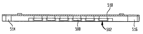
- 前記集成体、フレーム及びシール層を配設する前記工程は複数の半導体チップを一体テープに取着するとともに、それぞれが1つ以上の前記チップと連係するテープの領域とを有する複数の半導体チップ集成体を得るように前記テープの表面に露出した端子に前記チップを電気的に接続する工程と含むことを特徴とする請求項1に記載の方法。
- 前記集成体、フレーム及びシール層を配設する前記工程は前記テープとは別体をなすカバー層を配設するとともに、前記テープとカバー層とが協働して前記1つの前記シール層を構成するように該カバー層を前記テープの前記面に被着する工程を含むことを特徴とする請求項17に記載の方法。
- 前記シール層は前記テープを含み、前記集成体、フレーム及びシール層を配設する前記工程はテープをフレームに対してシールする工程を含むことを特徴とする請求項17に記載の方法。
- チップをテープに取着する前記工程は前記接点を担持する前記チップの前面が前記テープの方を向くように行われ、前記テープは前記集成体の上面を形成することを特徴とする請求項17に記載の方法。
- 前記集成体、フレーム及びシール層を配設する工程は前記底部シール層を前記チップの後面に被着する工程を含むことを特徴とする請求項20に記載の方法。
- 前記集成体、フレーム及びシール層を配設する前記工程は、前記封入材が前記封入材を注入する前記工程の際に前記チップの後面を覆うように前記チップの後面から離隔して底部シール層を被着することを特徴とする請求項20に記載の方法。
- チップをテープに取着する前記工程は、前記接点を担持する前記チップの前記前面が前記チップから離れた方を向くとともにチップの後面がテープの方を向くように行われ、前記テープは前記集成体の底面を形成し、前記上部シール層は前記チップの前記前面を覆うことを特徴とする請求項17に記載の方法。
- 前記上部シール層は、前記封入材が前記封入材を注入する前記工程の際に前記チップの前記前面と前記上部シール層との間を流れるように前記チップの前記前面の上方へ離隔していることを特徴とする請求項23に記載の方法。
- 前記チップは波長帯域の光と相互作用を行う光学活性素子を含み、前記上部シール層はかかる波長帯域の光に透明であり、前記方法は前記上部シール層の一部が前記各集成体とともに残るように前記集成体を前記フレームから取り出す工程を更に備えることを特徴とする請求項23に記載の方法。
- 前記上部シール層は前記波長帯域の光を屈折させる屈折素子を含むことを特徴とする請求項25に記載の方法。
- 前記上部シール層は熱伝導性であり、前記方法は前記上部シール層の一部が前記各集成体とともに残るように前記集成体を前記フレームから取り出す工程を更に備えることを特徴とする請求項23に記載の方法。
- 前記チップを取着しかつ前記チップを電気的に接続する前記工程は前記テープが前記フレームに取着されている状態で行われることを特徴とする請求項17に記載の方法。
- 前記チップと前記テープとの間に多孔質構造体を配設する工程を更に備え、前記封入材は前記注入工程の際に前記多孔質構造体を充填することを特徴とする請求項28に記載の方法。
- 前記多孔質構造体を配設する前記工程は前記テープが前記フレームに取着されている状態で柔軟性のあるパッドを前記テープに被着する工程を含むことを特徴とする請求項29に記載の方法。
- 前記テープは内部に開口を有し、前記チップを前記端子に電気的に接続する前記工程は前記開口を介して操作を行う工程を含み、前記上部シール層は前記開口をシールすることを特徴とする請求項28に記載の方法。
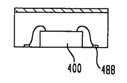
- 前記集成体、フレーム及びシール層を配設する前記工程は、複数の垂直方向に延びる壁が内部に形成されている底部シール層に複数の半導体チップを取着し、かつ、前記チップが配置されるポケットを画成する工程を含み、前記壁はチップの保護パッケージとして作用するように方法の終了後に各チップを少なくとも一部包囲することを特徴とする請求項1に記載の方法。
- フレーム、シール層及び集成体を取り付け具の上部要素と底部要素との間に係合させる前記工程は、取り付け具の上部要素とフレームを覆う上部シール層の部分との間に弾性のある上部ガスケットを押し込めとともに取り付け具の底部要素とフレームを覆う底部シール層の部分との間に弾性のある底部ガスケットを押し込める工程を含むことを特徴とする請求項1に記載の方法。
- 前記要素の一方にある浮動プレートを前記要素の他方に向けて付勢することにより、前記集成体と該集成体を覆うフレームの孔内にあるシール層の領域とを、浮動プレートと前記要素の前記他方の要素との間に押し込める工程を更に備えることを特徴とする請求項1に記載の方法。
- 前記浮動プレートを前記要素の他方へ向けて付勢する前記工程は封入材を注入する工程の際に行われることを特徴とする請求項34に記載の方法。
- 一方の前記シール層は金属材料から形成され、金属シール層の一部は超小形電子集成体の封入プロセス終了後に前記各集成体に取着保持されることによりシール層の前記部分が完成された集成体の熱伝導要素として作用することを特徴とする請求項1に記載の方法。
- 複数の半導体チップ集成体を製造する方法であって、 (a)複数の半導体チップを一体テープの底面に取着しかつテープがフレームに保持された状態で前記テープの上面に露出した端子に前記チップを電気的に接続することにより複数の半導体チップ集成体を提供する工程を備え、各半導体チップ集成体は1つ以上の前記チップと該チップと連係するテープの領域とを有し、前記チップは前記フレームにより取り囲まれる孔に配置され、更に(b)前記テープの前記上面及びフレームの上面に上部シール層を被着する工程と、 (c)前記テープから離れた方を向く前記チップの底面及び前記フレームの底面に底部シール層を被着する工程と、 (d)液体封入材がチップ及びテープと接触するように該封入材を前記チップの周囲に注入する工程と、 (e)封入材を硬化させる工程とを備え、前記フレームと前記シール層は前記硬化工程の際に前記封入材を保持するとともに前記封入材がチップの底面及びテープの上面と接触するのを防止する工程とを備えることを特徴とする方法。
- 前記注入工程に先立ち前記チップの周囲の前記シール層間のスペースを排気する工程を更に備えることを特徴とする請求項37に記載の方法。
- 構造体を備え、該構造体は上面及び底面と、前記上面から前記底面まで構造体を透通する孔とを有し、前記構造体は更に前記上面から構造体の中へ延びるニードル整合孔及び前記ニードル孔と前記孔との間を延びるゲートチャンネルを画成することを特徴とする封入フレーム。
- 前記ゲートチャンネルは前記上面に臨んでいることを特徴とする請求項39に記載の封入フレーム。
- 前記構造体は重合材料、繊維材料及びこれらの組み合わせよりなる群から選ばれる材料から形成されることを特徴とする請求項39に記載の封入フレーム。
- 前記構造体は紙及びフェノール樹脂よりなる群から選ばれる材料から形成されることを特徴とする請求項41に記載の封入フレーム。
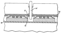
- (a)上部要素面、該上部要素面に臨む通路及び該通路と連通する真空接続体を有する上部取り付け具要素と、(b)先端部を有し、該先端部は該先端部が通路内にある退却位置と前記先端部が前記上部要素面を越えて突出する前進位置との間を動くように前記通路内に摺動自在に取着されている中空ニードルと、(c)該中空ニードルに接続された封入材ディスペンサと、 (d)上部要素面の方を向く底部要素面を有する底部取り付け具要素と、 (e)取り付け具要素と係合自在であり、かつ、取り付け具要素を互いに向けて付勢するように配設されたクランプとを備えることを特徴とする封入取り付け具。
- 前記上部取り付け具要素に取着され、かつ、前記上部要素面において前記通路を囲む先端O−リングを更に備えることを特徴とする請求項43に記載の取り付け具。
- 前記上部取り付け具要素に取着され、かつ、前記上部要素面から離隔して通路を囲む基端部O−リングを更に備え、前記真空接続体は前記O−リング間で前記通路と連通することを特徴とする請求項43に記載の取り付け具。
- 前記先端部O−リングは前記要素間に係合されるシール層及びフレーム集成体と封止係合するように前記上部要素面から突出することを特徴とする請求項43に記載の取り付け具。
- 前記取り付け具要素は前記面と平衡する水平方向に前記取り付け具要素を互いに対して位置決めする相互に係合自在の構成を有することを特徴とする請求項43に記載の取り付け具。
- 前記取り付け具要素の少なくとも1つは、フレームが取り付け具要素間に係合されているときにフレームと係合して該フレームを前記水平方向に配置するよう前記要素の面から突出する位置決め要素を有することを特徴とする請求項47に記載の取り付け具。
- (a)上部要素面を有する上部取り付け具要素と、 (b)中央領域及び該中央領域を包囲する周辺領域を有する底部取り付け具要素とを備え、前記周辺領域は上部要素面の方を向く底部要素面を有し、前記底部取り付け具要素は前記底部要素面に臨む前記中央領域に凹部を画成し、更に(c)底部取り付け具に対して上下に動くように前記底部取り付け具の前記凹部に取着された浮動プレートと、(d)取り付け具要素と係合自在であり、かつ、取り付け具要素を互いに向けて付勢するように配設されたクランプとを備え、取り付け具要素は底部プレートの中央領域及び浮動プレートと整合する孔内でフレーム担持超小形電子集成体と係合することができ、更に(e)孔内の超小形電子素子と係合しかつ上部プレートと係合するように超小形電子集成体を上方へ付勢するように前記浮動プレートを上部取り付け具要素へ向けて上方へ付勢する手段を備えることを特徴とする封入取り付け具。
- 前記付勢手段は前記凹部と連通する流体圧接続体を含むことを特徴とする請求項49に記載の取り付け具。
- 封入材ディスペンサを更に備えることを特徴とする請求項50に記載の取り付け具。
- (a)上面、底面及びこれらの面間を延びる孔をそれぞれ有する複数のフレームと、(b)上部及び底部取り付け具要素と、取り付け具要素を互いに向けて付勢するように配設されたクランプと、封入材ディスペンサとを有する取り付け具を備え、前記上部及び底部取り付け具要素は該要素間で前記フレームと連続して交互に係合するようになっており、前記封入材ディスペンサはフレームが取り付け具要素間に係合している状態で各フレームの孔に封入材を注入することを特徴とする封入装置。
- 前記封入材の注入後にフレームを保持するように取り付け具とは別体をなす硬化ステーションを更に備えることを特徴とする請求項52に記載の封入装置。
- 前記取り付け具は、フレームに封入材を充填する前に取り付け具要素間に係合する各フレームの孔に真空を印加する真空装置を有することを特徴とする請求項52に記載の封入装置。
- (a)上面及び底面と、該面間を延びる孔とを有するフレームと、(b)該フレームに封止接続され、前記フレームと協働して閉鎖空間を画成する上部及び底部シール層と、(c)前記閉鎖空間に配置された複数の超小形電子集成体とを備えることを特徴とする装置。
- 前記シール層の一方は一体テープを有し、前記各超小形電子集成体は前記テープの領域を含むことを特徴とする請求項55に記載の装置。
- 前記フレームは重合材料、繊維材料及びこれらの組み合わせよりなる群から選ばれる材料から形成されることを特徴とする請求項55に記載の装置。
- 未硬化の封入材を更に備え、前記シール層と前記フレームは協働して前記封入材を保持することを特徴とする請求項55に記載の装置。
Applications Claiming Priority (2)
| Application Number | Priority Date | Filing Date | Title |
|---|---|---|---|
| US09/067,698 | 1998-04-28 | ||
| US09/067,698 US6329224B1 (en) | 1998-04-28 | 1998-04-28 | Encapsulation of microelectronic assemblies |
Related Parent Applications (1)
| Application Number | Title | Priority Date | Filing Date |
|---|---|---|---|
| JP2000546394A Division JP4567189B2 (ja) | 1998-04-28 | 1999-04-26 | 超小形電子集成体を封入する方法、並びに、該方法で使用するための封入フレーム、封入取り付け具及び封入装置 |
Publications (2)
| Publication Number | Publication Date |
|---|---|
| JP2010004062A true JP2010004062A (ja) | 2010-01-07 |
| JP5345472B2 JP5345472B2 (ja) | 2013-11-20 |
Family
ID=22077773
Family Applications (2)
| Application Number | Title | Priority Date | Filing Date |
|---|---|---|---|
| JP2000546394A Expired - Lifetime JP4567189B2 (ja) | 1998-04-28 | 1999-04-26 | 超小形電子集成体を封入する方法、並びに、該方法で使用するための封入フレーム、封入取り付け具及び封入装置 |
| JP2009188707A Expired - Lifetime JP5345472B2 (ja) | 1998-04-28 | 2009-08-17 | 超小形電子集成体の封入 |
Family Applications Before (1)
| Application Number | Title | Priority Date | Filing Date |
|---|---|---|---|
| JP2000546394A Expired - Lifetime JP4567189B2 (ja) | 1998-04-28 | 1999-04-26 | 超小形電子集成体を封入する方法、並びに、該方法で使用するための封入フレーム、封入取り付け具及び封入装置 |
Country Status (5)
| Country | Link |
|---|---|
| US (2) | US6329224B1 (ja) |
| JP (2) | JP4567189B2 (ja) |
| KR (1) | KR100602462B1 (ja) |
| TW (1) | TW460988B (ja) |
| WO (1) | WO1999056316A1 (ja) |
Families Citing this family (182)
| Publication number | Priority date | Publication date | Assignee | Title |
|---|---|---|---|---|
| US7005326B1 (en) | 1998-06-24 | 2006-02-28 | Amkor Technology, Inc. | Method of making an integrated circuit package |
| US7112474B1 (en) | 1998-06-24 | 2006-09-26 | Amkor Technology, Inc. | Method of making an integrated circuit package |
| US7030474B1 (en) | 1998-06-24 | 2006-04-18 | Amkor Technology, Inc. | Plastic integrated circuit package and method and leadframe for making the package |
| US7071541B1 (en) | 1998-06-24 | 2006-07-04 | Amkor Technology, Inc. | Plastic integrated circuit package and method and leadframe for making the package |
| US7332375B1 (en) | 1998-06-24 | 2008-02-19 | Amkor Technology, Inc. | Method of making an integrated circuit package |
| US6143981A (en) | 1998-06-24 | 2000-11-07 | Amkor Technology, Inc. | Plastic integrated circuit package and method and leadframe for making the package |
| US6893900B1 (en) | 1998-06-24 | 2005-05-17 | Amkor Technology, Inc. | Method of making an integrated circuit package |
| US6448633B1 (en) | 1998-11-20 | 2002-09-10 | Amkor Technology, Inc. | Semiconductor package and method of making using leadframe having lead locks to secure leads to encapsulant |
| JP3653417B2 (ja) * | 1999-06-09 | 2005-05-25 | 株式会社日立製作所 | マルチチップモジュールの封止構造 |
| JP3417879B2 (ja) * | 1999-07-05 | 2003-06-16 | 沖電気工業株式会社 | モールド金型 |
| KR100379089B1 (ko) | 1999-10-15 | 2003-04-08 | 앰코 테크놀로지 코리아 주식회사 | 리드프레임 및 이를 이용한 반도체패키지 |
| KR20010037247A (ko) | 1999-10-15 | 2001-05-07 | 마이클 디. 오브라이언 | 반도체패키지 |
| KR100403142B1 (ko) | 1999-10-15 | 2003-10-30 | 앰코 테크놀로지 코리아 주식회사 | 반도체패키지 |
| US6580159B1 (en) | 1999-11-05 | 2003-06-17 | Amkor Technology, Inc. | Integrated circuit device packages and substrates for making the packages |
| US6847103B1 (en) | 1999-11-09 | 2005-01-25 | Amkor Technology, Inc. | Semiconductor package with exposed die pad and body-locking leadframe |
| US6602740B1 (en) * | 1999-11-24 | 2003-08-05 | Tessera, Inc. | Encapsulation of microelectronic assemblies |
| KR100421774B1 (ko) | 1999-12-16 | 2004-03-10 | 앰코 테크놀로지 코리아 주식회사 | 반도체패키지 및 그 제조 방법 |
| US6444035B1 (en) | 2000-01-28 | 2002-09-03 | Speedline Technologies, Inc. | Conveyorized vacuum injection system |
| US6644238B2 (en) | 2000-01-28 | 2003-11-11 | Speedline Technologies, Inc. | Conveyorized vacuum injection system |
| DE10006738C2 (de) * | 2000-02-15 | 2002-01-17 | Osram Opto Semiconductors Gmbh | Lichtemittierendes Bauelement mit verbesserter Lichtauskopplung und Verfahren zu seiner Herstellung |
| US7205578B2 (en) * | 2000-02-15 | 2007-04-17 | Osram Gmbh | Semiconductor component which emits radiation, and method for producing the same |
| KR100583494B1 (ko) | 2000-03-25 | 2006-05-24 | 앰코 테크놀로지 코리아 주식회사 | 반도체패키지 |
| KR100559664B1 (ko) * | 2000-03-25 | 2006-03-10 | 앰코 테크놀로지 코리아 주식회사 | 반도체패키지 |
| US7042068B2 (en) | 2000-04-27 | 2006-05-09 | Amkor Technology, Inc. | Leadframe and semiconductor package made using the leadframe |
| DE20111659U1 (de) * | 2000-05-23 | 2001-12-13 | OSRAM Opto Semiconductors GmbH & Co. oHG, 93049 Regensburg | Bauelement für die Optoelektronik |
| US20020020898A1 (en) | 2000-08-16 | 2002-02-21 | Vu Quat T. | Microelectronic substrates with integrated devices |
| KR20020058209A (ko) | 2000-12-29 | 2002-07-12 | 마이클 디. 오브라이언 | 반도체패키지 |
| US6967395B1 (en) | 2001-03-20 | 2005-11-22 | Amkor Technology, Inc. | Mounting for a package containing a chip |
| US6706553B2 (en) | 2001-03-26 | 2004-03-16 | Intel Corporation | Dispensing process for fabrication of microelectronic packages |
| KR100369393B1 (ko) | 2001-03-27 | 2003-02-05 | 앰코 테크놀로지 코리아 주식회사 | 리드프레임 및 이를 이용한 반도체패키지와 그 제조 방법 |
| KR100393448B1 (ko) | 2001-03-27 | 2003-08-02 | 앰코 테크놀로지 코리아 주식회사 | 반도체 패키지 및 그 제조 방법 |
| US7498196B2 (en) | 2001-03-30 | 2009-03-03 | Megica Corporation | Structure and manufacturing method of chip scale package |
| US7064009B1 (en) | 2001-04-04 | 2006-06-20 | Amkor Technology, Inc. | Thermally enhanced chip scale lead on chip semiconductor package and method of making same |
| US6597059B1 (en) | 2001-04-04 | 2003-07-22 | Amkor Technology, Inc. | Thermally enhanced chip scale lead on chip semiconductor package |
| US7045883B1 (en) | 2001-04-04 | 2006-05-16 | Amkor Technology, Inc. | Thermally enhanced chip scale lead on chip semiconductor package and method of making same |
| US6601753B2 (en) * | 2001-05-17 | 2003-08-05 | Visteon Global Technologies, Inc. | Void-free die attachment method with low melting metal |
| DE10133151B4 (de) * | 2001-07-07 | 2004-07-29 | Robert Bosch Gmbh | Bauteil mit einem Gehäuse umgebenen Bauelement und Vorrichtung und Verfahren, die bei seiner Herstellung einsetzbar sind |
| US6555486B2 (en) * | 2001-07-12 | 2003-04-29 | Cool Shield, Inc. | Thermally conductive silk-screenable interface material |
| US7485952B1 (en) | 2001-09-19 | 2009-02-03 | Amkor Technology, Inc. | Drop resistant bumpers for fully molded memory cards |
| US6900527B1 (en) | 2001-09-19 | 2005-05-31 | Amkor Technology, Inc. | Lead-frame method and assembly for interconnecting circuits within a circuit module |
| US6608391B1 (en) * | 2001-12-19 | 2003-08-19 | Orient Semiconductor Electronics Limited | Preparation method of underfill for flip chip package and the device |
| TW584950B (en) | 2001-12-31 | 2004-04-21 | Megic Corp | Chip packaging structure and process thereof |
| TW544882B (en) | 2001-12-31 | 2003-08-01 | Megic Corp | Chip package structure and process thereof |
| US6673698B1 (en) * | 2002-01-19 | 2004-01-06 | Megic Corporation | Thin film semiconductor package utilizing a glass substrate with composite polymer/metal interconnect layers |
| TW517361B (en) | 2001-12-31 | 2003-01-11 | Megic Corp | Chip package structure and its manufacture process |
| TW503496B (en) | 2001-12-31 | 2002-09-21 | Megic Corp | Chip packaging structure and manufacturing process of the same |
| US7723162B2 (en) * | 2002-03-22 | 2010-05-25 | White Electronic Designs Corporation | Method for producing shock and tamper resistant microelectronic devices |
| US6608366B1 (en) | 2002-04-15 | 2003-08-19 | Harry J. Fogelson | Lead frame with plated end leads |
| US6984545B2 (en) * | 2002-07-22 | 2006-01-10 | Micron Technology, Inc. | Methods of encapsulating selected locations of a semiconductor die assembly using a thick solder mask |
| US6818973B1 (en) | 2002-09-09 | 2004-11-16 | Amkor Technology, Inc. | Exposed lead QFP package fabricated through the use of a partial saw process |
| US6919620B1 (en) | 2002-09-17 | 2005-07-19 | Amkor Technology, Inc. | Compact flash memory card with clamshell leadframe |
| US7265045B2 (en) * | 2002-10-24 | 2007-09-04 | Megica Corporation | Method for fabricating thermal compliant semiconductor chip wiring structure for chip scale packaging |
| US7190062B1 (en) | 2004-06-15 | 2007-03-13 | Amkor Technology, Inc. | Embedded leadframe semiconductor package |
| US7361533B1 (en) | 2002-11-08 | 2008-04-22 | Amkor Technology, Inc. | Stacked embedded leadframe |
| US6905914B1 (en) | 2002-11-08 | 2005-06-14 | Amkor Technology, Inc. | Wafer level package and fabrication method |
| US6847099B1 (en) | 2003-02-05 | 2005-01-25 | Amkor Technology Inc. | Offset etched corner leads for semiconductor package |
| US6879028B2 (en) * | 2003-02-21 | 2005-04-12 | Freescale Semiconductor, Inc. | Multi-die semiconductor package |
| US6927483B1 (en) | 2003-03-07 | 2005-08-09 | Amkor Technology, Inc. | Semiconductor package exhibiting efficient lead placement |
| US6815254B2 (en) * | 2003-03-10 | 2004-11-09 | Freescale Semiconductor, Inc. | Semiconductor package with multiple sides having package contacts |
| US7001799B1 (en) | 2003-03-13 | 2006-02-21 | Amkor Technology, Inc. | Method of making a leadframe for semiconductor devices |
| US6794740B1 (en) | 2003-03-13 | 2004-09-21 | Amkor Technology, Inc. | Leadframe package for semiconductor devices |
| US7095103B1 (en) | 2003-05-01 | 2006-08-22 | Amkor Technology, Inc. | Leadframe based memory card |
| US6879034B1 (en) | 2003-05-01 | 2005-04-12 | Amkor Technology, Inc. | Semiconductor package including low temperature co-fired ceramic substrate |
| US7008825B1 (en) | 2003-05-27 | 2006-03-07 | Amkor Technology, Inc. | Leadframe strip having enhanced testability |
| US6897550B1 (en) | 2003-06-11 | 2005-05-24 | Amkor Technology, Inc. | Fully-molded leadframe stand-off feature |
| FR2856517B1 (fr) * | 2003-06-17 | 2005-09-23 | St Microelectronics Sa | Procede de fabrication de composant semi-conducteur et composant semi-conducteur |
| US7245007B1 (en) | 2003-09-18 | 2007-07-17 | Amkor Technology, Inc. | Exposed lead interposer leadframe package |
| US7915085B2 (en) * | 2003-09-18 | 2011-03-29 | Cree, Inc. | Molded chip fabrication method |
| US6921967B2 (en) | 2003-09-24 | 2005-07-26 | Amkor Technology, Inc. | Reinforced die pad support structure |
| US7138707B1 (en) | 2003-10-21 | 2006-11-21 | Amkor Technology, Inc. | Semiconductor package including leads and conductive posts for providing increased functionality |
| US7144517B1 (en) | 2003-11-07 | 2006-12-05 | Amkor Technology, Inc. | Manufacturing method for leadframe and for semiconductor package using the leadframe |
| US7211879B1 (en) | 2003-11-12 | 2007-05-01 | Amkor Technology, Inc. | Semiconductor package with chamfered corners and method of manufacturing the same |
| US7087465B2 (en) * | 2003-12-15 | 2006-08-08 | Philips Lumileds Lighting Company, Llc | Method of packaging a semiconductor light emitting device |
| KR100572207B1 (ko) * | 2003-12-18 | 2006-04-19 | 주식회사 디지탈바이오테크놀러지 | 플라스틱 마이크로 칩의 접합 방법 |
| US7057268B1 (en) | 2004-01-27 | 2006-06-06 | Amkor Technology, Inc. | Cavity case with clip/plug for use on multi-media card |
| US7091594B1 (en) | 2004-01-28 | 2006-08-15 | Amkor Technology, Inc. | Leadframe type semiconductor package having reduced inductance and its manufacturing method |
| US6970360B2 (en) * | 2004-03-18 | 2005-11-29 | International Business Machines Corporation | Tamper-proof enclosure for a circuit card |
| US7153462B2 (en) * | 2004-04-23 | 2006-12-26 | Vishay Infrared Components, Inc. | Injection casting system for encapsulating semiconductor devices and method of use |
| US20050242425A1 (en) * | 2004-04-30 | 2005-11-03 | Leal George R | Semiconductor device with a protected active die region and method therefor |
| US7202554B1 (en) | 2004-08-19 | 2007-04-10 | Amkor Technology, Inc. | Semiconductor package and its manufacturing method |
| US7217583B2 (en) * | 2004-09-21 | 2007-05-15 | Cree, Inc. | Methods of coating semiconductor light emitting elements by evaporating solvent from a suspension |
| US7217991B1 (en) | 2004-10-22 | 2007-05-15 | Amkor Technology, Inc. | Fan-in leadframe semiconductor package |
| CN101053079A (zh) | 2004-11-03 | 2007-10-10 | 德塞拉股份有限公司 | 堆叠式封装的改进 |
| US7288847B2 (en) * | 2005-01-25 | 2007-10-30 | Medtronic, Inc. | Assembly including a circuit and an encapsulation frame, and method of making the same |
| US7160798B2 (en) * | 2005-02-24 | 2007-01-09 | Freescale Semiconductor, Inc. | Method of making reinforced semiconductor package |
| JP4588506B2 (ja) * | 2005-03-25 | 2010-12-01 | 大日本印刷株式会社 | 塗布液の塗布装置および塗布方法 |
| US20070096345A1 (en) * | 2005-11-03 | 2007-05-03 | Vishay Vitramon Inc. | Frame packaged array electronic component |
| US7507603B1 (en) | 2005-12-02 | 2009-03-24 | Amkor Technology, Inc. | Etch singulated semiconductor package |
| US7572681B1 (en) | 2005-12-08 | 2009-08-11 | Amkor Technology, Inc. | Embedded electronic component package |
| US8337071B2 (en) | 2005-12-21 | 2012-12-25 | Cree, Inc. | Lighting device |
| US8058101B2 (en) | 2005-12-23 | 2011-11-15 | Tessera, Inc. | Microelectronic packages and methods therefor |
| US8969908B2 (en) | 2006-04-04 | 2015-03-03 | Cree, Inc. | Uniform emission LED package |
| US7943952B2 (en) * | 2006-07-31 | 2011-05-17 | Cree, Inc. | Method of uniform phosphor chip coating and LED package fabricated using method |
| US7569422B2 (en) | 2006-08-11 | 2009-08-04 | Megica Corporation | Chip package and method for fabricating the same |
| US10295147B2 (en) | 2006-11-09 | 2019-05-21 | Cree, Inc. | LED array and method for fabricating same |
| US9024349B2 (en) | 2007-01-22 | 2015-05-05 | Cree, Inc. | Wafer level phosphor coating method and devices fabricated utilizing method |
| US8232564B2 (en) * | 2007-01-22 | 2012-07-31 | Cree, Inc. | Wafer level phosphor coating technique for warm light emitting diodes |
| US9159888B2 (en) | 2007-01-22 | 2015-10-13 | Cree, Inc. | Wafer level phosphor coating method and devices fabricated utilizing method |
| US7776746B2 (en) * | 2007-02-28 | 2010-08-17 | Alpha And Omega Semiconductor Incorporated | Method and apparatus for ultra thin wafer backside processing |
| KR101391925B1 (ko) * | 2007-02-28 | 2014-05-07 | 페어차일드코리아반도체 주식회사 | 반도체 패키지 및 이를 제조하기 위한 반도체 패키지 금형 |
| US20080251908A1 (en) * | 2007-04-11 | 2008-10-16 | Advanced Chip Engineering Technology Inc. | Semiconductor device package having multi-chips with side-by-side configuration and method of the same |
| US20080265402A1 (en) * | 2007-04-30 | 2008-10-30 | International Business Machines Corporation | Rework process and method for lead-free capped multi-core modules with organic substrates |
| US10505083B2 (en) | 2007-07-11 | 2019-12-10 | Cree, Inc. | Coating method utilizing phosphor containment structure and devices fabricated using same |
| US7687899B1 (en) | 2007-08-07 | 2010-03-30 | Amkor Technology, Inc. | Dual laminate package structure with embedded elements |
| US9041285B2 (en) | 2007-12-14 | 2015-05-26 | Cree, Inc. | Phosphor distribution in LED lamps using centrifugal force |
| US8167674B2 (en) * | 2007-12-14 | 2012-05-01 | Cree, Inc. | Phosphor distribution in LED lamps using centrifugal force |
| US8878219B2 (en) * | 2008-01-11 | 2014-11-04 | Cree, Inc. | Flip-chip phosphor coating method and devices fabricated utilizing method |
| US7723852B1 (en) | 2008-01-21 | 2010-05-25 | Amkor Technology, Inc. | Stacked semiconductor package and method of making same |
| CN101241874B (zh) * | 2008-02-21 | 2010-09-15 | 日月光半导体制造股份有限公司 | 封装设备及其基板载具 |
| US8637883B2 (en) | 2008-03-19 | 2014-01-28 | Cree, Inc. | Low index spacer layer in LED devices |
| US8240875B2 (en) | 2008-06-25 | 2012-08-14 | Cree, Inc. | Solid state linear array modules for general illumination |
| US7971347B2 (en) * | 2008-06-27 | 2011-07-05 | Intel Corporation | Method of interconnecting workpieces |
| US8072050B1 (en) | 2008-11-18 | 2011-12-06 | Amkor Technology, Inc. | Semiconductor device with increased I/O leadframe including passive device |
| US20170117214A1 (en) | 2009-01-05 | 2017-04-27 | Amkor Technology, Inc. | Semiconductor device with through-mold via |
| JP2011100718A (ja) * | 2009-10-05 | 2011-05-19 | Yazaki Corp | コネクタ |
| US8639373B2 (en) * | 2009-10-14 | 2014-01-28 | Stmicroelectronics, Inc. | Modular low stress package technology |
| US8937381B1 (en) | 2009-12-03 | 2015-01-20 | Amkor Technology, Inc. | Thin stackable package and method |
| US9691734B1 (en) | 2009-12-07 | 2017-06-27 | Amkor Technology, Inc. | Method of forming a plurality of electronic component packages |
| US8324511B1 (en) | 2010-04-06 | 2012-12-04 | Amkor Technology, Inc. | Through via nub reveal method and structure |
| US9159708B2 (en) | 2010-07-19 | 2015-10-13 | Tessera, Inc. | Stackable molded microelectronic packages with area array unit connectors |
| US8482111B2 (en) | 2010-07-19 | 2013-07-09 | Tessera, Inc. | Stackable molded microelectronic packages |
| US10546846B2 (en) | 2010-07-23 | 2020-01-28 | Cree, Inc. | Light transmission control for masking appearance of solid state light sources |
| US8440554B1 (en) | 2010-08-02 | 2013-05-14 | Amkor Technology, Inc. | Through via connected backside embedded circuit features structure and method |
| US8487445B1 (en) | 2010-10-05 | 2013-07-16 | Amkor Technology, Inc. | Semiconductor device having through electrodes protruding from dielectric layer |
| US9088226B2 (en) | 2010-10-19 | 2015-07-21 | Electronics Motion Systems Holding Limited | Power module for converting DC to AC |
| US8390130B1 (en) | 2011-01-06 | 2013-03-05 | Amkor Technology, Inc. | Through via recessed reveal structure and method |
| US8648450B1 (en) | 2011-01-27 | 2014-02-11 | Amkor Technology, Inc. | Semiconductor device including leadframe with a combination of leads and lands |
| TWI557183B (zh) | 2015-12-16 | 2016-11-11 | 財團法人工業技術研究院 | 矽氧烷組成物、以及包含其之光電裝置 |
| US9166126B2 (en) | 2011-01-31 | 2015-10-20 | Cree, Inc. | Conformally coated light emitting devices and methods for providing the same |
| KR101128063B1 (ko) | 2011-05-03 | 2012-04-23 | 테세라, 인코포레이티드 | 캡슐화 층의 표면에 와이어 본드를 구비하는 패키지 적층형 어셈블리 |
| EP2659172B1 (en) * | 2011-05-13 | 2019-06-26 | Siemens Healthcare Diagnostics Inc. | Rotary shear valve with tree-point stator seating |
| DE102011112476A1 (de) * | 2011-09-05 | 2013-03-07 | Epcos Ag | Bauelement und Verfahren zum Herstellen eines Bauelements |
| US8866278B1 (en) | 2011-10-10 | 2014-10-21 | Amkor Technology, Inc. | Semiconductor device with increased I/O configuration |
| US9105483B2 (en) | 2011-10-17 | 2015-08-11 | Invensas Corporation | Package-on-package assembly with wire bond vias |
| US8552548B1 (en) | 2011-11-29 | 2013-10-08 | Amkor Technology, Inc. | Conductive pad on protruding through electrode semiconductor device |
| US8946757B2 (en) | 2012-02-17 | 2015-02-03 | Invensas Corporation | Heat spreading substrate with embedded interconnects |
| US8372741B1 (en) | 2012-02-24 | 2013-02-12 | Invensas Corporation | Method for package-on-package assembly with wire bonds to encapsulation surface |
| US9704725B1 (en) | 2012-03-06 | 2017-07-11 | Amkor Technology, Inc. | Semiconductor device with leadframe configured to facilitate reduced burr formation |
| US9129943B1 (en) | 2012-03-29 | 2015-09-08 | Amkor Technology, Inc. | Embedded component package and fabrication method |
| US9048298B1 (en) | 2012-03-29 | 2015-06-02 | Amkor Technology, Inc. | Backside warpage control structure and fabrication method |
| US8835228B2 (en) | 2012-05-22 | 2014-09-16 | Invensas Corporation | Substrate-less stackable package with wire-bond interconnect |
| US9391008B2 (en) | 2012-07-31 | 2016-07-12 | Invensas Corporation | Reconstituted wafer-level package DRAM |
| US9502390B2 (en) | 2012-08-03 | 2016-11-22 | Invensas Corporation | BVA interposer |
| US8878353B2 (en) | 2012-12-20 | 2014-11-04 | Invensas Corporation | Structure for microelectronic packaging with bond elements to encapsulation surface |
| US9136254B2 (en) | 2013-02-01 | 2015-09-15 | Invensas Corporation | Microelectronic package having wire bond vias and stiffening layer |
| KR101486790B1 (ko) | 2013-05-02 | 2015-01-28 | 앰코 테크놀로지 코리아 주식회사 | 강성보강부를 갖는 마이크로 리드프레임 |
| US9167710B2 (en) | 2013-08-07 | 2015-10-20 | Invensas Corporation | Embedded packaging with preformed vias |
| US9685365B2 (en) | 2013-08-08 | 2017-06-20 | Invensas Corporation | Method of forming a wire bond having a free end |
| US20150076714A1 (en) | 2013-09-16 | 2015-03-19 | Invensas Corporation | Microelectronic element with bond elements to encapsulation surface |
| KR101563911B1 (ko) | 2013-10-24 | 2015-10-28 | 앰코 테크놀로지 코리아 주식회사 | 반도체 패키지 |
| US9379074B2 (en) | 2013-11-22 | 2016-06-28 | Invensas Corporation | Die stacks with one or more bond via arrays of wire bond wires and with one or more arrays of bump interconnects |
| US9263394B2 (en) | 2013-11-22 | 2016-02-16 | Invensas Corporation | Multiple bond via arrays of different wire heights on a same substrate |
| US9583456B2 (en) | 2013-11-22 | 2017-02-28 | Invensas Corporation | Multiple bond via arrays of different wire heights on a same substrate |
| US9583411B2 (en) | 2014-01-17 | 2017-02-28 | Invensas Corporation | Fine pitch BVA using reconstituted wafer with area array accessible for testing |
| US9673122B2 (en) | 2014-05-02 | 2017-06-06 | Amkor Technology, Inc. | Micro lead frame structure having reinforcing portions and method |
| US10381326B2 (en) | 2014-05-28 | 2019-08-13 | Invensas Corporation | Structure and method for integrated circuits packaging with increased density |
| US9412714B2 (en) | 2014-05-30 | 2016-08-09 | Invensas Corporation | Wire bond support structure and microelectronic package including wire bonds therefrom |
| CN104022145B (zh) * | 2014-06-23 | 2017-01-25 | 深圳市华星光电技术有限公司 | 基板的封装方法及封装结构 |
| US9484228B2 (en) * | 2014-10-01 | 2016-11-01 | Apple Inc. | Simultaneous independently controlled dual side PCB molding technique |
| US9735084B2 (en) | 2014-12-11 | 2017-08-15 | Invensas Corporation | Bond via array for thermal conductivity |
| US9888579B2 (en) | 2015-03-05 | 2018-02-06 | Invensas Corporation | Pressing of wire bond wire tips to provide bent-over tips |
| US9502372B1 (en) | 2015-04-30 | 2016-11-22 | Invensas Corporation | Wafer-level packaging using wire bond wires in place of a redistribution layer |
| US9761554B2 (en) | 2015-05-07 | 2017-09-12 | Invensas Corporation | Ball bonding metal wire bond wires to metal pads |
| US9683278B2 (en) * | 2015-06-08 | 2017-06-20 | Infineon Technologies Ag | Diffusion solder bonding using solder preforms |
| US10490528B2 (en) | 2015-10-12 | 2019-11-26 | Invensas Corporation | Embedded wire bond wires |
| US9490222B1 (en) | 2015-10-12 | 2016-11-08 | Invensas Corporation | Wire bond wires for interference shielding |
| US10332854B2 (en) | 2015-10-23 | 2019-06-25 | Invensas Corporation | Anchoring structure of fine pitch bva |
| US10181457B2 (en) | 2015-10-26 | 2019-01-15 | Invensas Corporation | Microelectronic package for wafer-level chip scale packaging with fan-out |
| US10043779B2 (en) | 2015-11-17 | 2018-08-07 | Invensas Corporation | Packaged microelectronic device for a package-on-package device |
| US9659848B1 (en) | 2015-11-18 | 2017-05-23 | Invensas Corporation | Stiffened wires for offset BVA |
| US9984992B2 (en) | 2015-12-30 | 2018-05-29 | Invensas Corporation | Embedded wire bond wires for vertical integration with separate surface mount and wire bond mounting surfaces |
| US9935075B2 (en) | 2016-07-29 | 2018-04-03 | Invensas Corporation | Wire bonding method and apparatus for electromagnetic interference shielding |
| US20180117813A1 (en) * | 2016-11-02 | 2018-05-03 | Asm Technology Singapore Pte Ltd | Molding apparatus including a compressible structure |
| US10299368B2 (en) | 2016-12-21 | 2019-05-21 | Invensas Corporation | Surface integrated waveguides and circuit structures therefor |
| DE102017131110B4 (de) * | 2017-12-22 | 2025-01-02 | OSRAM Opto Semiconductors Gesellschaft mit beschränkter Haftung | Verfahren und formwerkzeug zum einbetten von optoelektronischen bauelementen in eine schicht |
| DE102019132314B4 (de) * | 2019-11-28 | 2022-03-03 | Infineon Technologies Ag | Package mit Einkapselung unter Kompressionsbelastung |
| WO2022025160A1 (ja) * | 2020-07-31 | 2022-02-03 | ボンドテック株式会社 | チップ接合システムおよびチップ接合方法 |
| KR102484243B1 (ko) * | 2020-11-06 | 2023-01-04 | 양해춘 | 정밀 간격 배치용 포켓을 구비한 반도체 패키지의 마운팅 테이블 및 이 마운팅 테이블을 구비한 반도체 패키지 마운팅 시스템 |
| KR102569629B1 (ko) * | 2020-12-10 | 2023-08-22 | 봅스트 맥스 에스에이 | 평평한 가요성 부품을 유지하기 위한 포지셔닝 디바이스및 포지셔닝 조립체, 및 시트 재료 처리 기계 |
| USD1094325S1 (en) | 2021-08-24 | 2025-09-23 | Vishay Dale Electronics, Llc | Electro-magnetic device |
| CN116253577B (zh) | 2023-03-10 | 2024-03-29 | 合肥圣达电子科技实业有限公司 | 一种量子计算用陶瓷外壳及其制备方法 |
| CN119495607A (zh) * | 2024-11-12 | 2025-02-21 | 山东享视科技有限公司 | 一种芯片封装装置及封装方法 |
Citations (1)
| Publication number | Priority date | Publication date | Assignee | Title |
|---|---|---|---|---|
| WO1997011486A1 (en) * | 1995-09-22 | 1997-03-27 | Tessera, Inc. | Connecting multiple microelectronic elements with lead deformation |
Family Cites Families (26)
| Publication number | Priority date | Publication date | Assignee | Title |
|---|---|---|---|---|
| JPS5681957A (en) * | 1979-12-07 | 1981-07-04 | Hitachi Ltd | Semiconductor package using thermoplastic resin and manufacture thereof |
| JPS60193365A (ja) * | 1984-03-15 | 1985-10-01 | Nec Corp | リ−ドフレ−ム |
| JPS622592A (ja) * | 1985-06-28 | 1987-01-08 | 株式会社東芝 | 平滑型回路モジユ−ルの製造方法 |
| JPS62244139A (ja) * | 1986-04-17 | 1987-10-24 | Citizen Watch Co Ltd | 樹脂封止型ピングリツドアレイ及びその製造方法 |
| US4890383A (en) | 1988-01-15 | 1990-01-02 | Simens Corporate Research & Support, Inc. | Method for producing displays and modular components |
| JPH0225057A (ja) | 1988-07-13 | 1990-01-26 | Mitsubishi Electric Corp | 半導体装置の製造方法 |
| GB8911607D0 (en) * | 1989-05-19 | 1989-07-05 | Emi Plc Thorn | A method of encapsulation for electronic devices and devices so encapsulated |
| JPH03108745A (ja) * | 1989-09-22 | 1991-05-08 | Seiko Epson Corp | 半導体装置 |
| US4996170A (en) | 1990-07-30 | 1991-02-26 | Motorola, Inc. | Molding process for encapsulating semiconductor devices using a thixotropic compound |
| US5679977A (en) | 1990-09-24 | 1997-10-21 | Tessera, Inc. | Semiconductor chip assemblies, methods of making same and components for same |
| JPH04312965A (ja) * | 1991-03-29 | 1992-11-04 | Mitsubishi Electric Corp | メモリic |
| US5158912A (en) * | 1991-04-09 | 1992-10-27 | Digital Equipment Corporation | Integral heatsink semiconductor package |
| US5258650A (en) | 1991-08-26 | 1993-11-02 | Motorola, Inc. | Semiconductor device having encapsulation comprising of a thixotropic fluorosiloxane material |
| US5349234A (en) | 1992-05-29 | 1994-09-20 | Eastman Kodak Company | Package and method for assembly of infra-red imaging devices |
| US5468994A (en) | 1992-12-10 | 1995-11-21 | Hewlett-Packard Company | High pin count package for semiconductor device |
| US5369056A (en) | 1993-03-29 | 1994-11-29 | Staktek Corporation | Warp-resistent ultra-thin integrated circuit package fabrication method |
| US5477611A (en) * | 1993-09-20 | 1995-12-26 | Tessera, Inc. | Method of forming interface between die and chip carrier |
| US5518964A (en) | 1994-07-07 | 1996-05-21 | Tessera, Inc. | Microelectronic mounting with multiple lead deformation and bonding |
| US5554821A (en) * | 1994-07-15 | 1996-09-10 | National Semiconductor Corporation | Removable computer peripheral cards having a solid one-piece housing |
| US5659952A (en) | 1994-09-20 | 1997-08-26 | Tessera, Inc. | Method of fabricating compliant interface for semiconductor chip |
| US5607882A (en) * | 1994-12-20 | 1997-03-04 | Lucent Technologies Inc. | Multi-component electronic devices and methods for making them |
| US5766987A (en) * | 1995-09-22 | 1998-06-16 | Tessera, Inc. | Microelectronic encapsulation methods and equipment |
| US5765692A (en) * | 1995-11-13 | 1998-06-16 | Minnesota Mining And Manufacturing Company | Carrier tape with adhesive and protective walls |
| US5700723A (en) * | 1996-05-15 | 1997-12-23 | Lsi Logic Corporation | Method of packaging an integrated circuit |
| KR100251859B1 (ko) * | 1997-01-28 | 2000-04-15 | 마이클 디. 오브라이언 | 가요성 회로 기판 스트립을 이용하여 제조되는 볼그리드 어레이반도체 패키지의 싱귤레이션 방법 |
| US5923959A (en) * | 1997-07-23 | 1999-07-13 | Micron Technology, Inc. | Ball grid array (BGA) encapsulation mold |
-
1998
- 1998-04-28 US US09/067,698 patent/US6329224B1/en not_active Expired - Lifetime
-
1999
- 1999-04-26 WO PCT/US1999/009020 patent/WO1999056316A1/en not_active Ceased
- 1999-04-26 JP JP2000546394A patent/JP4567189B2/ja not_active Expired - Lifetime
- 1999-04-26 TW TW088106646A patent/TW460988B/zh not_active IP Right Cessation
- 1999-04-26 KR KR1020007012035A patent/KR100602462B1/ko not_active Expired - Lifetime
-
2001
- 2001-06-06 US US09/875,383 patent/US6541874B2/en not_active Expired - Lifetime
-
2009
- 2009-08-17 JP JP2009188707A patent/JP5345472B2/ja not_active Expired - Lifetime
Patent Citations (2)
| Publication number | Priority date | Publication date | Assignee | Title |
|---|---|---|---|---|
| WO1997011486A1 (en) * | 1995-09-22 | 1997-03-27 | Tessera, Inc. | Connecting multiple microelectronic elements with lead deformation |
| JPH11512875A (ja) * | 1995-09-22 | 1999-11-02 | テセラ,インコーポレイテッド | リード変形を有する接続多重超小形電子素子 |
Also Published As
| Publication number | Publication date |
|---|---|
| US6329224B1 (en) | 2001-12-11 |
| US20010023995A1 (en) | 2001-09-27 |
| JP4567189B2 (ja) | 2010-10-20 |
| JP5345472B2 (ja) | 2013-11-20 |
| TW460988B (en) | 2001-10-21 |
| WO1999056316A1 (en) | 1999-11-04 |
| US6541874B2 (en) | 2003-04-01 |
| KR100602462B1 (ko) | 2006-07-19 |
| JP2002513209A (ja) | 2002-05-08 |
| KR20010043140A (ko) | 2001-05-25 |
Similar Documents
| Publication | Publication Date | Title |
|---|---|---|
| JP4567189B2 (ja) | 超小形電子集成体を封入する方法、並びに、該方法で使用するための封入フレーム、封入取り付け具及び封入装置 | |
| US6602740B1 (en) | Encapsulation of microelectronic assemblies | |
| KR101162404B1 (ko) | 수지 밀봉 발광체 및 그 제조 방법 | |
| KR100384255B1 (ko) | 반도체칩용컴플리언트인터페이스 | |
| US6521480B1 (en) | Method for making a semiconductor chip package | |
| US6458628B1 (en) | Methods of encapsulating a semiconductor chip using a settable encapsulant | |
| US6503780B1 (en) | Wafer scale image sensor package fabrication method | |
| CN101261985B (zh) | 形成封装的具有多个光学元件的半导体发光器件的方法 | |
| US5172213A (en) | Molded circuit package having heat dissipating post | |
| KR100343413B1 (ko) | 충진불량부 밀봉제의 웨이퍼 레벨 몰딩 기술 | |
| US5650915A (en) | Thermally enhanced molded cavity package having a parallel lid | |
| US5304512A (en) | Process for manufacturing semiconductor integrated circuit device, and molding apparatus and molding material for the process | |
| KR100293138B1 (ko) | 열저항력이 뛰어난 고체 촬상 장치 및 그 제조 방법 | |
| EP2883428A1 (en) | Panelized process for smt sensor devices | |
| TWI414028B (zh) | 注射封膠系統及其方法 | |
| US8399296B2 (en) | Airgap micro-spring interconnect with bonded underfill seal | |
| WO2002011966A1 (en) | Mold cleaning sheet and method of producing semiconductor devices using the same | |
| CN100377359C (zh) | 光器件的制造方法 | |
| EP1503412A2 (en) | Semiconductor device and manufacturing method of the same | |
| JP2007311416A (ja) | 固体撮像装置 | |
| US6608725B2 (en) | Optical module | |
| JP2008047665A (ja) | 固体撮像装置の製造方法、及び固体撮像装置 | |
| JP3415468B2 (ja) | 光半導体装置 | |
| JPH1168254A (ja) | 光モジュール及び光モジュールの製造方法 | |
| JPH07226420A (ja) | 半導体装置の製造方法 |
Legal Events
| Date | Code | Title | Description |
|---|---|---|---|
| A977 | Report on retrieval |
Free format text: JAPANESE INTERMEDIATE CODE: A971007 Effective date: 20120914 |
|
| A131 | Notification of reasons for refusal |
Free format text: JAPANESE INTERMEDIATE CODE: A131 Effective date: 20120921 |
|
| A601 | Written request for extension of time |
Free format text: JAPANESE INTERMEDIATE CODE: A601 Effective date: 20121221 |
|
| A602 | Written permission of extension of time |
Free format text: JAPANESE INTERMEDIATE CODE: A602 Effective date: 20121227 |
|
| A601 | Written request for extension of time |
Free format text: JAPANESE INTERMEDIATE CODE: A601 Effective date: 20130121 |
|
| A602 | Written permission of extension of time |
Free format text: JAPANESE INTERMEDIATE CODE: A602 Effective date: 20130124 |
|
| A601 | Written request for extension of time |
Free format text: JAPANESE INTERMEDIATE CODE: A601 Effective date: 20130221 |
|
| A602 | Written permission of extension of time |
Free format text: JAPANESE INTERMEDIATE CODE: A602 Effective date: 20130226 |
|
| A521 | Request for written amendment filed |
Free format text: JAPANESE INTERMEDIATE CODE: A523 Effective date: 20130321 |
|
| TRDD | Decision of grant or rejection written | ||
| A01 | Written decision to grant a patent or to grant a registration (utility model) |
Free format text: JAPANESE INTERMEDIATE CODE: A01 Effective date: 20130722 |
|
| A61 | First payment of annual fees (during grant procedure) |
Free format text: JAPANESE INTERMEDIATE CODE: A61 Effective date: 20130814 |
|
| R150 | Certificate of patent or registration of utility model |
Free format text: JAPANESE INTERMEDIATE CODE: R150 |
|
| R250 | Receipt of annual fees |
Free format text: JAPANESE INTERMEDIATE CODE: R250 |
|
| R250 | Receipt of annual fees |
Free format text: JAPANESE INTERMEDIATE CODE: R250 |
|
| R250 | Receipt of annual fees |
Free format text: JAPANESE INTERMEDIATE CODE: R250 |
|
| EXPY | Cancellation because of completion of term |