JP2010003161A - メモリシステム - Google Patents
メモリシステム Download PDFInfo
- Publication number
- JP2010003161A JP2010003161A JP2008162281A JP2008162281A JP2010003161A JP 2010003161 A JP2010003161 A JP 2010003161A JP 2008162281 A JP2008162281 A JP 2008162281A JP 2008162281 A JP2008162281 A JP 2008162281A JP 2010003161 A JP2010003161 A JP 2010003161A
- Authority
- JP
- Japan
- Prior art keywords
- nand
- memory
- bus switch
- signal
- nand memory
- Prior art date
- Legal status (The legal status is an assumption and is not a legal conclusion. Google has not performed a legal analysis and makes no representation as to the accuracy of the status listed.)
- Granted
Links
Images


Classifications
-
- G—PHYSICS
- G06—COMPUTING OR CALCULATING; COUNTING
- G06F—ELECTRIC DIGITAL DATA PROCESSING
- G06F3/00—Input arrangements for transferring data to be processed into a form capable of being handled by the computer; Output arrangements for transferring data from processing unit to output unit, e.g. interface arrangements
- G06F3/06—Digital input from, or digital output to, record carriers, e.g. RAID, emulated record carriers or networked record carriers
- G06F3/0601—Interfaces specially adapted for storage systems
- G06F3/0602—Interfaces specially adapted for storage systems specifically adapted to achieve a particular effect
- G06F3/0604—Improving or facilitating administration, e.g. storage management
-
- G—PHYSICS
- G06—COMPUTING OR CALCULATING; COUNTING
- G06F—ELECTRIC DIGITAL DATA PROCESSING
- G06F12/00—Accessing, addressing or allocating within memory systems or architectures
- G06F12/02—Addressing or allocation; Relocation
- G06F12/0223—User address space allocation, e.g. contiguous or non contiguous base addressing
- G06F12/023—Free address space management
- G06F12/0238—Memory management in non-volatile memory, e.g. resistive RAM or ferroelectric memory
- G06F12/0246—Memory management in non-volatile memory, e.g. resistive RAM or ferroelectric memory in block erasable memory, e.g. flash memory
-
- G—PHYSICS
- G06—COMPUTING OR CALCULATING; COUNTING
- G06F—ELECTRIC DIGITAL DATA PROCESSING
- G06F13/00—Interconnection of, or transfer of information or other signals between, memories, input/output devices or central processing units
- G06F13/14—Handling requests for interconnection or transfer
- G06F13/16—Handling requests for interconnection or transfer for access to memory bus
- G06F13/1668—Details of memory controller
- G06F13/1684—Details of memory controller using multiple buses
-
- G—PHYSICS
- G06—COMPUTING OR CALCULATING; COUNTING
- G06F—ELECTRIC DIGITAL DATA PROCESSING
- G06F13/00—Interconnection of, or transfer of information or other signals between, memories, input/output devices or central processing units
- G06F13/38—Information transfer, e.g. on bus
- G06F13/40—Bus structure
- G06F13/4004—Coupling between buses
- G06F13/4022—Coupling between buses using switching circuits, e.g. switching matrix, connection or expansion network
-
- G—PHYSICS
- G06—COMPUTING OR CALCULATING; COUNTING
- G06F—ELECTRIC DIGITAL DATA PROCESSING
- G06F3/00—Input arrangements for transferring data to be processed into a form capable of being handled by the computer; Output arrangements for transferring data from processing unit to output unit, e.g. interface arrangements
- G06F3/06—Digital input from, or digital output to, record carriers, e.g. RAID, emulated record carriers or networked record carriers
- G06F3/0601—Interfaces specially adapted for storage systems
- G06F3/0628—Interfaces specially adapted for storage systems making use of a particular technique
- G06F3/0629—Configuration or reconfiguration of storage systems
-
- G—PHYSICS
- G06—COMPUTING OR CALCULATING; COUNTING
- G06F—ELECTRIC DIGITAL DATA PROCESSING
- G06F3/00—Input arrangements for transferring data to be processed into a form capable of being handled by the computer; Output arrangements for transferring data from processing unit to output unit, e.g. interface arrangements
- G06F3/06—Digital input from, or digital output to, record carriers, e.g. RAID, emulated record carriers or networked record carriers
- G06F3/0601—Interfaces specially adapted for storage systems
- G06F3/0668—Interfaces specially adapted for storage systems adopting a particular infrastructure
- G06F3/0671—In-line storage system
- G06F3/0683—Plurality of storage devices
- G06F3/0688—Non-volatile semiconductor memory arrays
-
- G—PHYSICS
- G06—COMPUTING OR CALCULATING; COUNTING
- G06F—ELECTRIC DIGITAL DATA PROCESSING
- G06F2212/00—Indexing scheme relating to accessing, addressing or allocation within memory systems or architectures
- G06F2212/72—Details relating to flash memory management
- G06F2212/7202—Allocation control and policies
Landscapes
- Engineering & Computer Science (AREA)
- Theoretical Computer Science (AREA)
- Physics & Mathematics (AREA)
- General Engineering & Computer Science (AREA)
- General Physics & Mathematics (AREA)
- Human Computer Interaction (AREA)
- Mathematical Physics (AREA)
- Computer Hardware Design (AREA)
- Read Only Memory (AREA)
- Techniques For Improving Reliability Of Storages (AREA)
- Memory System (AREA)
Abstract
【解決手段】複数のChipが搭載されるNANDメモリと、NANDメモリを制御するNANDコントローラ112を備えたメモリシステムにおいて、NANDコントローラ112とNANDメモリに搭載される複数のChip間の信号線の接続を切り替えるバススイッチを設け、NANDメモリ10に対するアクセス時の信号線の負荷容量を低減して、信号遅延を防止する。
【選択図】 図11
Description
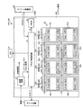
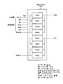
図1は、SSD100の構成例を示すブロック図である。SSD100は、システム基板(基板)120に搭載されたASICおよびNANDメモリ10で構成されている。また、ASICには、ドライブ制御回路4,電源回路5,DRAM20が搭載されている。
(1)8ビットノーマルモード
1Chだけ動作させ、8ビット単位で読み書きをするモードである。転送サイズの1単位はページサイズ(4kB)である。
(2)32ビットノーマルモード
4Ch並列で動作させ、32ビット単位で読み書きをするモードである。転送サイズの1単位はページサイズ×4(16kB)である。
(3)32ビット倍速モード
4Ch並列で動作させ、更に、NANDメモリ10の倍速モードを利用して読み書きをするモードである。転送サイズの1単位はページサイズ×4×2(32kB)である。
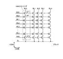
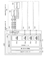
図4は、NAND I/F116とNANDメモリ10との接続を説明するための図である。NAND I/F116は、4Chのインタフェース回路であるCh0〜Ch3制御部210a〜210dを備えており、Ch0〜Ch3制御部210a〜210dの制御信号ピン201およびIO信号ピン202は、Ch0〜Ch3のNANDパッケージ10a〜10d(NAND Ch0〜Ch3)とそれぞれ独立に接続されている。制御信号ピン201からは制御信号が出力され、IOピン202からは8ビットのデータIO0〜7が入出力される。CE(チップイネーブル)0〜3信号は、NANDパッケージ10a〜10d(NAND Ch0〜Ch3)を選択する。
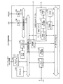
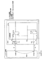
図11〜図15を参照して、NANDメモリ10のアクセス時に、信号線の負荷容量を低減して信号遅延を防止する方法について説明する。本実施の形態では、NANDコントローラ112とChip間の信号線の接続を切り替えるバススイッチを設け、NANDメモリ10のリード/ライト時にアクセスしないChipとの接続を遮断することにより、リード/ライト時の信号線の負荷容量を低減して信号遅延を防止する。
図11は、実施例1に係るNANDコントローラ112およびNANDメモリ10を説明するための図である。図11において、上記図6と同様の機能を有する部位には同一符号を付しており、共通する部分の説明を省略する。実施例1は、図11に示すように、システム基板上120にバススイッチ300aを設けた構成である。なお、同図では、Ch0のみを図示しているが、他のCh1〜3についても同様にバススイッチが設けられている。また、同図において、217は出力IOを示している。
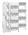
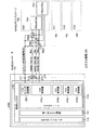
上記実施例1は、システム基板上120にバススイッチ300aを設けた構成である。これに対して、実施例2は、各NANDメモリパッケージ10a〜10dの内部にバススイッチを設けた構成である。図12は、実施例2に係るNANDメモリ10を説明するための図である。同図では、NANDメモリパッケージ10aのみを示しているが、NANDメモリパッケージ10b〜10dも同様な構成である。
上記実施例2では、バススイッチ301a1、301a2がアクセスアドレスに基づいてアクセスするChipを選択する構成である。これに対して、実施例3は、バススイッチがNANDコントローラ112から入力されるバススイッチ切替信号SELに基づいて、Chipの接続の切り替えを行う構成である。図14は、実施例3に係るNANDメモリ10を説明するための図である。同図では、NANDメモリパッケージ10aのみを示しているが、NANDメモリパッケージ10b〜10dも同様な構成である。
上記実施例2は、バススイッチによりNANDメモリ10の1つのChip単位で接続を切り替える構成である。これに対して、実施例4は、バススイッチによりNANDメモリ10の複数チップ単位で接続を切り替える構成である。図15は、実施例4に係るNANDメモリ10を説明するための図である。同図では、NANDメモリパッケージ10aのみを示しているが、NANDメモリパッケージ10b〜10dも同様な構成である。
1 ホスト装置
2 ATAインタフェース(ATA I/F)
3 RS232C I/F
4 ドライブ制御回路
5 電源回路
6 LED
10 NANDメモリ
10a〜d NANDメモリパッケージ
10a1,10a2〜10d1,10d2 8StackChip
20 DRAM
101 データアクセス用バス
102 第1の回路制御用バス
103 第2の回路制御用バス
104 プロセッサ
105 ブートROM
106 ROMコントローラ
107 クロックコントローラ
108 パラレルIO(PIO)回路
109 シリアルIO(SIO)回路
110 ATAインタフェースコントローラ(ATAコントローラ)
111 第2のECC(Error Check and Correct)回路
112 NANDコントローラ
113 DRAMコントローラ
114 SRAM
115 SRAMコントローラ
116 NAND I/F
117 第1のECC回路
118 DMAコントローラ
119 制御レジスタ
120 システム基板
220 バススイッチ制御部
300a,301a,302a,303a,304a バススイッチ
Claims (5)
- 複数の不揮発性メモリチップが搭載される不揮発性記憶部と、前記不揮発性記憶部を制御するコントロール回路と、前記コントロール回路を制御するMPUと、ホストとの通信を行うインタフェース回路とが基板上に搭載されるメモリシステムにおいて、
前記コントロール回路と前記複数の不揮発性メモリチップ間の信号線の接続を切り替えるバススイッチを備えたことを特徴とするメモリシステム。 - 前記バススイッチは、前記基板上または前記不揮発性記憶部に搭載されることを特徴とする請求項1に記載のメモリシステム。
- 前記コントロール回路は、リード/ライトアドレスに応じて、前記バススイッチの切り替えを指示するバススイッチ切替信号を前記バススイッチに出力するバススイッチ制御部を含み、
前記バススイッチは、前記バススイッチ切替信号に基づいて、前記信号線の接続の切り替えを行うことを特徴とする請求項1または請求項2に記載のメモリシステム。 - 前記バススイッチは、リード/ライトアドレスに応じて、前記信号線の接続の切り替えを行うことを特徴とする請求項1または請求項2に記載のメモリシステム。
- 前記バススイッチは、1または複数の不揮発性メモリチップ単位で前記信号線の接続の切り替えを行うことを特徴とする請求項1〜請求項4のいずれか1つに記載のメモリシステム。
Priority Applications (11)
| Application Number | Priority Date | Filing Date | Title |
|---|---|---|---|
| JP2008162281A JP5253901B2 (ja) | 2008-06-20 | 2008-06-20 | メモリシステム |
| US12/435,671 US8595410B2 (en) | 2008-06-20 | 2009-05-05 | Memory system and bus switch |
| US14/063,278 US8832362B2 (en) | 2008-06-20 | 2013-10-25 | Memory system controlling load capacity |
| US14/335,361 US9280461B2 (en) | 2008-06-20 | 2014-07-18 | Memory system with selective access to first and second memories |
| US15/012,549 US20160147455A1 (en) | 2008-06-20 | 2016-02-01 | Memory system with selective access to first and second memories |
| US15/865,881 US10474360B2 (en) | 2008-06-20 | 2018-01-09 | Memory system with selective access to first and second memories |
| US16/671,674 US10956039B2 (en) | 2008-06-20 | 2019-11-01 | Memory system with selective access to first and second memories |
| US17/207,021 US11494077B2 (en) | 2008-06-20 | 2021-03-19 | Memory system with selective access to first and second memories |
| US17/979,042 US11836347B2 (en) | 2008-06-20 | 2022-11-02 | Memory system with selective access to first and second memories |
| US18/527,894 US12242723B2 (en) | 2008-06-20 | 2023-12-04 | Memory system with selective access to first and second memories |
| US19/023,991 US20250165141A1 (en) | 2008-06-20 | 2025-01-16 | Memory system with selective access to first and second memories |
Applications Claiming Priority (1)
| Application Number | Priority Date | Filing Date | Title |
|---|---|---|---|
| JP2008162281A JP5253901B2 (ja) | 2008-06-20 | 2008-06-20 | メモリシステム |
Publications (2)
| Publication Number | Publication Date |
|---|---|
| JP2010003161A true JP2010003161A (ja) | 2010-01-07 |
| JP5253901B2 JP5253901B2 (ja) | 2013-07-31 |
Family
ID=41432437
Family Applications (1)
| Application Number | Title | Priority Date | Filing Date |
|---|---|---|---|
| JP2008162281A Expired - Fee Related JP5253901B2 (ja) | 2008-06-20 | 2008-06-20 | メモリシステム |
Country Status (2)
| Country | Link |
|---|---|
| US (10) | US8595410B2 (ja) |
| JP (1) | JP5253901B2 (ja) |
Cited By (7)
| Publication number | Priority date | Publication date | Assignee | Title |
|---|---|---|---|---|
| WO2013046463A1 (ja) | 2011-09-30 | 2013-04-04 | 株式会社日立製作所 | 不揮発半導体記憶システム |
| WO2014061055A1 (en) | 2012-10-15 | 2014-04-24 | Hitachi, Ltd. | Storage sysyem which includes non-volatile semiconductor storage medium, and storage control method of storage system |
| JP2014211875A (ja) * | 2013-04-19 | 2014-11-13 | 創惟科技股▲ふん▼有限公司 | データアクセスシステム、データアクセス装置及びデータアクセスコントローラ |
| JP2015038761A (ja) * | 2014-10-15 | 2015-02-26 | 株式会社日立製作所 | 不揮発半導体記憶システム |
| JP2016006655A (ja) * | 2015-07-17 | 2016-01-14 | 株式会社日立製作所 | 不揮発半導体記憶システム |
| WO2016072007A1 (ja) * | 2014-11-07 | 2016-05-12 | 株式会社日立製作所 | 半導体メモリデバイス、ストレージシステム及び計算機 |
| JPWO2018055768A1 (ja) * | 2016-09-26 | 2018-10-25 | 株式会社日立製作所 | 半導体記憶装置 |
Families Citing this family (23)
| Publication number | Priority date | Publication date | Assignee | Title |
|---|---|---|---|---|
| JP5323199B2 (ja) | 2009-02-12 | 2013-10-23 | 株式会社東芝 | メモリシステム及びメモリシステムの制御方法 |
| KR101046806B1 (ko) * | 2009-05-29 | 2011-07-06 | 주식회사 하이닉스반도체 | 반도체 메모리 장치 |
| US20110047318A1 (en) * | 2009-08-19 | 2011-02-24 | Dmitroca Robert W | Reducing capacitive load in a large memory array |
| JP5624578B2 (ja) | 2012-03-23 | 2014-11-12 | 株式会社東芝 | メモリシステム |
| JP2014026529A (ja) * | 2012-07-27 | 2014-02-06 | Fujitsu Ltd | ストレージシステムおよびその制御方法 |
| US9471484B2 (en) | 2012-09-19 | 2016-10-18 | Novachips Canada Inc. | Flash memory controller having dual mode pin-out |
| US20140223213A1 (en) * | 2013-02-05 | 2014-08-07 | Kabushiki Kaisha Toshiba | Memory system |
| JP6067541B2 (ja) * | 2013-11-08 | 2017-01-25 | 株式会社東芝 | メモリシステムおよびメモリシステムのアセンブリ方法 |
| JP2015219643A (ja) * | 2014-05-15 | 2015-12-07 | キヤノン株式会社 | 画像処理装置、情報処理方法及びプログラム |
| CN104636656B (zh) * | 2015-02-11 | 2017-09-22 | 深圳市美贝壳科技有限公司 | 存储设备加载控制方法 |
| US9841904B2 (en) * | 2015-03-02 | 2017-12-12 | Samsung Electronics Co., Ltd. | Scalable and configurable non-volatile memory module array |
| KR20210035517A (ko) * | 2019-09-24 | 2021-04-01 | 에스케이하이닉스 주식회사 | 메모리 시스템 및 그것을 포함하는 데이터 처리 시스템 |
| US11734175B2 (en) | 2019-08-22 | 2023-08-22 | SK Hynix Inc. | Storage device and method of operating the same |
| KR102889618B1 (ko) | 2019-12-16 | 2025-11-24 | 에스케이하이닉스 주식회사 | 스토리지 장치 및 그 동작 방법 |
| US11762769B2 (en) | 2019-09-20 | 2023-09-19 | SK Hynix Inc. | Memory controller based on flush operation and method of operating the same |
| CN115004146B (zh) * | 2020-02-14 | 2025-09-19 | 华为技术有限公司 | 固态存储硬盘和固态存储硬盘的控制方法 |
| JP2022046887A (ja) * | 2020-09-11 | 2022-03-24 | キオクシア株式会社 | 半導体記憶装置 |
| US11508415B2 (en) * | 2021-03-15 | 2022-11-22 | Transcend Information, Inc. | Semiconductor memory package structure and semiconductor memory system |
| US12164782B2 (en) | 2021-03-29 | 2024-12-10 | SanDisk Technologies, Inc. | Persistent switch-based storage controller |
| US11675528B2 (en) | 2021-03-29 | 2023-06-13 | Western Digital Technologies, Inc. | Switch based BGA extension |
| CN113176964B (zh) * | 2021-04-29 | 2024-11-12 | 深圳忆联信息系统有限公司 | 基于mpu的ssd固件检错方法、装置、计算机设备及存储介质 |
| CN114003540A (zh) * | 2021-10-29 | 2022-02-01 | 深圳市信锐网科技术有限公司 | 一种数据采集装置、方法、设备及计算机可读存储介质 |
| CN115904254B (zh) * | 2023-01-09 | 2023-06-02 | 苏州浪潮智能科技有限公司 | 一种硬盘控制系统、方法及相关组件 |
Citations (4)
| Publication number | Priority date | Publication date | Assignee | Title |
|---|---|---|---|---|
| JP2002007201A (ja) * | 2000-06-21 | 2002-01-11 | Nec Corp | メモリシステム、メモリインターフェース及びメモリチップ |
| WO2002050690A2 (en) * | 2000-12-20 | 2002-06-27 | Thomson Licensing S.A. | I2c bus control for isolating selected ic's for fast i2 bus communication |
| JP2004199648A (ja) * | 2002-12-18 | 2004-07-15 | Hynix Semiconductor Inc | 複合型メモリ装置 |
| JP2006331310A (ja) * | 2005-05-30 | 2006-12-07 | Renesas Technology Corp | 半導体集積回路装置 |
Family Cites Families (25)
| Publication number | Priority date | Publication date | Assignee | Title |
|---|---|---|---|---|
| US5438536A (en) * | 1994-04-05 | 1995-08-01 | U.S. Robotics, Inc. | Flash memory module |
| US5603001A (en) * | 1994-05-09 | 1997-02-11 | Kabushiki Kaisha Toshiba | Semiconductor disk system having a plurality of flash memories |
| US5671388A (en) * | 1995-05-03 | 1997-09-23 | Intel Corporation | Method and apparatus for performing write operations in multi-level cell storage device |
| JP3688835B2 (ja) | 1996-12-26 | 2005-08-31 | 株式会社東芝 | データ記憶システム及び同システムに適用するデータ転送方法 |
| JP3822768B2 (ja) | 1999-12-03 | 2006-09-20 | 株式会社ルネサステクノロジ | Icカードの製造方法 |
| US6545929B1 (en) | 2000-08-31 | 2003-04-08 | Micron Technology, Inc. | Voltage regulator and data path for a memory device |
| JP2002251884A (ja) | 2001-02-21 | 2002-09-06 | Toshiba Corp | 半導体記憶装置及びそのシステム装置 |
| JP4256600B2 (ja) * | 2001-06-19 | 2009-04-22 | Tdk株式会社 | メモリコントローラ、メモリコントローラを備えるフラッシュメモリシステム及びフラッシュメモリの制御方法 |
| US6451626B1 (en) * | 2001-07-27 | 2002-09-17 | Charles W.C. Lin | Three-dimensional stacked semiconductor package |
| US6687147B2 (en) * | 2002-04-02 | 2004-02-03 | Hewlett-Packard Development Company, L.P. | Cubic memory array with diagonal select lines |
| US6542393B1 (en) * | 2002-04-24 | 2003-04-01 | Ma Laboratories, Inc. | Dual-bank memory module with stacked DRAM chips having a concave-shaped re-route PCB in-between |
| US20040049628A1 (en) * | 2002-09-10 | 2004-03-11 | Fong-Long Lin | Multi-tasking non-volatile memory subsystem |
| US20040245617A1 (en) * | 2003-05-06 | 2004-12-09 | Tessera, Inc. | Dense multichip module |
| US7590797B2 (en) * | 2004-04-08 | 2009-09-15 | Micron Technology, Inc. | System and method for optimizing interconnections of components in a multichip memory module |
| US7822912B2 (en) * | 2005-03-14 | 2010-10-26 | Phision Electronics Corp. | Flash storage chip and flash array storage system |
| US20070165457A1 (en) * | 2005-09-30 | 2007-07-19 | Jin-Ki Kim | Nonvolatile memory system |
| KR100755668B1 (ko) * | 2006-02-10 | 2007-09-05 | 삼성전자주식회사 | 반도체 칩 및 이를 포함하는 반도체 칩 패키지 |
| DE102006017947B4 (de) * | 2006-04-18 | 2008-02-21 | Qimonda Ag | Speicherbaustein, entsprechende Baugruppe sowie entsprechendes Herstellungsverfahren |
| JP4821426B2 (ja) * | 2006-05-11 | 2011-11-24 | 富士ゼロックス株式会社 | エラー回復プログラム、エラー回復装置及びコンピュータシステム |
| US7620784B2 (en) * | 2006-06-09 | 2009-11-17 | Microsoft Corporation | High speed nonvolatile memory device using parallel writing among a plurality of interfaces |
| US8102557B2 (en) * | 2006-11-13 | 2012-01-24 | Samsung Electronics Co., Ltd. | System and method for disabling access to non-volatile storage in a multi-function peripheral |
| KR100843546B1 (ko) * | 2006-11-21 | 2008-07-04 | 삼성전자주식회사 | 멀티 칩 패키지 플래시 메모리 장치 및 그것의 상태 신호독출 방법 |
| US8935302B2 (en) * | 2006-12-06 | 2015-01-13 | Intelligent Intellectual Property Holdings 2 Llc | Apparatus, system, and method for data block usage information synchronization for a non-volatile storage volume |
| KR100851545B1 (ko) * | 2006-12-29 | 2008-08-11 | 삼성전자주식회사 | 커맨드 및 어드레스 핀을 갖는 낸드 플래시 메모리 및그것을 포함한 플래시 메모리 시스템 |
| JP4999569B2 (ja) | 2007-06-18 | 2012-08-15 | ルネサスエレクトロニクス株式会社 | 半導体記憶装置 |
-
2008
- 2008-06-20 JP JP2008162281A patent/JP5253901B2/ja not_active Expired - Fee Related
-
2009
- 2009-05-05 US US12/435,671 patent/US8595410B2/en active Active
-
2013
- 2013-10-25 US US14/063,278 patent/US8832362B2/en active Active
-
2014
- 2014-07-18 US US14/335,361 patent/US9280461B2/en active Active
-
2016
- 2016-02-01 US US15/012,549 patent/US20160147455A1/en not_active Abandoned
-
2018
- 2018-01-09 US US15/865,881 patent/US10474360B2/en active Active
-
2019
- 2019-11-01 US US16/671,674 patent/US10956039B2/en active Active
-
2021
- 2021-03-19 US US17/207,021 patent/US11494077B2/en active Active
-
2022
- 2022-11-02 US US17/979,042 patent/US11836347B2/en active Active
-
2023
- 2023-12-04 US US18/527,894 patent/US12242723B2/en active Active
-
2025
- 2025-01-16 US US19/023,991 patent/US20250165141A1/en active Pending
Patent Citations (5)
| Publication number | Priority date | Publication date | Assignee | Title |
|---|---|---|---|---|
| JP2002007201A (ja) * | 2000-06-21 | 2002-01-11 | Nec Corp | メモリシステム、メモリインターフェース及びメモリチップ |
| WO2002050690A2 (en) * | 2000-12-20 | 2002-06-27 | Thomson Licensing S.A. | I2c bus control for isolating selected ic's for fast i2 bus communication |
| JP2004516576A (ja) * | 2000-12-20 | 2004-06-03 | トムソン ライセンシング ソシエテ アノニム | 高速i2cバス通信のために選択icを切り離すi2cバス制御 |
| JP2004199648A (ja) * | 2002-12-18 | 2004-07-15 | Hynix Semiconductor Inc | 複合型メモリ装置 |
| JP2006331310A (ja) * | 2005-05-30 | 2006-12-07 | Renesas Technology Corp | 半導体集積回路装置 |
Cited By (12)
| Publication number | Priority date | Publication date | Assignee | Title |
|---|---|---|---|---|
| WO2013046463A1 (ja) | 2011-09-30 | 2013-04-04 | 株式会社日立製作所 | 不揮発半導体記憶システム |
| US8949511B2 (en) | 2011-09-30 | 2015-02-03 | Hitachi, Ltd. | Nonvolatile semiconductor storage system |
| US9335929B2 (en) | 2011-09-30 | 2016-05-10 | Hitachi, Ltd. | Nonvolatile semiconductor storage system |
| WO2014061055A1 (en) | 2012-10-15 | 2014-04-24 | Hitachi, Ltd. | Storage sysyem which includes non-volatile semiconductor storage medium, and storage control method of storage system |
| US9092320B2 (en) | 2012-10-15 | 2015-07-28 | Hitachi, Ltd. | Storage system which includes non-volatile semiconductor storage medium, and storage control method of storage system |
| JP2014211875A (ja) * | 2013-04-19 | 2014-11-13 | 創惟科技股▲ふん▼有限公司 | データアクセスシステム、データアクセス装置及びデータアクセスコントローラ |
| JP2015038761A (ja) * | 2014-10-15 | 2015-02-26 | 株式会社日立製作所 | 不揮発半導体記憶システム |
| WO2016072007A1 (ja) * | 2014-11-07 | 2016-05-12 | 株式会社日立製作所 | 半導体メモリデバイス、ストレージシステム及び計算機 |
| US10157159B2 (en) | 2014-11-07 | 2018-12-18 | Hitachi, Ltd. | Semiconductor memory device, storage system, and computer |
| JP2016006655A (ja) * | 2015-07-17 | 2016-01-14 | 株式会社日立製作所 | 不揮発半導体記憶システム |
| JPWO2018055768A1 (ja) * | 2016-09-26 | 2018-10-25 | 株式会社日立製作所 | 半導体記憶装置 |
| US10614014B2 (en) | 2016-09-26 | 2020-04-07 | Hitachi, Ltd. | Semiconductor storage device having a memory controller, a selection unit and a switch unit connected to each other |
Also Published As
| Publication number | Publication date |
|---|---|
| US8832362B2 (en) | 2014-09-09 |
| US9280461B2 (en) | 2016-03-08 |
| US20230049754A1 (en) | 2023-02-16 |
| US20090319716A1 (en) | 2009-12-24 |
| US20160147455A1 (en) | 2016-05-26 |
| US20140052903A1 (en) | 2014-02-20 |
| US20200065000A1 (en) | 2020-02-27 |
| US20210208784A1 (en) | 2021-07-08 |
| US8595410B2 (en) | 2013-11-26 |
| US12242723B2 (en) | 2025-03-04 |
| US11836347B2 (en) | 2023-12-05 |
| US20240118804A1 (en) | 2024-04-11 |
| US20140331005A1 (en) | 2014-11-06 |
| US20250165141A1 (en) | 2025-05-22 |
| US10474360B2 (en) | 2019-11-12 |
| US11494077B2 (en) | 2022-11-08 |
| US10956039B2 (en) | 2021-03-23 |
| JP5253901B2 (ja) | 2013-07-31 |
| US20180129420A1 (en) | 2018-05-10 |
Similar Documents
| Publication | Publication Date | Title |
|---|---|---|
| JP5253901B2 (ja) | メモリシステム | |
| EP2248022B1 (en) | Memory system | |
| US8473760B2 (en) | Memory system and server system | |
| US10061527B2 (en) | Memory system and controller | |
| US10684672B2 (en) | Selection of a low power consumption mode in a memory system based on information on a data transfer state | |
| JP2012128816A (ja) | メモリシステム | |
| JP2008108418A (ja) | マルチページプログラムの方法、及びこれを行うためのフラッシュメモリ装置 | |
| US20180211707A1 (en) | Semiconductor memory device and method of controlling semiconductor memory device | |
| US8258817B2 (en) | Semiconductor integrated circuit | |
| US8558602B2 (en) | Semiconductor integrated circuit | |
| US20130173852A1 (en) | Memory system | |
| JP2012168719A (ja) | メモリシステム |
Legal Events
| Date | Code | Title | Description |
|---|---|---|---|
| A621 | Written request for application examination |
Free format text: JAPANESE INTERMEDIATE CODE: A621 Effective date: 20100914 |
|
| A131 | Notification of reasons for refusal |
Free format text: JAPANESE INTERMEDIATE CODE: A131 Effective date: 20120904 |
|
| A521 | Request for written amendment filed |
Free format text: JAPANESE INTERMEDIATE CODE: A523 Effective date: 20121105 |
|
| TRDD | Decision of grant or rejection written | ||
| A01 | Written decision to grant a patent or to grant a registration (utility model) |
Free format text: JAPANESE INTERMEDIATE CODE: A01 Effective date: 20130326 |
|
| A61 | First payment of annual fees (during grant procedure) |
Free format text: JAPANESE INTERMEDIATE CODE: A61 Effective date: 20130417 |
|
| R151 | Written notification of patent or utility model registration |
Ref document number: 5253901 Country of ref document: JP Free format text: JAPANESE INTERMEDIATE CODE: R151 |
|
| FPAY | Renewal fee payment (event date is renewal date of database) |
Free format text: PAYMENT UNTIL: 20160426 Year of fee payment: 3 |
|
| S111 | Request for change of ownership or part of ownership |
Free format text: JAPANESE INTERMEDIATE CODE: R313111 |
|
| R350 | Written notification of registration of transfer |
Free format text: JAPANESE INTERMEDIATE CODE: R350 |
|
| S111 | Request for change of ownership or part of ownership |
Free format text: JAPANESE INTERMEDIATE CODE: R313111 |
|
| R350 | Written notification of registration of transfer |
Free format text: JAPANESE INTERMEDIATE CODE: R350 |
|
| LAPS | Cancellation because of no payment of annual fees |