JP2010003161A - Memory system - Google Patents
Memory system Download PDFInfo
- Publication number
- JP2010003161A JP2010003161A JP2008162281A JP2008162281A JP2010003161A JP 2010003161 A JP2010003161 A JP 2010003161A JP 2008162281 A JP2008162281 A JP 2008162281A JP 2008162281 A JP2008162281 A JP 2008162281A JP 2010003161 A JP2010003161 A JP 2010003161A
- Authority
- JP
- Japan
- Prior art keywords
- nand
- bus switch
- memory
- signal
- nand memory
- Prior art date
- Legal status (The legal status is an assumption and is not a legal conclusion. Google has not performed a legal analysis and makes no representation as to the accuracy of the status listed.)
- Granted
Links
- 239000000758 substrate Substances 0.000 claims description 5
- 238000010586 diagram Methods 0.000 description 20
- 238000012937 correction Methods 0.000 description 13
- 238000012546 transfer Methods 0.000 description 7
- 238000001514 detection method Methods 0.000 description 5
- 230000006870 function Effects 0.000 description 5
- 238000012986 modification Methods 0.000 description 5
- 230000004048 modification Effects 0.000 description 5
- 239000004065 semiconductor Substances 0.000 description 5
- 238000013461 design Methods 0.000 description 3
- 239000007787 solid Substances 0.000 description 3
- 230000001360 synchronised effect Effects 0.000 description 3
- 230000003111 delayed effect Effects 0.000 description 2
- 230000004044 response Effects 0.000 description 2
- 238000004891 communication Methods 0.000 description 1
- 239000000470 constituent Substances 0.000 description 1
- 238000009792 diffusion process Methods 0.000 description 1
- 230000000694 effects Effects 0.000 description 1
- 230000005669 field effect Effects 0.000 description 1
- 229910044991 metal oxide Inorganic materials 0.000 description 1
- 150000004706 metal oxides Chemical class 0.000 description 1
- 238000000034 method Methods 0.000 description 1
- 238000012545 processing Methods 0.000 description 1
- 230000009467 reduction Effects 0.000 description 1
Images


Classifications
-
- G—PHYSICS
- G06—COMPUTING; CALCULATING OR COUNTING
- G06F—ELECTRIC DIGITAL DATA PROCESSING
- G06F3/00—Input arrangements for transferring data to be processed into a form capable of being handled by the computer; Output arrangements for transferring data from processing unit to output unit, e.g. interface arrangements
- G06F3/06—Digital input from, or digital output to, record carriers, e.g. RAID, emulated record carriers or networked record carriers
- G06F3/0601—Interfaces specially adapted for storage systems
- G06F3/0602—Interfaces specially adapted for storage systems specifically adapted to achieve a particular effect
- G06F3/0604—Improving or facilitating administration, e.g. storage management
-
- G—PHYSICS
- G06—COMPUTING; CALCULATING OR COUNTING
- G06F—ELECTRIC DIGITAL DATA PROCESSING
- G06F12/00—Accessing, addressing or allocating within memory systems or architectures
- G06F12/02—Addressing or allocation; Relocation
- G06F12/0223—User address space allocation, e.g. contiguous or non contiguous base addressing
- G06F12/023—Free address space management
- G06F12/0238—Memory management in non-volatile memory, e.g. resistive RAM or ferroelectric memory
- G06F12/0246—Memory management in non-volatile memory, e.g. resistive RAM or ferroelectric memory in block erasable memory, e.g. flash memory
-
- G—PHYSICS
- G06—COMPUTING; CALCULATING OR COUNTING
- G06F—ELECTRIC DIGITAL DATA PROCESSING
- G06F13/00—Interconnection of, or transfer of information or other signals between, memories, input/output devices or central processing units
- G06F13/14—Handling requests for interconnection or transfer
- G06F13/16—Handling requests for interconnection or transfer for access to memory bus
- G06F13/1668—Details of memory controller
- G06F13/1684—Details of memory controller using multiple buses
-
- G—PHYSICS
- G06—COMPUTING; CALCULATING OR COUNTING
- G06F—ELECTRIC DIGITAL DATA PROCESSING
- G06F13/00—Interconnection of, or transfer of information or other signals between, memories, input/output devices or central processing units
- G06F13/38—Information transfer, e.g. on bus
- G06F13/40—Bus structure
- G06F13/4004—Coupling between buses
- G06F13/4022—Coupling between buses using switching circuits, e.g. switching matrix, connection or expansion network
-
- G—PHYSICS
- G06—COMPUTING; CALCULATING OR COUNTING
- G06F—ELECTRIC DIGITAL DATA PROCESSING
- G06F3/00—Input arrangements for transferring data to be processed into a form capable of being handled by the computer; Output arrangements for transferring data from processing unit to output unit, e.g. interface arrangements
- G06F3/06—Digital input from, or digital output to, record carriers, e.g. RAID, emulated record carriers or networked record carriers
- G06F3/0601—Interfaces specially adapted for storage systems
- G06F3/0628—Interfaces specially adapted for storage systems making use of a particular technique
- G06F3/0629—Configuration or reconfiguration of storage systems
-
- G—PHYSICS
- G06—COMPUTING; CALCULATING OR COUNTING
- G06F—ELECTRIC DIGITAL DATA PROCESSING
- G06F3/00—Input arrangements for transferring data to be processed into a form capable of being handled by the computer; Output arrangements for transferring data from processing unit to output unit, e.g. interface arrangements
- G06F3/06—Digital input from, or digital output to, record carriers, e.g. RAID, emulated record carriers or networked record carriers
- G06F3/0601—Interfaces specially adapted for storage systems
- G06F3/0668—Interfaces specially adapted for storage systems adopting a particular infrastructure
- G06F3/0671—In-line storage system
- G06F3/0683—Plurality of storage devices
- G06F3/0688—Non-volatile semiconductor memory arrays
-
- G—PHYSICS
- G06—COMPUTING; CALCULATING OR COUNTING
- G06F—ELECTRIC DIGITAL DATA PROCESSING
- G06F2212/00—Indexing scheme relating to accessing, addressing or allocation within memory systems or architectures
- G06F2212/72—Details relating to flash memory management
- G06F2212/7202—Allocation control and policies
Landscapes
- Engineering & Computer Science (AREA)
- Theoretical Computer Science (AREA)
- Physics & Mathematics (AREA)
- General Engineering & Computer Science (AREA)
- General Physics & Mathematics (AREA)
- Human Computer Interaction (AREA)
- Mathematical Physics (AREA)
- Computer Hardware Design (AREA)
- Read Only Memory (AREA)
- Techniques For Improving Reliability Of Storages (AREA)
- Memory System (AREA)
Abstract
Description
本発明は、不揮発性半導体記憶装置を用いて構成されるメモリシステムに関する。 The present invention relates to a memory system configured using a nonvolatile semiconductor memory device.
コンピュータシステムに用いられる外部記憶装置として、フラッシュメモリ(フラッシュEEPROM)を搭載したメモリシステムとしてSSD(Solid State Drive)が注目されている。フラッシュメモリは、磁気ディスク装置に比べ、高速、軽量などの利点を有している。 As an external storage device used in a computer system, an SSD (Solid State Drive) has attracted attention as a memory system equipped with a flash memory (flash EEPROM). The flash memory has advantages such as high speed and light weight compared with the magnetic disk device.
SSD内には、複数のフラッシュメモリチップ、ホスト装置からの要求に応じて各フラッシュメモリチップのリード/ライト制御を行うコントローラ、各フラッシュメモリチップとホスト装置との間でデータ転送を行うためのバッファメモリ、電源回路、ホスト装置に対する接続インタフェースなどを備えている(例えば、特許文献1)。 The SSD includes a plurality of flash memory chips, a controller that performs read / write control of each flash memory chip in response to a request from the host device, and a buffer that performs data transfer between each flash memory chip and the host device. A memory, a power supply circuit, a connection interface for a host device, and the like are provided (for example, Patent Document 1).
しかしながら、SSDを設計する場合、コントローラチップのPin数や実装面積が限られた中で、データ容量を増やすために、メモリChipを複数枚Stack(積層)したStack品を使用する必要がある。かかるStack品では、内部でIO信号線および制御信号線をメモリChip数分纏めた形となり、各信号線の負荷容量もStackしたメモリChip数につれて大きくなる。 However, when designing an SSD, it is necessary to use a Stack product in which a plurality of memory chips are stacked in order to increase the data capacity in a limited number of Pins and mounting area of a controller chip. In such a Stack product, the IO signal lines and the control signal lines are integrated in the number corresponding to the number of the memory chips, and the load capacity of each signal line increases as the number of stacked memory chips.
各信号線の負荷容量が大きくなると、IO信号および制御信号のCR遅延による遅れが生じ、同期設計したコントローラを使用した場合、低負荷(Stack数:少)ではメモリからの読み取りデータをラッチして出力できるが、高負荷(Stack数:多)ではCR遅延によってメモリから読み出したデータの遅延のため、ラッチして出力できないおそれがある。同様に、各信号線の負荷容量が大きくなると、信号遅延のためにメモリに対する書き込みエラーが発生するおそれがある。 When the load capacity of each signal line becomes large, a delay due to the CR delay of the IO signal and the control signal occurs. When a synchronously designed controller is used, the read data from the memory is latched at a low load (number of stacks: small). Although it can be output, at high load (number of stacks: many), there is a possibility that the data read from the memory is delayed due to the CR delay and cannot be latched and output. Similarly, when the load capacity of each signal line increases, there is a possibility that a write error to the memory may occur due to signal delay.
本発明は、上記課題に鑑みてなされたものであり、不揮発性記憶部の信号線の負荷容量が増大した場合においても、信号遅延を防止することが可能なメモリシステムを提供することを目的とする。 The present invention has been made in view of the above problems, and an object of the present invention is to provide a memory system capable of preventing signal delay even when the load capacity of a signal line of a nonvolatile storage unit is increased. To do.
上述した課題を解決し、目的を達成するために、本発明は、複数の不揮発性メモリチップが搭載される不揮発性記憶部と、前記不揮発性記憶部を制御するコントロール回路と、前記コントロール回路を制御するMPUと、ホストとの通信を行うインタフェース回路とが基板上に搭載されるメモリシステムにおいて、前記コントロール回路と前記複数の不揮発性メモリチップ間の信号線の接続を切り替えるバススイッチを備えたことを特徴とする。 In order to solve the above-described problems and achieve the object, the present invention includes a nonvolatile memory unit on which a plurality of nonvolatile memory chips are mounted, a control circuit that controls the nonvolatile memory unit, and the control circuit. In a memory system in which an MPU to be controlled and an interface circuit that communicates with a host are mounted on a substrate, a bus switch that switches connection of signal lines between the control circuit and the plurality of nonvolatile memory chips is provided. It is characterized by.
本発明によれば、コントローラ回路と不揮発性記憶部に搭載される複数の不揮発性メモリチップ間の信号線の接続を切り替えるバススイッチを設けているので、不揮発性記憶部にアクセスする場合に、バススイッチにより、アクセスする不揮発性メモリチップを接続する一方、アクセスしない不揮発性メモリチップとの接続を遮断することができ、不揮発性記憶部に対するアクセス時の信号線の負荷容量を低減でき、不揮発性記憶部の信号線の負荷容量が増大した場合においても、信号遅延を防止することが可能なメモリシステムを提供することが可能となるという効果を奏する。 According to the present invention, the bus switch for switching the connection of the signal lines between the plurality of nonvolatile memory chips mounted on the controller circuit and the nonvolatile storage unit is provided. The switch can connect the non-volatile memory chip to be accessed while disconnecting the non-accessible non-volatile memory chip, and can reduce the load capacity of the signal line when accessing the non-volatile memory unit. Even in the case where the load capacity of the signal lines increases, it is possible to provide a memory system capable of preventing signal delay.
以下に、この発明につき図面を参照しつつ詳細に説明する。なお、この実施例によりこの発明が限定されるものではない。また、下記実施例における構成要素には、当業者が容易に想定できるものまたは実質的に同一のものが含まれる。 Hereinafter, the present invention will be described in detail with reference to the drawings. Note that the present invention is not limited to the embodiments. In addition, constituent elements in the following embodiments include those that can be easily assumed by those skilled in the art or those that are substantially the same.
本実施例のメモリシステムは、不揮発性半導体記憶装置を含み、たとえば、パーソナルコンピュータなどのホスト装置の2次記憶装置(SSD:Solid State Drive)として使用され、ホスト装置から書込要求が出されたデータを記憶し、またホスト装置から読出要求のあったデータを読出してホスト装置に出力する機能を有する。 The memory system of the present embodiment includes a nonvolatile semiconductor memory device, and is used as a secondary storage device (SSD: Solid State Drive) of a host device such as a personal computer, for example, and a write request is issued from the host device. It has a function of storing data and reading data requested to be read from the host device and outputting it to the host device.
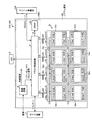
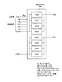
[SSDの構成例]
図1は、SSD100の構成例を示すブロック図である。SSD100は、システム基板(基板)120に搭載されたASICおよびNANDメモリ10で構成されている。また、ASICには、ドライブ制御回路4,電源回路5,DRAM20が搭載されている。
[Configuration example of SSD]
FIG. 1 is a block diagram illustrating a configuration example of the
SSD100は、ATAインタフェース(ATA I/F)2などのメモリ接続インタフェースを介してパソコンあるいはCPUコアなどのホスト装置(ホスト)1と接続され、ホスト装置1の外部メモリとして機能する。また、SSD100は、RS232Cインタフェース(RS232C I/F)3などの通信インタフェースを介して、デバッグ用機器200との間でデータを送受信することができる。SSD100は、不揮発性メモリとしてのNANDフラッシュメモリ(以下、NANDメモリと略す)10と、コントローラとしてのドライブ制御回路4と、揮発性メモリとしてのDRAM20と、電源回路5と、状態表示用のLED6などを備えている。
The SSD 100 is connected to a host device (host) 1 such as a personal computer or a CPU core via a memory connection interface such as an ATA interface (ATA I / F) 2 and functions as an external memory of the
電源回路5は、ホスト装置1側の電源回路から供給される外部直流電源から複数の異なる内部直流電源電圧を生成し、これら内部直流電源電圧をSSD100内の各回路に供給する。また、電源回路5は、外部電源の立ち上がりまたは立ち下がりを検知し、パワーオンリセット信号またはパワーオフリセット信号を生成して、ドライブ制御回路4に供給する。
The power supply circuit 5 generates a plurality of different internal DC power supply voltages from an external DC power supply supplied from the power supply circuit on the
NANDメモリ(不揮発性記憶部)10は、4ChのNANDメモリパッケージ10a〜10dを有する。1つのNANDメモリパッケージは、積層された複数のNANDメモリチップ(以下、「Chip」と称する)によって構成されている。図1に示す例では、例えば、NANDメモリパッケージ10aは、8枚のChip0〜7(例えば、1Chip=16GB)がStackされた8StackChip10a1と、8枚のChip8〜15がStackされた8StackChip10a2とを備え、他のNANDメモリパッケージ10b〜dも同様に、2組の8StackChipを備えており、NANDメモリ10は128GBの容量を有する。4ChのNANDメモリパッケージ10a〜10dは、4並列動作が可能となっている。
The NAND memory (nonvolatile storage unit) 10 includes 4Ch
DRAM20は、ホスト装置1とNANDメモリ10間でのデータ転送用キャッシュおよび作業領域用メモリとして機能する。ドライブ制御回路4は、ホスト装置1とNANDメモリ10との間でDRAM20を介してデータ転送制御を行うとともに、SSD100内の各構成要素を制御する。また、ドライブ制御回路4は、状態表示用LED6にステータス表示用信号を供給するとともに、電源回路5からのパワーオン/オフリセット信号を受けて、リセット信号およびクロック信号を自回路内およびSSD100内の各部に供給する機能も有している。
The DRAM 20 functions as a data transfer cache and work area memory between the
各NANDメモリチップは、データ消去の単位であるブロックを複数配列して構成されている。図2は、NANDメモリチップに含まれる1個のブロックの構成例を示す回路図である。各ブロックは、X方向に沿って順に配列された(m+1)個のNANDストリングを備えている(mは、0以上の整数)。(m+1)個のNANDストリングにそれぞれ含まれる選択トランジスタST1は、ドレインがビット線BL0〜BLmに接続され、ゲートが選択ゲート線SGDに共通接続されている。また、選択トランジスタST2は、ソースがソース線SLに共通接続され、ゲートが選択ゲート線SGSに共通接続されている。 Each NAND memory chip is configured by arranging a plurality of blocks which are data erasing units. FIG. 2 is a circuit diagram showing a configuration example of one block included in the NAND memory chip. Each block includes (m + 1) NAND strings arranged in order along the X direction (m is an integer of 0 or more). The select transistors ST1 included in each of (m + 1) NAND strings have drains connected to the bit lines BL0 to BLm and gates commonly connected to the select gate line SGD. In addition, the selection transistor ST2 has a source commonly connected to the source line SL and a gate commonly connected to the selection gate line SGS.
各メモリセルトランジスタMTは、半導体基板上に形成された積層ゲート構造を備えたMOSFET(metal oxide semiconductor field effect transistor)から構成される。積層ゲート構造は、半導体基板上にゲート絶縁膜を介在して形成された電荷蓄積層(浮遊ゲート電極)、及び電荷蓄積層上にゲート間絶縁膜を介在して形成された制御ゲート電極を含んでいる。メモリセルトランジスタMTは、浮遊ゲート電極に蓄えられる電子の数に応じて閾値電圧が変化し、この閾値電圧の違いに応じてデータを記憶する。メモリセルトランジスタMTは、1ビットを記憶するように構成されていてもよいし、多値(2ビット以上のデータ)を記憶するように構成されていてもよい。 Each memory cell transistor MT is composed of a MOSFET (metal oxide semiconductor field effect transistor) having a stacked gate structure formed on a semiconductor substrate. The stacked gate structure includes a charge storage layer (floating gate electrode) formed on a semiconductor substrate with a gate insulating film interposed therebetween, and a control gate electrode formed on the charge storage layer with an inter-gate insulating film interposed therebetween. It is out. In the memory cell transistor MT, the threshold voltage changes according to the number of electrons stored in the floating gate electrode, and data is stored according to the difference in threshold voltage. The memory cell transistor MT may be configured to store 1 bit, or may be configured to store multiple values (data of 2 bits or more).
各NANDストリングにおいて、(n+1)個のメモリセルトランジスタMTは、選択トランジスタST1のソースと選択トランジスタST2のドレインとの間に、それぞれの電流経路が直列接続されるように配置されている。すなわち、複数のメモリセルトランジスタMTは、隣接するもの同士で拡散領域(ソース領域若しくはドレイン領域)を共有するような形でY方向に直列接続される。 In each NAND string, (n + 1) memory cell transistors MT are arranged such that their current paths are connected in series between the source of the selection transistor ST1 and the drain of the selection transistor ST2. That is, the plurality of memory cell transistors MT are connected in series in the Y direction so that adjacent ones share a diffusion region (source region or drain region).
そして、最もドレイン側に位置するメモリセルトランジスタMTから順に、制御ゲート電極がワード線WL0〜WLnにそれぞれ接続されている。従って、ワード線WL0に接続されたメモリセルトランジスタMTのドレインは選択トランジスタST1のソースに接続され、ワード線WLnに接続されたメモリセルトランジスタMTのソースは選択トランジスタST2のドレインに接続されている。 The control gate electrodes are connected to the word lines WL0 to WLn in order from the memory cell transistor MT located closest to the drain side. Therefore, the drain of the memory cell transistor MT connected to the word line WL0 is connected to the source of the selection transistor ST1, and the source of the memory cell transistor MT connected to the word line WLn is connected to the drain of the selection transistor ST2.
ワード線WL0〜WLnは、ブロック内のNANDストリング間で、メモリセルトランジスタMTの制御ゲート電極を共通に接続している。つまり、ブロック内において同一行にあるメモリセルトランジスタMTの制御ゲート電極は、同一のワード線WLに接続される。この同一のワード線WLに接続される(m+1)個のメモリセルトランジスタMTは1ページとして取り扱われ、このページごとにデータの書き込み及びデータの読み出しが行われる。 The word lines WL0 to WLn connect the control gate electrodes of the memory cell transistors MT in common between the NAND strings in the block. That is, the control gate electrodes of the memory cell transistors MT in the same row in the block are connected to the same word line WL. The (m + 1) memory cell transistors MT connected to the same word line WL are handled as one page, and data writing and data reading are performed for each page.
また、ビット線BL0〜BLmは、ブロック間で、選択トランジスタST1のドレインを共通に接続している。つまり、複数のブロック内において同一列にあるNANDストリングは、同一のビット線BLに接続される。 The bit lines BL0 to BLm connect the drains of the selection transistors ST1 in common between the blocks. That is, NAND strings in the same column in a plurality of blocks are connected to the same bit line BL.
図1に示したように、NANDメモリ10においては、4つの並列動作要素であるNANDメモリパッケージ10a〜10dが各8ビットの4チャネル(4Ch)を介してドライブ制御回路4に並列接続されている。4つのNANDメモリパッケージ10a〜10dを単独動作させるか、並列動作させるか、NANDメモリ10の倍速モードを使用するか否か、という組み合わせにより、下記3種類のアクセスモードが提供される。
(1)8ビットノーマルモード
1Chだけ動作させ、8ビット単位で読み書きをするモードである。転送サイズの1単位はページサイズ(4kB)である。
(2)32ビットノーマルモード
4Ch並列で動作させ、32ビット単位で読み書きをするモードである。転送サイズの1単位はページサイズ×4(16kB)である。
(3)32ビット倍速モード
4Ch並列で動作させ、更に、NANDメモリ10の倍速モードを利用して読み書きをするモードである。転送サイズの1単位はページサイズ×4×2(32kB)である。
As shown in FIG. 1, in the
(1) 8-bit normal mode In this mode, only 1 Ch is operated and reading / writing is performed in 8-bit units. One unit of transfer size is a page size (4 kB).
(2) 32-bit normal mode This mode operates in 4Ch parallel and reads / writes in 32-bit units. One unit of the transfer size is page size × 4 (16 kB).
(3) 32-bit double speed mode This is a mode in which 4Ch is operated in parallel, and further, reading and writing are performed using the double speed mode of the
4Ch並列動作する32ビットノーマルモードまたは32ビット倍速モードでは、並列動作する4または8ブロックが、NANDメモリ10としての消去単位となり、並列動作する4または8ページが、NANDメモリ10としての書き込み単位及び読み出し単位となる。
In the 32-bit normal mode or the 32-bit double speed mode that operates in parallel with 4Ch, 4 or 8 blocks that operate in parallel serve as erase units as the
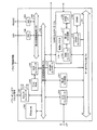
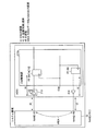
図3は、ドライブ制御回路4のハードウェア的な内部構成例を示すブロック図である。ドライブ制御回路4は、データアクセス用バス101、第1の回路制御用バス102、及び第2の回路制御用バス103を備えている。第1の回路制御用バス102には、ドライブ制御回路4全体を制御するプロセッサ104が接続されている。第1の回路制御用バス102には、NANDメモリ10に記憶された各管理プログラム(FW:ファームウエア)をブートするブート用プログラムが格納されたブートROM105がROMコントローラ106を介して接続されている。また、第1の回路制御用バス102には、図1に示した電源回路5からのパワーオン/オフリセット信号を受けて、リセット信号及びクロック信号を各部に供給するクロックコントローラ107が接続されている。
FIG. 3 is a block diagram illustrating an example of a hardware internal configuration of the drive control circuit 4. The drive control circuit 4 includes a data access bus 101, a first
第2の回路制御用バス103は、第1の回路制御用バス102に接続されている。第2の回路制御用バス103には、図1に示した状態表示用LED6にステータス表示用信号を供給するパラレルIO(PIO)回路108、RS232C I/F3を制御するシリアルIO(SIO)回路109が接続されている。
The second
ATAインタフェースコントローラ(ATAコントローラ)110、第2のECC(Error Check and Correct)回路111、NANDコントローラ112、及びDRAMコントローラ113は、データアクセス用バス101と第1の回路制御用バス102との両方に接続されている。ATAコントローラ110は、ATAインタフェース2を介してホスト装置1との間でデータを送受信する。データアクセス用バス101には、データ作業領域として使用されるSRAM114がSRAMコントローラ115を介して接続されている。SRAM114には、NANDメモリ10に記憶されているファームウエアが起動時、ブートROM105に記憶されたブート用プログラムによって転送される。
An ATA interface controller (ATA controller) 110, a second ECC (Error Check and Correct) circuit 111, a NAND controller 112, and a DRAM controller 113 are provided on both the data access bus 101 and the first
NANDコントローラ112は、NANDメモリ10の各NANDメモリパッケージ10a〜10dとのインタフェース処理を行うNAND I/F116、第1のECC回路117、NANDメモリ10−DRAM20間のアクセス制御を行うDMA転送制御用DMAコントローラ118、およびプロセッサ104により制御データが書き込まれる制御レジスタ119を備えている。
The NAND controller 112 is a DMA transfer control DMA that performs access control between the NAND I /
NANDメモリ10にデータを書き込む場合は、第1のECC回路117は、書き込み対象のデータに対して、所定単位データD(例えば、512B)毎に、誤り検出符号(例えば、CRC32)および1bitの訂正能力がある第1の誤り訂正符号(例えば、ハミング符号)を生成して付加する。また、第1のECC回路117は、8個の単位データD毎に、複数bit(例えば、48bit)の訂正能力がある第2の誤り訂正符号(例えば、BCH符号)を生成して付加する。誤り検出符号および第1の誤り訂正符号が付加されたデータがNAND I/F116によりNANDメモリ10に書き込まれる。
When writing data to the
また、NANDメモリ10からデータを読み出す場合は、第1のECC回路117は、NAND I/F116によりNANDメモリ10から読み出されたデータに対して、まず、第1の誤り訂正を行った後、誤り検出符号で誤りがあるか否かを検出し、第1の誤り訂正後のデータ、第1の誤り訂正による訂正bit数、および誤り検出結果を、DMAコントローラ118を介して、DRAM20に格納する。第2のECC回路111は、誤り検出結果で誤りがある場合に、すなわち、第1の誤り訂正で誤りを訂正できなかった場合に、第2の誤り訂正を行って、第2の誤り訂正後のデータおよび第2の誤り訂正による訂正bit数をDRAM20に格納する。
When reading data from the
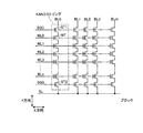
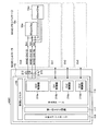
[NANDコントローラおよびNANDメモリ]
図4は、NAND I/F116とNANDメモリ10との接続を説明するための図である。NAND I/F116は、4Chのインタフェース回路であるCh0〜Ch3制御部210a〜210dを備えており、Ch0〜Ch3制御部210a〜210dの制御信号ピン201およびIO信号ピン202は、Ch0〜Ch3のNANDパッケージ10a〜10d(NAND Ch0〜Ch3)とそれぞれ独立に接続されている。制御信号ピン201からは制御信号が出力され、IOピン202からは8ビットのデータIO0〜7が入出力される。CE(チップイネーブル)0〜3信号は、NANDパッケージ10a〜10d(NAND Ch0〜Ch3)を選択する。
[NAND controller and NAND memory]
FIG. 4 is a diagram for explaining the connection between the NAND I /
以下の説明では、各Chの構成は同一であるので、Ch0を代表させて説明する。図5および図6は、NANDメモリ10の負荷容量およびCR遅延を説明するための図である。図6において、213は入出力IO,214および215は出力IOを示している。
In the following description, since the configuration of each Ch is the same, Ch0 will be described as a representative. 5 and 6 are diagrams for explaining the load capacity and CR delay of the
図5に示すように、8StackChip10a1は、IO信号(IOデータIO0〜7(アドレスデータを含む))、制御信号{WE(ライトイネーブル)信号、RE(リードイネーブル)信号、CLE(コマンドラッチイネーブル)信号、ALE(アドレスラッチイネーブル)信号、WP(ライトプロテクト)信号等}が1本/8Chipであるので、負荷容量が8倍に増加する。また、NANDパッケージ10aは、信号pinを減らすために、IO信号IO0〜7および制御信号/2個の8StackChip10a1,10a2としているため、負荷容量がさらに2倍に増加する。このため、CR遅延が増加する。また、一般に負荷容量はIO信号>制御信号であるため、IO信号と制御信号で遅延差が生じる。
As shown in FIG. 5, 8StackChip 10a1 includes IO signals (IO data IO0 to IO7 (including address data)), control signals {WE (write enable) signal, RE (read enable) signal, CLE (command latch enable) signal. , ALE (address latch enable) signal, WP (write protect) signal, etc.} is 1/8 chip, so that the
図7は、NANDメモリ10からのデータの読み出しを説明するためのタイミングチャートである。同図において、(A)はRE信号、(B)はIOデータを示している。ここで、システムは、RE信号の立ち下がりからtREA経過した後に、読み出しデータの出力が保証され、REの立ち上がりからtRLOH経過した後は、読み出しデータの出力が保証されないスペックであるとする。この場合、負荷容量が大きくCR遅延が大きい場合は、tREAが遅れ負荷容量が小さい場合のラッチタイミングではデータを取得できなくなってしまい、そのタイミング調整が必要となる。
FIG. 7 is a timing chart for explaining reading of data from the
図8〜図10を参照して、NAND I/F116のCh制御部に完全同期設計回路を搭載した場合の信号遅延について説明する。図8は、完全同期設計回路を説明するための図、図9は、負荷容量が小さい場合のタイミングチャート、図10は、負荷容量が大きい場合のタイミングチャートを示している。なお、以下、フリップフロップをFFと表記する。
With reference to FIGS. 8 to 10, signal delay in the case where a fully synchronous design circuit is mounted on the Ch control unit of the NAND I /
図8において、Ch0制御部210aは、クロックコントローラ107(図3参照)で生成された内部クロックCLKに同期してREを出力するFF_REと、内部クロックCLKに同期してIO[7:0]をラッチして出力するFF_DATA[7:0]とを備えている。同図において、t1は、IOとCR遅延、t2,t5は、伝搬(配線)遅延、t4はIO遅延、tREAはNANDデータ出力とIOとCR遅延を示している。
In FIG. 8, the
図9および図10において、(A)は内部CLK、(B)はFF_RE出力、(C)はNAND RE、(D)はNAND IO[7:0]、(E)はFF_DATA[7:0]入力、(F)はFF_DATA[7:0]出力を示している。 9A and 10B, (A) is the internal CLK, (B) is the FF_RE output, (C) is the NAND RE, (D) is NAND IO [7: 0], and (E) is FF_DATA [7: 0]. Input, (F) shows FF_DATA [7: 0] output.
図9に示すように、負荷容量が小さい場合には、t1およびtREAのCR遅延が小さいため、内部クロックCLKのタイミングでデータを取得することができる。他方、図10に示すように、負荷容量が大きい場合には、t1およびtREAのCR遅延が大きくなるため、内部クロックCLKのタイミングでデータを取得することができなくなってしまう。なお、ここでは、データリードの場合を説明したが、信号遅延によりライトエラーが発生する場合もある。このため、信号遅延を防止するために、NANDメモリ10のアクセス(リード/ライト)時に信号線(バスライン)の負荷容量を低減する必要がある。
As shown in FIG. 9, when the load capacity is small, the CR delay of t1 and tREA is small, so that data can be acquired at the timing of the internal clock CLK. On the other hand, as shown in FIG. 10, when the load capacity is large, the CR delay of t1 and tREA becomes large, and therefore data cannot be acquired at the timing of the internal clock CLK. Although the case of data read has been described here, a write error may occur due to signal delay. Therefore, in order to prevent signal delay, it is necessary to reduce the load capacity of the signal line (bus line) when the
[NANDメモリ10のリード/ライト時の負荷容量の低減]
図11〜図15を参照して、NANDメモリ10のアクセス時に、信号線の負荷容量を低減して信号遅延を防止する方法について説明する。本実施の形態では、NANDコントローラ112とChip間の信号線の接続を切り替えるバススイッチを設け、NANDメモリ10のリード/ライト時にアクセスしないChipとの接続を遮断することにより、リード/ライト時の信号線の負荷容量を低減して信号遅延を防止する。
[Reduction of load capacity during reading / writing of NAND memory 10]
With reference to FIGS. 11 to 15, a method of preventing signal delay by reducing the load capacity of the signal line when accessing the
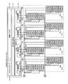
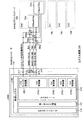
(実施例1)
図11は、実施例1に係るNANDコントローラ112およびNANDメモリ10を説明するための図である。図11において、上記図6と同様の機能を有する部位には同一符号を付しており、共通する部分の説明を省略する。実施例1は、図11に示すように、システム基板上120にバススイッチ300aを設けた構成である。なお、同図では、Ch0のみを図示しているが、他のCh1〜3についても同様にバススイッチが設けられている。また、同図において、217は出力IOを示している。
Example 1
FIG. 11 is a diagram for explaining the NAND controller 112 and the
実施例1では、システム基板板120上に、IO信号IO0〜7および制御信号(WE,RE、・・・)の信号線の接続を、8StackChip10a1と8StackChip10a2とで切り替えるためのバススイッチ300aを配置した。IO用のバススイッチ300aは、8ビット幅のスイッチが用いられており、制御信号用のバススイッチ300aは、1ビット幅のスイッチが用いられている。同図では、バススイッチ300aを模式的に示しており、バススイッチ300aは公知のバススイッチを使用することができるので、その詳細な説明を省略する。NANDコントローラ112のNAND I/F116は、バススイッチ300aの切り替えを制御するバススイッチ制御部220を備えている。
In the first embodiment, the
バススイッチ制御部220は、バススイッチ切替信号によりバススイッチ300aの切替制御を実行し、リード/ライト時のアドレスに応じてバススイッチ300aの上位(8StackChip10a1側)/下位(8StackChip10a2側)の切り替えを行う。バススイッチ制御部220は、プロセッサ104から8StackChip10a0側のアクセス命令がきた場合には、バススイッチ切替信号SEL=Lowを、8StackChip10a1側のアクセス命令がきた場合には、バススイッチ切替信号SEL=Highを、各バススイッチ300aに出力する。バススイッチ制御部220は、ch1〜ch3に設けられたバススイッチ(不図示)についても同様にその切り替えを制御する。
The bus
バススイッチ300aは、バススイッチ切替信号SEL=Lowの場合は、8StackChip10a1側を接続し、バススイッチ切替信号(SEL)=Highの場合は、8StackChip10a2側を接続する。
The
これにより、8StackChip10a1に対するリード/ライトの場合は、8StackChip10a2が切断された状態であり、また、8StackChip10a2に対するリード/ライトの場合は、8StackChip10a1が切断された状態であるので、リード/ライト時の信号線の負荷容量を1/2にすることができる。 As a result, when 8StackChip10a1 is read / written, 8StackChip10a2 is in a disconnected state, and when 8StackChip10a2 is read / written, 8StackChip10a1 is in a disconnected state. The load capacity can be halved.
なお、実施例1では、負荷の分割数を2つとしているが、本発明はこれに限られるものではなく、NANDコントローラ112のpin数やNANDメモリ10の負荷に応じて適宜分割することができる。
In the first embodiment, the number of load divisions is two. However, the present invention is not limited to this, and can be appropriately divided according to the number of pins of the NAND controller 112 and the load of the
(実施例2)
上記実施例1は、システム基板上120にバススイッチ300aを設けた構成である。これに対して、実施例2は、各NANDメモリパッケージ10a〜10dの内部にバススイッチを設けた構成である。図12は、実施例2に係るNANDメモリ10を説明するための図である。同図では、NANDメモリパッケージ10aのみを示しているが、NANDメモリパッケージ10b〜10dも同様な構成である。
(Example 2)
In the first embodiment, the
同図に示すように、NANDメモリパッケージ10aの内部には、8StackChip10a1のChip0〜7のいずれか1つを選択して接続するバススイッチ301a1と、8StackChip10a2のChip0〜7のいずれか1つを選択して接続するバススイッチ301a2とが設けられている。バススイッチ301a1、301a2は、アクセスアドレスに基づいてアクセスするChipを選択(デコード)し、選択したChipを接続する。実施例2では、バススイッチ301a1、301a2はアクセスアドレスに基づいてアクセスするChipを選択する構成であるので、実施例1のように、バススイッチ制御部220(図11参照)を設ける必要がなくなる。
As shown in the figure, inside the
実施例2では、IO信号用のバススイッチ301a、301bのみを示しているが、その他、WE/RE等の制御信号全てに対して、バススイッチを設けることにしてもよい。また、実施例2では、8StackChip10a1,10a2毎にバススイッチを設ける構成としたが、図13−1に示すように、8StackChip10a1,10a2のChipの接続の切り替えを1つのバススイッチ302aで行う構成としてもよい。また、図13−2に示すように、NANDメモリパッケージを1つの8StackChipで構成し、8StackChipに1つのバススイッチを設ける構成としてもよい。また、図13−3に示すように、8StackChip毎にNANDメモリパッケージを構成し、各8StackChipに1つのバススイッチを設けると共に、各8StackChipでChipが同時に選択されるのを防止するために、バススイッチ301a1、301a2に、CE(チップイネーブル)0〜3信号を入力する構成としてもよい。バススイッチ301a1、301a2はCE(チップイネーブル)0〜3信号に基づいてChip群を選択し、さらに、アクセスアドレスに基づいてアクセスするChipを選択(デコード)し、選択したChipを接続する。これにより、本実施例2によれば、実施例1の効果に加えて、コントローラ側がバススイッチを制御する必要がなり、またバススイッチがメモリに内蔵されるため部品数を減るため小型化を図ることができる。 In the second embodiment, only the IO signal bus switches 301a and 301b are shown, but other bus switches may be provided for all control signals such as WE / RE. In the second embodiment, a bus switch is provided for each of 8 StackChips 10a1 and 10a2. However, as shown in FIG. 13A, as shown in FIG. Good. Further, as illustrated in FIG. 13B, the NAND memory package may be configured by one 8StackChip, and one bus switch may be provided in the 8StackChip. Also, as shown in FIG. 13-3, a NAND memory package is configured for each 8 StackChip, one bus switch is provided for each 8StackChip, and in order to prevent the Chip from being simultaneously selected for each 8StackChip, CE (chip enable) 0 to 3 signals may be input to 301a1 and 301a2. The bus switches 301a1 and 301a2 select a Chip group based on CE (chip enable) 0 to 3 signals, select (decode) a Chip to be accessed based on an access address, and connect the selected Chip. As a result, according to the second embodiment, in addition to the effects of the first embodiment, the controller side needs to control the bus switch, and since the bus switch is built in the memory, the number of components is reduced and the size is reduced. be able to.
(実施例3)
上記実施例2では、バススイッチ301a1、301a2がアクセスアドレスに基づいてアクセスするChipを選択する構成である。これに対して、実施例3は、バススイッチがNANDコントローラ112から入力されるバススイッチ切替信号SELに基づいて、Chipの接続の切り替えを行う構成である。図14は、実施例3に係るNANDメモリ10を説明するための図である。同図では、NANDメモリパッケージ10aのみを示しているが、NANDメモリパッケージ10b〜10dも同様な構成である。
(Example 3)
In the second embodiment, the bus switches 301a1 and 301a2 select a chip to be accessed based on the access address. On the other hand, the third embodiment has a configuration in which the connection of the chip is switched based on the bus switch switching signal SEL input from the NAND controller 112 by the bus switch. FIG. 14 is a diagram for explaining the
同図において、バススイッチ303a1、303a2は、NANDコントローラ112から入力されるバススイッチ切替信号SELに基づいて、8StackChip10a1のChip0〜7および8StackChip10a2のChip0〜7のいずれか1つを接続する。これにより、信号線の負荷容量を低減して信号遅延を防止することができる。なお、実施例3においても、実施例2の変形例(図13−1〜図13−3)のように構成することにしてもよい。 In the figure, the bus switches 303a1 and 303a2 connect any one of Chip0 to Chip7 to 8StackChip10a1 and Chip0 to 7 to 8StackChip10a2 based on the bus switch switching signal SEL input from the NAND controller 112. Thereby, the load capacity of the signal line can be reduced and signal delay can be prevented. Note that the third embodiment may be configured as a modification of the second embodiment (FIGS. 13-1 to 13-3).
(実施例4)
上記実施例2は、バススイッチによりNANDメモリ10の1つのChip単位で接続を切り替える構成である。これに対して、実施例4は、バススイッチによりNANDメモリ10の複数チップ単位で接続を切り替える構成である。図15は、実施例4に係るNANDメモリ10を説明するための図である。同図では、NANDメモリパッケージ10aのみを示しているが、NANDメモリパッケージ10b〜10dも同様な構成である。
Example 4
In the second embodiment, the connection is switched in units of one chip of the
同図に示すように、8StackChip10a1は、Chip0〜3(チップ群)とChip4〜7(チップ群)の信号線がそれぞれ纏められており、すなわち、CE信号の単位毎(4Chip毎)に纏められている。同様に、8StackChip10a2の信号線もCE信号の単位毎(4Chip毎)に纏められている。バススイッチ304a1、304a2は、アクセスアドレスに基づいて、アクセスするChip群を選択し、選択したChip群に接続を切り替える。これにより、信号線の負荷容量を低減して信号遅延を防止することができる。なお、実施例4においても、実施例2の変形例(図13−1〜図13−3)のように構成することにしてもよい。
As shown in the figure, 8StackChip 10a1 has signal lines for
なお、実施例1〜実施例4は適宜組み合わせて実施可能であり、例えば、実施例1のように、システム基板120上にバススイッチを配置する場合においても、実施例2のように、バススイッチがアクセスアドレスに応じて信号線の接続を切り替える構成としてもよく、また、実施例2、4のように、バススイッチは、1または複数のChip単位で接続を切り替える構成としてもよい。
The first to fourth embodiments can be implemented in appropriate combinations. For example, when the bus switch is arranged on the
以上説明したように、本実施の形態によれば、NANDコントローラ112とNANDメモリ10に搭載される複数のChip間の信号線の接続を切り替えるバススイッチを設けているので、NANDメモリ10にアクセスする場合に、バススイッチにより、アクセスするChipを接続する一方、アクセスしないChipとの接続を遮断することができ、NANDメモリ10に対するアクセス時の信号線の負荷容量を低減でき、NANDメモリ10の信号線の負荷容量が増大した場合においても、信号遅延を防止することが可能となる。
As described above, according to the present embodiment, the bus switch for switching the connection of signal lines between a plurality of chips mounted on the NAND controller 112 and the
また、バススイッチをシステム基板120上またはNANDメモリ10に搭載することとしたので、SSD100のレイアウトを考慮して、バススイッチを配置する位置を決定することが可能となる。
In addition, since the bus switch is mounted on the
また、NANDコントローラ112のNAND I/F116にリード/ライトアドレスに応じて、バススイッチの切り替えを指示するバススイッチ切替信号をバススイッチに出力するバススイッチ制御部110を設け、バススイッチは、バススイッチ切替信号に基づいて信号線の接続の切り替えを行うこととしたので、バススイッチの構成を簡素化することが可能となる。
In addition, a bus switch control unit 110 is provided that outputs a bus switch switching signal to the NAND I /
また、バススイッチは、リード/ライトアドレスに応じて、信号線の接続の切り替えを行うこととしたので、NANDコントローラ112の構成を簡素化することが可能となる。 In addition, since the bus switch switches the connection of the signal lines according to the read / write address, the configuration of the NAND controller 112 can be simplified.
また、バススイッチは、1または複数のChip単位で信号線の接続の切り替えを行うこととしたので、NANDコントローラ112のpin数やNANDメモリ10の信号線の負荷容量に応じて、接続を切り替えるChip単位数を適宜選択することが可能となる。
In addition, since the bus switch switches the connection of the signal line in units of one or a plurality of chips, the connection is switched according to the number of pins of the NAND controller 112 and the load capacity of the signal line of the
なお、上記実施の形態では、本発明を、NANDメモリを有するSSDに適用するようにしたが、NOR型などの他のフラッシュEEPROMを有するSSDに本発明を適用するようにしてもよい。 In the above embodiment, the present invention is applied to an SSD having a NAND memory. However, the present invention may be applied to an SSD having another flash EEPROM such as a NOR type.
100 SSD
1 ホスト装置
2 ATAインタフェース(ATA I/F)
3 RS232C I/F
4 ドライブ制御回路
5 電源回路
6 LED
10 NANDメモリ
10a〜d NANDメモリパッケージ
10a1,10a2〜10d1,10d2 8StackChip
20 DRAM
101 データアクセス用バス
102 第1の回路制御用バス
103 第2の回路制御用バス
104 プロセッサ
105 ブートROM
106 ROMコントローラ
107 クロックコントローラ
108 パラレルIO(PIO)回路
109 シリアルIO(SIO)回路
110 ATAインタフェースコントローラ(ATAコントローラ)
111 第2のECC(Error Check and Correct)回路
112 NANDコントローラ
113 DRAMコントローラ
114 SRAM
115 SRAMコントローラ
116 NAND I/F
117 第1のECC回路
118 DMAコントローラ
119 制御レジスタ
120 システム基板
220 バススイッチ制御部
300a,301a,302a,303a,304a バススイッチ
100 SSD
1
3 RS232C I / F
4 Drive control circuit 5 Power supply circuit 6 LED
10
20 DRAM
101
106
111 Second ECC (Error Check and Correct) circuit 112 NAND controller 113 DRAM controller 114 SRAM
115
117
Claims (5)
前記コントロール回路と前記複数の不揮発性メモリチップ間の信号線の接続を切り替えるバススイッチを備えたことを特徴とするメモリシステム。 A non-volatile memory unit on which a plurality of non-volatile memory chips are mounted, a control circuit that controls the non-volatile memory unit, an MPU that controls the control circuit, and an interface circuit that communicates with a host are provided on a substrate. In the installed memory system,
A memory system comprising a bus switch for switching connection of signal lines between the control circuit and the plurality of nonvolatile memory chips.
前記バススイッチは、前記バススイッチ切替信号に基づいて、前記信号線の接続の切り替えを行うことを特徴とする請求項1または請求項2に記載のメモリシステム。 The control circuit includes a bus switch control unit that outputs a bus switch switching signal for instructing switching of the bus switch to the bus switch according to a read / write address;
The memory system according to claim 1, wherein the bus switch switches connection of the signal lines based on the bus switch switching signal.
Priority Applications (10)
| Application Number | Priority Date | Filing Date | Title |
|---|---|---|---|
| JP2008162281A JP5253901B2 (en) | 2008-06-20 | 2008-06-20 | Memory system |
| US12/435,671 US8595410B2 (en) | 2008-06-20 | 2009-05-05 | Memory system and bus switch |
| US14/063,278 US8832362B2 (en) | 2008-06-20 | 2013-10-25 | Memory system controlling load capacity |
| US14/335,361 US9280461B2 (en) | 2008-06-20 | 2014-07-18 | Memory system with selective access to first and second memories |
| US15/012,549 US20160147455A1 (en) | 2008-06-20 | 2016-02-01 | Memory system with selective access to first and second memories |
| US15/865,881 US10474360B2 (en) | 2008-06-20 | 2018-01-09 | Memory system with selective access to first and second memories |
| US16/671,674 US10956039B2 (en) | 2008-06-20 | 2019-11-01 | Memory system with selective access to first and second memories |
| US17/207,021 US11494077B2 (en) | 2008-06-20 | 2021-03-19 | Memory system with selective access to first and second memories |
| US17/979,042 US11836347B2 (en) | 2008-06-20 | 2022-11-02 | Memory system with selective access to first and second memories |
| US18/527,894 US20240118804A1 (en) | 2008-06-20 | 2023-12-04 | Memory system with selective access to first and second memories |
Applications Claiming Priority (1)
| Application Number | Priority Date | Filing Date | Title |
|---|---|---|---|
| JP2008162281A JP5253901B2 (en) | 2008-06-20 | 2008-06-20 | Memory system |
Publications (2)
| Publication Number | Publication Date |
|---|---|
| JP2010003161A true JP2010003161A (en) | 2010-01-07 |
| JP5253901B2 JP5253901B2 (en) | 2013-07-31 |
Family
ID=41432437
Family Applications (1)
| Application Number | Title | Priority Date | Filing Date |
|---|---|---|---|
| JP2008162281A Expired - Fee Related JP5253901B2 (en) | 2008-06-20 | 2008-06-20 | Memory system |
Country Status (2)
| Country | Link |
|---|---|
| US (9) | US8595410B2 (en) |
| JP (1) | JP5253901B2 (en) |
Cited By (7)
| Publication number | Priority date | Publication date | Assignee | Title |
|---|---|---|---|---|
| WO2013046463A1 (en) | 2011-09-30 | 2013-04-04 | 株式会社日立製作所 | Non-volatile semiconductor storage system |
| WO2014061055A1 (en) | 2012-10-15 | 2014-04-24 | Hitachi, Ltd. | Storage sysyem which includes non-volatile semiconductor storage medium, and storage control method of storage system |
| JP2014211875A (en) * | 2013-04-19 | 2014-11-13 | 創惟科技股▲ふん▼有限公司 | Data access system, data access device, and data access controller |
| JP2015038761A (en) * | 2014-10-15 | 2015-02-26 | 株式会社日立製作所 | Nonvolatile semiconductor storage system |
| JP2016006655A (en) * | 2015-07-17 | 2016-01-14 | 株式会社日立製作所 | Nonvolatile semiconductor storage system |
| WO2016072007A1 (en) * | 2014-11-07 | 2016-05-12 | 株式会社日立製作所 | Semiconductor memory device, storage system, and calculator |
| JPWO2018055768A1 (en) * | 2016-09-26 | 2018-10-25 | 株式会社日立製作所 | Semiconductor memory device |
Families Citing this family (20)
| Publication number | Priority date | Publication date | Assignee | Title |
|---|---|---|---|---|
| TWI432961B (en) | 2009-02-12 | 2014-04-01 | Toshiba Kk | Memory system and method of controlling memory system |
| KR101046806B1 (en) * | 2009-05-29 | 2011-07-06 | 주식회사 하이닉스반도체 | Semiconductor memory device |
| US20110047318A1 (en) * | 2009-08-19 | 2011-02-24 | Dmitroca Robert W | Reducing capacitive load in a large memory array |
| JP5624578B2 (en) | 2012-03-23 | 2014-11-12 | 株式会社東芝 | Memory system |
| JP2014026529A (en) * | 2012-07-27 | 2014-02-06 | Fujitsu Ltd | Storage system and control method thereof |
| US9471484B2 (en) | 2012-09-19 | 2016-10-18 | Novachips Canada Inc. | Flash memory controller having dual mode pin-out |
| US20140223213A1 (en) * | 2013-02-05 | 2014-08-07 | Kabushiki Kaisha Toshiba | Memory system |
| JP6067541B2 (en) * | 2013-11-08 | 2017-01-25 | 株式会社東芝 | Memory system and memory system assembly method |
| JP2015219643A (en) * | 2014-05-15 | 2015-12-07 | キヤノン株式会社 | Image processor, information processing method and program |
| CN104636656B (en) * | 2015-02-11 | 2017-09-22 | 深圳市美贝壳科技有限公司 | Storage device loading control method |
| US9841904B2 (en) * | 2015-03-02 | 2017-12-12 | Samsung Electronics Co., Ltd. | Scalable and configurable non-volatile memory module array |
| US11734175B2 (en) | 2019-08-22 | 2023-08-22 | SK Hynix Inc. | Storage device and method of operating the same |
| KR20210076497A (en) | 2019-12-16 | 2021-06-24 | 에스케이하이닉스 주식회사 | Storage device and operating method thereof |
| KR20210035517A (en) * | 2019-09-24 | 2021-04-01 | 에스케이하이닉스 주식회사 | Memory system and data processing system including the same |
| US11762769B2 (en) | 2019-09-20 | 2023-09-19 | SK Hynix Inc. | Memory controller based on flush operation and method of operating the same |
| CN115004146A (en) * | 2020-02-14 | 2022-09-02 | 华为技术有限公司 | Solid state storage hard disk and control method thereof |
| JP2022046887A (en) * | 2020-09-11 | 2022-03-24 | キオクシア株式会社 | Semiconductor storage device |
| US11508415B2 (en) * | 2021-03-15 | 2022-11-22 | Transcend Information, Inc. | Semiconductor memory package structure and semiconductor memory system |
| US11675528B2 (en) | 2021-03-29 | 2023-06-13 | Western Digital Technologies, Inc. | Switch based BGA extension |
| CN114003540A (en) * | 2021-10-29 | 2022-02-01 | 深圳市信锐网科技术有限公司 | Data acquisition device, method, equipment and computer readable storage medium |
Citations (4)
| Publication number | Priority date | Publication date | Assignee | Title |
|---|---|---|---|---|
| JP2002007201A (en) * | 2000-06-21 | 2002-01-11 | Nec Corp | Memory system, memory interface, and memory chip |
| WO2002050690A2 (en) * | 2000-12-20 | 2002-06-27 | Thomson Licensing S.A. | I2c bus control for isolating selected ic's for fast i2 bus communication |
| JP2004199648A (en) * | 2002-12-18 | 2004-07-15 | Hynix Semiconductor Inc | Composite memory device |
| JP2006331310A (en) * | 2005-05-30 | 2006-12-07 | Renesas Technology Corp | Semiconductor integrated circuit device |
Family Cites Families (21)
| Publication number | Priority date | Publication date | Assignee | Title |
|---|---|---|---|---|
| US5438536A (en) * | 1994-04-05 | 1995-08-01 | U.S. Robotics, Inc. | Flash memory module |
| US5603001A (en) * | 1994-05-09 | 1997-02-11 | Kabushiki Kaisha Toshiba | Semiconductor disk system having a plurality of flash memories |
| US5671388A (en) * | 1995-05-03 | 1997-09-23 | Intel Corporation | Method and apparatus for performing write operations in multi-level cell storage device |
| JP3688835B2 (en) | 1996-12-26 | 2005-08-31 | 株式会社東芝 | Data storage system and data transfer method applied to the system |
| JP3822768B2 (en) | 1999-12-03 | 2006-09-20 | 株式会社ルネサステクノロジ | IC card manufacturing method |
| US6545929B1 (en) | 2000-08-31 | 2003-04-08 | Micron Technology, Inc. | Voltage regulator and data path for a memory device |
| JP2002251884A (en) | 2001-02-21 | 2002-09-06 | Toshiba Corp | Semiconductor memory and system device therefor |
| JP4256600B2 (en) * | 2001-06-19 | 2009-04-22 | Tdk株式会社 | MEMORY CONTROLLER, FLASH MEMORY SYSTEM PROVIDED WITH MEMORY CONTROLLER, AND FLASH MEMORY CONTROL METHOD |
| US6451626B1 (en) * | 2001-07-27 | 2002-09-17 | Charles W.C. Lin | Three-dimensional stacked semiconductor package |
| US6687147B2 (en) * | 2002-04-02 | 2004-02-03 | Hewlett-Packard Development Company, L.P. | Cubic memory array with diagonal select lines |
| US6542393B1 (en) * | 2002-04-24 | 2003-04-01 | Ma Laboratories, Inc. | Dual-bank memory module with stacked DRAM chips having a concave-shaped re-route PCB in-between |
| US20040049628A1 (en) * | 2002-09-10 | 2004-03-11 | Fong-Long Lin | Multi-tasking non-volatile memory subsystem |
| US20040245617A1 (en) * | 2003-05-06 | 2004-12-09 | Tessera, Inc. | Dense multichip module |
| US7822912B2 (en) * | 2005-03-14 | 2010-10-26 | Phision Electronics Corp. | Flash storage chip and flash array storage system |
| DE102006017947B4 (en) * | 2006-04-18 | 2008-02-21 | Qimonda Ag | Memory module, corresponding module and corresponding manufacturing method |
| JP4821426B2 (en) * | 2006-05-11 | 2011-11-24 | 富士ゼロックス株式会社 | Error recovery program, error recovery device, and computer system |
| US7620784B2 (en) * | 2006-06-09 | 2009-11-17 | Microsoft Corporation | High speed nonvolatile memory device using parallel writing among a plurality of interfaces |
| US8102557B2 (en) * | 2006-11-13 | 2012-01-24 | Samsung Electronics Co., Ltd. | System and method for disabling access to non-volatile storage in a multi-function peripheral |
| KR100843546B1 (en) * | 2006-11-21 | 2008-07-04 | 삼성전자주식회사 | Multi-chip packaged flash memory device and reading method of status data thereof |
| US8935302B2 (en) * | 2006-12-06 | 2015-01-13 | Intelligent Intellectual Property Holdings 2 Llc | Apparatus, system, and method for data block usage information synchronization for a non-volatile storage volume |
| JP4999569B2 (en) | 2007-06-18 | 2012-08-15 | ルネサスエレクトロニクス株式会社 | Semiconductor memory device |
-
2008
- 2008-06-20 JP JP2008162281A patent/JP5253901B2/en not_active Expired - Fee Related
-
2009
- 2009-05-05 US US12/435,671 patent/US8595410B2/en active Active
-
2013
- 2013-10-25 US US14/063,278 patent/US8832362B2/en active Active
-
2014
- 2014-07-18 US US14/335,361 patent/US9280461B2/en active Active
-
2016
- 2016-02-01 US US15/012,549 patent/US20160147455A1/en not_active Abandoned
-
2018
- 2018-01-09 US US15/865,881 patent/US10474360B2/en active Active
-
2019
- 2019-11-01 US US16/671,674 patent/US10956039B2/en active Active
-
2021
- 2021-03-19 US US17/207,021 patent/US11494077B2/en active Active
-
2022
- 2022-11-02 US US17/979,042 patent/US11836347B2/en active Active
-
2023
- 2023-12-04 US US18/527,894 patent/US20240118804A1/en active Pending
Patent Citations (5)
| Publication number | Priority date | Publication date | Assignee | Title |
|---|---|---|---|---|
| JP2002007201A (en) * | 2000-06-21 | 2002-01-11 | Nec Corp | Memory system, memory interface, and memory chip |
| WO2002050690A2 (en) * | 2000-12-20 | 2002-06-27 | Thomson Licensing S.A. | I2c bus control for isolating selected ic's for fast i2 bus communication |
| JP2004516576A (en) * | 2000-12-20 | 2004-06-03 | トムソン ライセンシング ソシエテ アノニム | I2C bus control to disconnect selected IC for high-speed I2C bus communication |
| JP2004199648A (en) * | 2002-12-18 | 2004-07-15 | Hynix Semiconductor Inc | Composite memory device |
| JP2006331310A (en) * | 2005-05-30 | 2006-12-07 | Renesas Technology Corp | Semiconductor integrated circuit device |
Cited By (12)
| Publication number | Priority date | Publication date | Assignee | Title |
|---|---|---|---|---|
| WO2013046463A1 (en) | 2011-09-30 | 2013-04-04 | 株式会社日立製作所 | Non-volatile semiconductor storage system |
| US8949511B2 (en) | 2011-09-30 | 2015-02-03 | Hitachi, Ltd. | Nonvolatile semiconductor storage system |
| US9335929B2 (en) | 2011-09-30 | 2016-05-10 | Hitachi, Ltd. | Nonvolatile semiconductor storage system |
| WO2014061055A1 (en) | 2012-10-15 | 2014-04-24 | Hitachi, Ltd. | Storage sysyem which includes non-volatile semiconductor storage medium, and storage control method of storage system |
| US9092320B2 (en) | 2012-10-15 | 2015-07-28 | Hitachi, Ltd. | Storage system which includes non-volatile semiconductor storage medium, and storage control method of storage system |
| JP2014211875A (en) * | 2013-04-19 | 2014-11-13 | 創惟科技股▲ふん▼有限公司 | Data access system, data access device, and data access controller |
| JP2015038761A (en) * | 2014-10-15 | 2015-02-26 | 株式会社日立製作所 | Nonvolatile semiconductor storage system |
| WO2016072007A1 (en) * | 2014-11-07 | 2016-05-12 | 株式会社日立製作所 | Semiconductor memory device, storage system, and calculator |
| US10157159B2 (en) | 2014-11-07 | 2018-12-18 | Hitachi, Ltd. | Semiconductor memory device, storage system, and computer |
| JP2016006655A (en) * | 2015-07-17 | 2016-01-14 | 株式会社日立製作所 | Nonvolatile semiconductor storage system |
| JPWO2018055768A1 (en) * | 2016-09-26 | 2018-10-25 | 株式会社日立製作所 | Semiconductor memory device |
| US10614014B2 (en) | 2016-09-26 | 2020-04-07 | Hitachi, Ltd. | Semiconductor storage device having a memory controller, a selection unit and a switch unit connected to each other |
Also Published As
| Publication number | Publication date |
|---|---|
| US9280461B2 (en) | 2016-03-08 |
| US10474360B2 (en) | 2019-11-12 |
| US11836347B2 (en) | 2023-12-05 |
| US20210208784A1 (en) | 2021-07-08 |
| US20140331005A1 (en) | 2014-11-06 |
| US20160147455A1 (en) | 2016-05-26 |
| US11494077B2 (en) | 2022-11-08 |
| US20230049754A1 (en) | 2023-02-16 |
| US20090319716A1 (en) | 2009-12-24 |
| US10956039B2 (en) | 2021-03-23 |
| US8595410B2 (en) | 2013-11-26 |
| US20200065000A1 (en) | 2020-02-27 |
| US20140052903A1 (en) | 2014-02-20 |
| JP5253901B2 (en) | 2013-07-31 |
| US20240118804A1 (en) | 2024-04-11 |
| US8832362B2 (en) | 2014-09-09 |
| US20180129420A1 (en) | 2018-05-10 |
Similar Documents
| Publication | Publication Date | Title |
|---|---|---|
| JP5253901B2 (en) | Memory system | |
| EP2248022B1 (en) | Memory system | |
| US8473760B2 (en) | Memory system and server system | |
| US10061527B2 (en) | Memory system and controller | |
| US10684672B2 (en) | Selection of a low power consumption mode in a memory system based on information on a data transfer state | |
| JP2012128816A (en) | Memory system | |
| JP2008108418A (en) | Flash memory device and method of programming multi-pages in the same | |
| US20180211707A1 (en) | Semiconductor memory device and method of controlling semiconductor memory device | |
| US8558602B2 (en) | Semiconductor integrated circuit | |
| US8258817B2 (en) | Semiconductor integrated circuit | |
| JP2013137674A (en) | Memory system | |
| US11538535B2 (en) | Apparatus for rapid data destruction | |
| JP2012168719A (en) | Memory system |
Legal Events
| Date | Code | Title | Description |
|---|---|---|---|
| A621 | Written request for application examination |
Free format text: JAPANESE INTERMEDIATE CODE: A621 Effective date: 20100914 |
|
| A131 | Notification of reasons for refusal |
Free format text: JAPANESE INTERMEDIATE CODE: A131 Effective date: 20120904 |
|
| A521 | Request for written amendment filed |
Free format text: JAPANESE INTERMEDIATE CODE: A523 Effective date: 20121105 |
|
| TRDD | Decision of grant or rejection written | ||
| A01 | Written decision to grant a patent or to grant a registration (utility model) |
Free format text: JAPANESE INTERMEDIATE CODE: A01 Effective date: 20130326 |
|
| A61 | First payment of annual fees (during grant procedure) |
Free format text: JAPANESE INTERMEDIATE CODE: A61 Effective date: 20130417 |
|
| R151 | Written notification of patent or utility model registration |
Ref document number: 5253901 Country of ref document: JP Free format text: JAPANESE INTERMEDIATE CODE: R151 |
|
| FPAY | Renewal fee payment (event date is renewal date of database) |
Free format text: PAYMENT UNTIL: 20160426 Year of fee payment: 3 |
|
| S111 | Request for change of ownership or part of ownership |
Free format text: JAPANESE INTERMEDIATE CODE: R313111 |
|
| R350 | Written notification of registration of transfer |
Free format text: JAPANESE INTERMEDIATE CODE: R350 |
|
| S111 | Request for change of ownership or part of ownership |
Free format text: JAPANESE INTERMEDIATE CODE: R313111 |
|
| R350 | Written notification of registration of transfer |
Free format text: JAPANESE INTERMEDIATE CODE: R350 |
|
| LAPS | Cancellation because of no payment of annual fees |