JP2010002302A - 検査用接触構造体 - Google Patents
検査用接触構造体 Download PDFInfo
- Publication number
- JP2010002302A JP2010002302A JP2008161559A JP2008161559A JP2010002302A JP 2010002302 A JP2010002302 A JP 2010002302A JP 2008161559 A JP2008161559 A JP 2008161559A JP 2008161559 A JP2008161559 A JP 2008161559A JP 2010002302 A JP2010002302 A JP 2010002302A
- Authority
- JP
- Japan
- Prior art keywords
- ground conductor
- contact
- wiring layer
- inspection
- elastic
- Prior art date
- Legal status (The legal status is an assumption and is not a legal conclusion. Google has not performed a legal analysis and makes no representation as to the accuracy of the status listed.)
- Granted
Links
Images


Classifications
-
- G—PHYSICS
- G01—MEASURING; TESTING
- G01R—MEASURING ELECTRIC VARIABLES; MEASURING MAGNETIC VARIABLES
- G01R1/00—Details of instruments or arrangements of the types included in groups G01R5/00 - G01R13/00 and G01R31/00
- G01R1/02—General constructional details
- G01R1/06—Measuring leads; Measuring probes
- G01R1/067—Measuring probes
- G01R1/073—Multiple probes
- G01R1/07307—Multiple probes with individual probe elements, e.g. needles, cantilever beams or bump contacts, fixed in relation to each other, e.g. bed of nails fixture or probe card
- G01R1/07364—Multiple probes with individual probe elements, e.g. needles, cantilever beams or bump contacts, fixed in relation to each other, e.g. bed of nails fixture or probe card with provisions for altering position, number or connection of probe tips; Adapting to differences in pitch
- G01R1/07371—Multiple probes with individual probe elements, e.g. needles, cantilever beams or bump contacts, fixed in relation to each other, e.g. bed of nails fixture or probe card with provisions for altering position, number or connection of probe tips; Adapting to differences in pitch using an intermediate card or back card with apertures through which the probes pass
-
- G—PHYSICS
- G01—MEASURING; TESTING
- G01R—MEASURING ELECTRIC VARIABLES; MEASURING MAGNETIC VARIABLES
- G01R1/00—Details of instruments or arrangements of the types included in groups G01R5/00 - G01R13/00 and G01R31/00
- G01R1/02—General constructional details
- G01R1/06—Measuring leads; Measuring probes
- G01R1/067—Measuring probes
- G01R1/06772—High frequency probes
Abstract
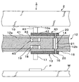
【解決手段】接地された接地導体部12の下面には、弾性接触部13が設けられている。弾性接触部13は、絶縁層15と、配線層16と、接触子17と、接触子17に対応した位置に設けられた弾性体18を有している。弾性体18は、弾性接触部13に電極Pに接触する際の弾性を付加している。弾性接触部13は、接地導体部12に平行に配置されている。配線層16と、接地導体部12とは、マイクロストリップ線路を形成する。
【選択図】図2
Description
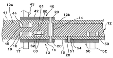
2 プローブカード
3 載置台
10 回路基板
10a 接続端子
11 検査用接触構造体
12 接地導体部
12a 本体
12b 貫通孔
13 弾性接触部
14 導電線
15 絶縁層
16 配線層
17 接触子
18 弾性体
19 窪み部
20 導体
21 絶縁層
40 弾性接触部
41 絶縁層
42 配線層
43 接触子
44 弾性体
45 窪み部
50 弾性接触体
51 配線層
52 接触子
53 弾性体
54 接続口
W ウェハ
P 検査用電極
Claims (8)
- 回路基板の下面に設けられ、被検査体の電気的特性を検査する検査用接触構造体であって、
接地された接地導体部と、前記被検査体と接触する弾性接触部と、前記回路基板と前記弾性接触部とを電気的に接続する導電線と、を有し、
前記弾性接触部は前記接地導体部の下面に設けられ、
前記弾性接触部は、
被検査体と接触する接触子と、
前記接触子と前記導電線とを電気的に接続する配線層と、
前記配線層と前記接地導体部の間に設けられた絶縁層と、
前記接触子を挟んで、被検査体と対向する位置に設けられた弾性体と、を備え、
前記配線層は、前記接地導体部と平行に配置されていることを特徴とする、検査用接触構造体。 - 前記接地導体部は、金属性の基板であることを特徴とする、請求項1に記載の検査用接触構造体。
- 前記接地導体部は、絶縁体と、前記絶縁体の表面に接合された導体と、を有することを特徴とする、請求項1に記載の検査用接触構造体。
- 前記接地導体部には、上下方向に貫通する貫通孔が形成され、
前記導電線は、前記貫通孔内において当該貫通孔と同軸状に設けられていることを特徴とする、請求項1〜3のいずれかに記載の検査用接触構造体。 - 前記接地導体部の上面には、他の弾性接触部がさらに設けられ、
前記他の弾性接触部は、
前記回路基板に接触する他の接触子と、
前記他の接触子と前記導電線とを電気的に接続する他の配線層と、
前記他の配線層と前記接地導体部の間に設けられた他の絶縁層と、
前記他の接触子を挟んで、前記回路基板と対向する位置に設けられた他の弾性体と、を備え、
前記回路基板と前記導電線とは、前記他の弾性接触部の接触子が、前記回路基板に接触することで、電気的に接続されていることを特徴とする、請求項1〜4のいずれかに記載の検査用接触構造体。 - 前記接地導体部の下面には、窪み部が形成され、
前記弾性体は、前記窪み部に配置されていることを特徴とする、請求項1〜5のいずれかに記載の検査用接触構造体。 - 前記接地導体部の下面には、他の窪み部が形成され、
当該他の窪み部には、前記配線層に接続されるノイズ除去用のコンデンサが配置されていることを特徴とする、請求項1〜6のいずれかに記載の検査用接触構造体。 - 前記弾性接触部の配線層は、前記接地導体部に電気的に接続されていることを特徴とする、請求項1〜7のいずれかに記載の検査用接触構造体。
Priority Applications (5)
| Application Number | Priority Date | Filing Date | Title |
|---|---|---|---|
| JP2008161559A JP5374079B2 (ja) | 2008-06-20 | 2008-06-20 | 検査用接触構造体 |
| KR1020107028137A KR101186915B1 (ko) | 2008-06-20 | 2009-06-17 | 검사용 접촉 구조체 |
| PCT/JP2009/061003 WO2009154217A1 (ja) | 2008-06-20 | 2009-06-17 | 検査用接触構造体 |
| US12/999,375 US8866506B2 (en) | 2008-06-20 | 2009-06-17 | Contact structure for inspection |
| TW98120527A TWI403724B (zh) | 2008-06-20 | 2009-06-19 | Inspection contact structure |
Applications Claiming Priority (1)
| Application Number | Priority Date | Filing Date | Title |
|---|---|---|---|
| JP2008161559A JP5374079B2 (ja) | 2008-06-20 | 2008-06-20 | 検査用接触構造体 |
Publications (2)
| Publication Number | Publication Date |
|---|---|
| JP2010002302A true JP2010002302A (ja) | 2010-01-07 |
| JP5374079B2 JP5374079B2 (ja) | 2013-12-25 |
Family
ID=41434134
Family Applications (1)
| Application Number | Title | Priority Date | Filing Date |
|---|---|---|---|
| JP2008161559A Expired - Fee Related JP5374079B2 (ja) | 2008-06-20 | 2008-06-20 | 検査用接触構造体 |
Country Status (5)
| Country | Link |
|---|---|
| US (1) | US8866506B2 (ja) |
| JP (1) | JP5374079B2 (ja) |
| KR (1) | KR101186915B1 (ja) |
| TW (1) | TWI403724B (ja) |
| WO (1) | WO2009154217A1 (ja) |
Cited By (3)
| Publication number | Priority date | Publication date | Assignee | Title |
|---|---|---|---|---|
| JP2011226963A (ja) * | 2010-04-21 | 2011-11-10 | Shinko Electric Ind Co Ltd | プローブカード及びその製造方法 |
| JP2012198194A (ja) * | 2011-03-09 | 2012-10-18 | Shinko Electric Ind Co Ltd | プローブカード及びその製造方法 |
| US9622344B2 (en) | 2012-04-11 | 2017-04-11 | Kabushiki Kaisha Nihon Micronics | Multilayer wiring board with enclosed Ur-variant dual conductive layer |
Families Citing this family (5)
| Publication number | Priority date | Publication date | Assignee | Title |
|---|---|---|---|---|
| KR101410991B1 (ko) * | 2012-11-20 | 2014-06-23 | 리노정밀(주) | 지그 장치 |
| JP6221358B2 (ja) * | 2013-06-04 | 2017-11-01 | 日本電産リード株式会社 | 基板検査方法、及び基板検査装置 |
| KR102061669B1 (ko) * | 2018-07-25 | 2020-01-03 | 주식회사 이노글로벌 | 양방향 도전성 모듈 |
| CN113466499B (zh) * | 2021-05-27 | 2024-04-09 | 国网浙江省电力有限公司金华供电公司 | 一种线路接线试验箱 |
| KR102551965B1 (ko) * | 2022-12-02 | 2023-07-06 | 주식회사 피엠티 | 다단구조 접촉팁이 형성된 프로브 시트 및 그 제조 방법 |
Citations (8)
| Publication number | Priority date | Publication date | Assignee | Title |
|---|---|---|---|---|
| JPH02216467A (ja) * | 1989-02-17 | 1990-08-29 | Tokyo Electron Ltd | プローバ |
| JPH0555553U (ja) * | 1991-12-24 | 1993-07-23 | 横河電機株式会社 | 半導体ウエハー検査装置 |
| JPH0750324A (ja) * | 1993-08-03 | 1995-02-21 | Tokyo Electron Ltd | プローブ装置 |
| JPH11352149A (ja) * | 1998-06-05 | 1999-12-24 | Tokyo Electron Ltd | プロービングカード |
| JP2001033486A (ja) * | 1999-07-19 | 2001-02-09 | Micronics Japan Co Ltd | プローブユニット及びプローブカード |
| JP2003043069A (ja) * | 2001-07-31 | 2003-02-13 | Sharp Corp | 端子接続構造、および、それを用いた電子デバイスの電気特性測定装置、ならびに、電子デバイスの電気特性測定装置の使用方法 |
| JP2004117247A (ja) * | 2002-09-27 | 2004-04-15 | Advantest Corp | 半導体試験装置のプローバインタフェース装置及び半導体試験装置のデバイスインターフェース装置 |
| WO2007125974A1 (ja) * | 2006-04-28 | 2007-11-08 | Nhk Spring Co., Ltd. | 導電性接触子ホルダ |
Family Cites Families (15)
| Publication number | Priority date | Publication date | Assignee | Title |
|---|---|---|---|---|
| JP2739726B2 (ja) * | 1990-09-27 | 1998-04-15 | インターナシヨナル・ビジネス・マシーンズ・コーポレーシヨン | 多層プリント回路板 |
| JPH04267586A (ja) * | 1991-02-22 | 1992-09-24 | Nec Corp | 同軸配線パターンおよびその形成方法 |
| JPH0555553A (ja) | 1991-08-29 | 1993-03-05 | Sanyo Electric Co Ltd | 半導体集積回路 |
| JP3302059B2 (ja) * | 1992-10-30 | 2002-07-15 | ジェイエスアール株式会社 | バーン・イン・テスト用治具 |
| US6343369B1 (en) * | 1998-09-15 | 2002-01-29 | Microconnect, Inc. | Methods for making contact device for making connection to an electronic circuit device and methods of using the same |
| JP4527267B2 (ja) * | 2000-11-13 | 2010-08-18 | 東京エレクトロン株式会社 | コンタクタの製造方法 |
| TWI236723B (en) * | 2002-10-02 | 2005-07-21 | Renesas Tech Corp | Probe sheet, probe card, semiconductor inspection device, and manufacturing method for semiconductor device |
| US20040211590A1 (en) * | 2003-04-25 | 2004-10-28 | Matsushita Electric Industrial Co., Ltd. | Multilayer printed wiring board and integrated circuit using the same |
| JP4197659B2 (ja) * | 2003-05-30 | 2008-12-17 | 富士通マイクロエレクトロニクス株式会社 | 電子部品用コンタクタ及びこれを用いた試験方法 |
| US6967557B2 (en) * | 2003-08-26 | 2005-11-22 | International Business Machines Corporation | Wafer test space transformer |
| JP2005241275A (ja) * | 2004-02-24 | 2005-09-08 | Japan Electronic Materials Corp | プローブカード |
| US20120212248A9 (en) * | 2004-06-16 | 2012-08-23 | Fu Chiung Chong | Construction Structures and Manufacturing Processes for Integrated Circuit Wafer Probe Card Assemblies |
| US20060250149A1 (en) * | 2005-05-04 | 2006-11-09 | Unitech Printed Circuit Board Corp. | Complex printed circuit board testing tool |
| US20070075717A1 (en) * | 2005-09-14 | 2007-04-05 | Touchdown Technologies, Inc. | Lateral interposer contact design and probe card assembly |
| JP5008005B2 (ja) * | 2006-07-10 | 2012-08-22 | 東京エレクトロン株式会社 | プローブカード |
-
2008
- 2008-06-20 JP JP2008161559A patent/JP5374079B2/ja not_active Expired - Fee Related
-
2009
- 2009-06-17 US US12/999,375 patent/US8866506B2/en not_active Expired - Fee Related
- 2009-06-17 KR KR1020107028137A patent/KR101186915B1/ko not_active IP Right Cessation
- 2009-06-17 WO PCT/JP2009/061003 patent/WO2009154217A1/ja active Application Filing
- 2009-06-19 TW TW98120527A patent/TWI403724B/zh not_active IP Right Cessation
Patent Citations (8)
| Publication number | Priority date | Publication date | Assignee | Title |
|---|---|---|---|---|
| JPH02216467A (ja) * | 1989-02-17 | 1990-08-29 | Tokyo Electron Ltd | プローバ |
| JPH0555553U (ja) * | 1991-12-24 | 1993-07-23 | 横河電機株式会社 | 半導体ウエハー検査装置 |
| JPH0750324A (ja) * | 1993-08-03 | 1995-02-21 | Tokyo Electron Ltd | プローブ装置 |
| JPH11352149A (ja) * | 1998-06-05 | 1999-12-24 | Tokyo Electron Ltd | プロービングカード |
| JP2001033486A (ja) * | 1999-07-19 | 2001-02-09 | Micronics Japan Co Ltd | プローブユニット及びプローブカード |
| JP2003043069A (ja) * | 2001-07-31 | 2003-02-13 | Sharp Corp | 端子接続構造、および、それを用いた電子デバイスの電気特性測定装置、ならびに、電子デバイスの電気特性測定装置の使用方法 |
| JP2004117247A (ja) * | 2002-09-27 | 2004-04-15 | Advantest Corp | 半導体試験装置のプローバインタフェース装置及び半導体試験装置のデバイスインターフェース装置 |
| WO2007125974A1 (ja) * | 2006-04-28 | 2007-11-08 | Nhk Spring Co., Ltd. | 導電性接触子ホルダ |
Cited By (4)
| Publication number | Priority date | Publication date | Assignee | Title |
|---|---|---|---|---|
| JP2011226963A (ja) * | 2010-04-21 | 2011-11-10 | Shinko Electric Ind Co Ltd | プローブカード及びその製造方法 |
| US8922234B2 (en) | 2010-04-21 | 2014-12-30 | Shinko Electric Industries Co., Ltd. | Probe card and method for manufacturing probe card |
| JP2012198194A (ja) * | 2011-03-09 | 2012-10-18 | Shinko Electric Ind Co Ltd | プローブカード及びその製造方法 |
| US9622344B2 (en) | 2012-04-11 | 2017-04-11 | Kabushiki Kaisha Nihon Micronics | Multilayer wiring board with enclosed Ur-variant dual conductive layer |
Also Published As
| Publication number | Publication date |
|---|---|
| US20110121846A1 (en) | 2011-05-26 |
| KR101186915B1 (ko) | 2012-10-02 |
| JP5374079B2 (ja) | 2013-12-25 |
| KR20110018903A (ko) | 2011-02-24 |
| TW201011301A (en) | 2010-03-16 |
| US8866506B2 (en) | 2014-10-21 |
| WO2009154217A1 (ja) | 2009-12-23 |
| TWI403724B (zh) | 2013-08-01 |
Similar Documents
| Publication | Publication Date | Title |
|---|---|---|
| JP5374079B2 (ja) | 検査用接触構造体 | |
| JP5016892B2 (ja) | 検査装置及び検査方法 | |
| KR100915643B1 (ko) | 프로브 카드 | |
| US20080174325A1 (en) | Inspection method and inspection apparatus for inspecting electrical characteristics of inspection object | |
| JP2004325305A (ja) | Icソケット | |
| US10295567B2 (en) | Probe module supporting loopback test | |
| JP2008082734A (ja) | 電気的接触装置、高周波測定システムおよび高周波測定方法 | |
| JP5079806B2 (ja) | 検査用構造体 | |
| JP2010025765A (ja) | 検査用接触構造体 | |
| JPH11248748A (ja) | プローブカード | |
| JP6199010B2 (ja) | プローブカード | |
| WO2018190195A1 (ja) | 電気的接続装置 | |
| US9915682B2 (en) | Non-permanent termination structure for microprobe measurements | |
| TWM472195U (zh) | 半導體晶片的測試裝置 | |
| JPH05218149A (ja) | プローブ装置 | |
| JPH08111438A (ja) | 集積回路素子用プローバ | |
| EP1857822A1 (en) | Spatial transformer for RF and low current interconnect | |
| JP2008226880A (ja) | 回路基板およびこれを用いた電気的接続装置 | |
| JP2005180922A (ja) | 検査装置用ケーブルの配線構造 | |
| JP2006308528A (ja) | プローブカード | |
| JP2010091314A (ja) | 基板検査治具及び検査用プローブ | |
| JP2004139801A (ja) | 接続介在体 | |
| JP2009139160A (ja) | プローブカードの製造方法 | |
| JPH09329638A (ja) | 検査ピンおよび検査装置 | |
| JP2002190506A (ja) | プローブカード |
Legal Events
| Date | Code | Title | Description |
|---|---|---|---|
| A621 | Written request for application examination |
Free format text: JAPANESE INTERMEDIATE CODE: A621 Effective date: 20110328 |
|
| A131 | Notification of reasons for refusal |
Free format text: JAPANESE INTERMEDIATE CODE: A131 Effective date: 20120626 |
|
| A521 | Written amendment |
Free format text: JAPANESE INTERMEDIATE CODE: A523 Effective date: 20120827 |
|
| TRDD | Decision of grant or rejection written | ||
| A01 | Written decision to grant a patent or to grant a registration (utility model) |
Free format text: JAPANESE INTERMEDIATE CODE: A01 Effective date: 20130910 |
|
| A61 | First payment of annual fees (during grant procedure) |
Free format text: JAPANESE INTERMEDIATE CODE: A61 Effective date: 20130920 |
|
| R150 | Certificate of patent or registration of utility model |
Free format text: JAPANESE INTERMEDIATE CODE: R150 |
|
| LAPS | Cancellation because of no payment of annual fees |