JP2009521332A - ナノギャップおよびナノギャップセンサの製造方法 - Google Patents
ナノギャップおよびナノギャップセンサの製造方法 Download PDFInfo
- Publication number
- JP2009521332A JP2009521332A JP2008536478A JP2008536478A JP2009521332A JP 2009521332 A JP2009521332 A JP 2009521332A JP 2008536478 A JP2008536478 A JP 2008536478A JP 2008536478 A JP2008536478 A JP 2008536478A JP 2009521332 A JP2009521332 A JP 2009521332A
- Authority
- JP
- Japan
- Prior art keywords
- nanogap
- substrate
- etching
- sensor
- mask material
- Prior art date
- Legal status (The legal status is an assumption and is not a legal conclusion. Google has not performed a legal analysis and makes no representation as to the accuracy of the status listed.)
- Pending
Links
- 238000004519 manufacturing process Methods 0.000 title claims abstract description 41
- 239000000758 substrate Substances 0.000 claims abstract description 88
- 238000005530 etching Methods 0.000 claims abstract description 68
- 238000000034 method Methods 0.000 claims description 111
- XUIMIQQOPSSXEZ-UHFFFAOYSA-N Silicon Chemical compound [Si] XUIMIQQOPSSXEZ-UHFFFAOYSA-N 0.000 claims description 62
- 229910052710 silicon Inorganic materials 0.000 claims description 60
- 239000010703 silicon Substances 0.000 claims description 60
- 239000000463 material Substances 0.000 claims description 50
- VYPSYNLAJGMNEJ-UHFFFAOYSA-N Silicium dioxide Chemical compound O=[Si]=O VYPSYNLAJGMNEJ-UHFFFAOYSA-N 0.000 claims description 26
- 229920002120 photoresistant polymer Polymers 0.000 claims description 25
- 230000003647 oxidation Effects 0.000 claims description 21
- 238000007254 oxidation reaction Methods 0.000 claims description 21
- 229910052751 metal Inorganic materials 0.000 claims description 18
- 239000002184 metal Substances 0.000 claims description 18
- 238000001039 wet etching Methods 0.000 claims description 15
- 239000012491 analyte Substances 0.000 claims description 14
- 239000000126 substance Substances 0.000 claims description 14
- 229910004298 SiO 2 Inorganic materials 0.000 claims description 11
- 238000000151 deposition Methods 0.000 claims description 11
- 239000010931 gold Substances 0.000 claims description 11
- PCHJSUWPFVWCPO-UHFFFAOYSA-N gold Chemical compound [Au] PCHJSUWPFVWCPO-UHFFFAOYSA-N 0.000 claims description 10
- 229910052737 gold Inorganic materials 0.000 claims description 10
- 238000002161 passivation Methods 0.000 claims description 10
- BASFCYQUMIYNBI-UHFFFAOYSA-N platinum Chemical compound [Pt] BASFCYQUMIYNBI-UHFFFAOYSA-N 0.000 claims description 10
- WGTYBPLFGIVFAS-UHFFFAOYSA-M tetramethylammonium hydroxide Chemical compound [OH-].C[N+](C)(C)C WGTYBPLFGIVFAS-UHFFFAOYSA-M 0.000 claims description 10
- 235000018417 cysteine Nutrition 0.000 claims description 9
- KDLHZDBZIXYQEI-UHFFFAOYSA-N Palladium Chemical compound [Pd] KDLHZDBZIXYQEI-UHFFFAOYSA-N 0.000 claims description 8
- 101710120037 Toxin CcdB Proteins 0.000 claims description 8
- 235000018102 proteins Nutrition 0.000 claims description 8
- 108090000623 proteins and genes Proteins 0.000 claims description 8
- 102000004169 proteins and genes Human genes 0.000 claims description 8
- 239000000427 antigen Substances 0.000 claims description 7
- 102000036639 antigens Human genes 0.000 claims description 6
- 108091007433 antigens Proteins 0.000 claims description 6
- 230000015572 biosynthetic process Effects 0.000 claims description 6
- 238000001312 dry etching Methods 0.000 claims description 6
- RYGMFSIKBFXOCR-UHFFFAOYSA-N Copper Chemical compound [Cu] RYGMFSIKBFXOCR-UHFFFAOYSA-N 0.000 claims description 5
- 238000004458 analytical method Methods 0.000 claims description 5
- 239000011651 chromium Substances 0.000 claims description 5
- 229910052802 copper Inorganic materials 0.000 claims description 5
- 239000010949 copper Substances 0.000 claims description 5
- 229910052697 platinum Inorganic materials 0.000 claims description 5
- VYZAMTAEIAYCRO-UHFFFAOYSA-N Chromium Chemical compound [Cr] VYZAMTAEIAYCRO-UHFFFAOYSA-N 0.000 claims description 4
- BQCADISMDOOEFD-UHFFFAOYSA-N Silver Chemical compound [Ag] BQCADISMDOOEFD-UHFFFAOYSA-N 0.000 claims description 4
- RTAQQCXQSZGOHL-UHFFFAOYSA-N Titanium Chemical compound [Ti] RTAQQCXQSZGOHL-UHFFFAOYSA-N 0.000 claims description 4
- 229910052782 aluminium Inorganic materials 0.000 claims description 4
- XAGFODPZIPBFFR-UHFFFAOYSA-N aluminium Chemical compound [Al] XAGFODPZIPBFFR-UHFFFAOYSA-N 0.000 claims description 4
- 229910052804 chromium Inorganic materials 0.000 claims description 4
- XUJNEKJLAYXESH-UHFFFAOYSA-N cysteine Natural products SCC(N)C(O)=O XUJNEKJLAYXESH-UHFFFAOYSA-N 0.000 claims description 4
- 238000005566 electron beam evaporation Methods 0.000 claims description 4
- 229910052763 palladium Inorganic materials 0.000 claims description 4
- 229910052814 silicon oxide Inorganic materials 0.000 claims description 4
- 229910052709 silver Inorganic materials 0.000 claims description 4
- 239000004332 silver Substances 0.000 claims description 4
- 229910052719 titanium Inorganic materials 0.000 claims description 4
- 239000010936 titanium Substances 0.000 claims description 4
- 229910018072 Al 2 O 3 Inorganic materials 0.000 claims description 3
- 229910052581 Si3N4 Inorganic materials 0.000 claims description 3
- 229910045601 alloy Inorganic materials 0.000 claims description 3
- 239000000956 alloy Substances 0.000 claims description 3
- 239000000919 ceramic Substances 0.000 claims description 3
- 125000000151 cysteine group Chemical group N[C@@H](CS)C(=O)* 0.000 claims description 3
- 239000011521 glass Substances 0.000 claims description 3
- HQVNEWCFYHHQES-UHFFFAOYSA-N silicon nitride Chemical compound N12[Si]34N5[Si]62N3[Si]51N64 HQVNEWCFYHHQES-UHFFFAOYSA-N 0.000 claims description 3
- 238000000992 sputter etching Methods 0.000 claims description 3
- AMGQUBHHOARCQH-UHFFFAOYSA-N indium;oxotin Chemical compound [In].[Sn]=O AMGQUBHHOARCQH-UHFFFAOYSA-N 0.000 claims description 2
- 229910021421 monocrystalline silicon Inorganic materials 0.000 claims description 2
- 102000004190 Enzymes Human genes 0.000 claims 2
- 108090000790 Enzymes Proteins 0.000 claims 2
- 239000012634 fragment Substances 0.000 claims 2
- 206010060862 Prostate cancer Diseases 0.000 claims 1
- 208000000236 Prostatic Neoplasms Diseases 0.000 claims 1
- 230000004071 biological effect Effects 0.000 claims 1
- 238000002372 labelling Methods 0.000 claims 1
- 239000002773 nucleotide Substances 0.000 claims 1
- 125000003729 nucleotide group Chemical group 0.000 claims 1
- 239000004065 semiconductor Substances 0.000 abstract description 10
- 238000005516 engineering process Methods 0.000 abstract description 6
- KWYUFKZDYYNOTN-UHFFFAOYSA-M Potassium hydroxide Chemical compound [OH-].[K+] KWYUFKZDYYNOTN-UHFFFAOYSA-M 0.000 description 45
- 239000000377 silicon dioxide Substances 0.000 description 11
- 235000012239 silicon dioxide Nutrition 0.000 description 11
- 239000000243 solution Substances 0.000 description 8
- 108020004414 DNA Proteins 0.000 description 7
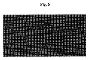
- 238000000635 electron micrograph Methods 0.000 description 6
- 239000002105 nanoparticle Substances 0.000 description 6
- 238000007740 vapor deposition Methods 0.000 description 6
- 238000010586 diagram Methods 0.000 description 5
- 238000010894 electron beam technology Methods 0.000 description 5
- 238000012986 modification Methods 0.000 description 5
- 230000004048 modification Effects 0.000 description 5
- 150000001945 cysteines Chemical group 0.000 description 4
- 238000004518 low pressure chemical vapour deposition Methods 0.000 description 4
- 238000005259 measurement Methods 0.000 description 4
- 238000001020 plasma etching Methods 0.000 description 4
- XLYOFNOQVPJJNP-UHFFFAOYSA-N water Substances O XLYOFNOQVPJJNP-UHFFFAOYSA-N 0.000 description 4
- KFZMGEQAYNKOFK-UHFFFAOYSA-N Isopropanol Chemical compound CC(C)O KFZMGEQAYNKOFK-UHFFFAOYSA-N 0.000 description 3
- OKKJLVBELUTLKV-UHFFFAOYSA-N Methanol Chemical compound OC OKKJLVBELUTLKV-UHFFFAOYSA-N 0.000 description 3
- 108010072866 Prostate-Specific Antigen Proteins 0.000 description 3
- 102100038358 Prostate-specific antigen Human genes 0.000 description 3
- 239000007772 electrode material Substances 0.000 description 3
- 239000007769 metal material Substances 0.000 description 3
- 239000002086 nanomaterial Substances 0.000 description 3
- 238000009279 wet oxidation reaction Methods 0.000 description 3
- CSCPPACGZOOCGX-UHFFFAOYSA-N Acetone Chemical compound CC(C)=O CSCPPACGZOOCGX-UHFFFAOYSA-N 0.000 description 2
- 239000012620 biological material Substances 0.000 description 2
- 239000012472 biological sample Substances 0.000 description 2
- YCIMNLLNPGFGHC-UHFFFAOYSA-N catechol Chemical compound OC1=CC=CC=C1O YCIMNLLNPGFGHC-UHFFFAOYSA-N 0.000 description 2
- 238000006243 chemical reaction Methods 0.000 description 2
- 238000004140 cleaning Methods 0.000 description 2
- 239000013078 crystal Substances 0.000 description 2
- 238000011161 development Methods 0.000 description 2
- 238000004070 electrodeposition Methods 0.000 description 2
- 238000000609 electron-beam lithography Methods 0.000 description 2
- 239000011810 insulating material Substances 0.000 description 2
- 238000001465 metallisation Methods 0.000 description 2
- 239000000523 sample Substances 0.000 description 2
- 125000006850 spacer group Chemical group 0.000 description 2
- 238000005406 washing Methods 0.000 description 2
- 108010032595 Antibody Binding Sites Proteins 0.000 description 1
- 102000053602 DNA Human genes 0.000 description 1
- MYMOFIZGZYHOMD-UHFFFAOYSA-N Dioxygen Chemical compound O=O MYMOFIZGZYHOMD-UHFFFAOYSA-N 0.000 description 1
- PIICEJLVQHRZGT-UHFFFAOYSA-N Ethylenediamine Chemical compound NCCN PIICEJLVQHRZGT-UHFFFAOYSA-N 0.000 description 1
- UFHFLCQGNIYNRP-UHFFFAOYSA-N Hydrogen Chemical compound [H][H] UFHFLCQGNIYNRP-UHFFFAOYSA-N 0.000 description 1
- -1 ITO Substances 0.000 description 1
- 229910021417 amorphous silicon Inorganic materials 0.000 description 1
- QVGXLLKOCUKJST-UHFFFAOYSA-N atomic oxygen Chemical compound [O] QVGXLLKOCUKJST-UHFFFAOYSA-N 0.000 description 1
- 238000003486 chemical etching Methods 0.000 description 1
- 150000001875 compounds Chemical class 0.000 description 1
- 238000010924 continuous production Methods 0.000 description 1
- 238000005520 cutting process Methods 0.000 description 1
- 230000003247 decreasing effect Effects 0.000 description 1
- 229910001882 dioxygen Inorganic materials 0.000 description 1
- 239000012153 distilled water Substances 0.000 description 1
- 238000001647 drug administration Methods 0.000 description 1
- 230000000694 effects Effects 0.000 description 1
- 239000008151 electrolyte solution Substances 0.000 description 1
- 238000000313 electron-beam-induced deposition Methods 0.000 description 1
- 238000011156 evaluation Methods 0.000 description 1
- 238000002474 experimental method Methods 0.000 description 1
- 239000007789 gas Substances 0.000 description 1
- 238000002347 injection Methods 0.000 description 1
- 239000007924 injection Substances 0.000 description 1
- 239000012212 insulator Substances 0.000 description 1
- 238000005442 molecular electronic Methods 0.000 description 1
- 239000002071 nanotube Substances 0.000 description 1
- 239000001301 oxygen Substances 0.000 description 1
- 229910052760 oxygen Inorganic materials 0.000 description 1
- 239000002245 particle Substances 0.000 description 1
- 238000000059 patterning Methods 0.000 description 1
- 229920000642 polymer Polymers 0.000 description 1
- 229920001296 polysiloxane Polymers 0.000 description 1
- 238000011160 research Methods 0.000 description 1
- 239000007787 solid Substances 0.000 description 1
- 125000003396 thiol group Chemical group [H]S* 0.000 description 1
- 238000005019 vapor deposition process Methods 0.000 description 1
Images


Classifications
-
- G—PHYSICS
- G01—MEASURING; TESTING
- G01N—INVESTIGATING OR ANALYSING MATERIALS BY DETERMINING THEIR CHEMICAL OR PHYSICAL PROPERTIES
- G01N33/00—Investigating or analysing materials by specific methods not covered by groups G01N1/00 - G01N31/00
- G01N33/48—Biological material, e.g. blood, urine; Haemocytometers
- G01N33/50—Chemical analysis of biological material, e.g. blood, urine; Testing involving biospecific ligand binding methods; Immunological testing
- G01N33/53—Immunoassay; Biospecific binding assay; Materials therefor
- G01N33/543—Immunoassay; Biospecific binding assay; Materials therefor with an insoluble carrier for immobilising immunochemicals
- G01N33/54366—Apparatus specially adapted for solid-phase testing
- G01N33/54373—Apparatus specially adapted for solid-phase testing involving physiochemical end-point determination, e.g. wave-guides, FETS, gratings
- G01N33/5438—Electrodes
-
- B—PERFORMING OPERATIONS; TRANSPORTING
- B82—NANOTECHNOLOGY
- B82Y—SPECIFIC USES OR APPLICATIONS OF NANOSTRUCTURES; MEASUREMENT OR ANALYSIS OF NANOSTRUCTURES; MANUFACTURE OR TREATMENT OF NANOSTRUCTURES
- B82Y15/00—Nanotechnology for interacting, sensing or actuating, e.g. quantum dots as markers in protein assays or molecular motors
-
- C—CHEMISTRY; METALLURGY
- C30—CRYSTAL GROWTH
- C30B—SINGLE-CRYSTAL GROWTH; UNIDIRECTIONAL SOLIDIFICATION OF EUTECTIC MATERIAL OR UNIDIRECTIONAL DEMIXING OF EUTECTOID MATERIAL; REFINING BY ZONE-MELTING OF MATERIAL; PRODUCTION OF A HOMOGENEOUS POLYCRYSTALLINE MATERIAL WITH DEFINED STRUCTURE; SINGLE CRYSTALS OR HOMOGENEOUS POLYCRYSTALLINE MATERIAL WITH DEFINED STRUCTURE; AFTER-TREATMENT OF SINGLE CRYSTALS OR A HOMOGENEOUS POLYCRYSTALLINE MATERIAL WITH DEFINED STRUCTURE; APPARATUS THEREFOR
- C30B29/00—Single crystals or homogeneous polycrystalline material with defined structure characterised by the material or by their shape
- C30B29/02—Elements
- C30B29/06—Silicon
-
- C—CHEMISTRY; METALLURGY
- C30—CRYSTAL GROWTH
- C30B—SINGLE-CRYSTAL GROWTH; UNIDIRECTIONAL SOLIDIFICATION OF EUTECTIC MATERIAL OR UNIDIRECTIONAL DEMIXING OF EUTECTOID MATERIAL; REFINING BY ZONE-MELTING OF MATERIAL; PRODUCTION OF A HOMOGENEOUS POLYCRYSTALLINE MATERIAL WITH DEFINED STRUCTURE; SINGLE CRYSTALS OR HOMOGENEOUS POLYCRYSTALLINE MATERIAL WITH DEFINED STRUCTURE; AFTER-TREATMENT OF SINGLE CRYSTALS OR A HOMOGENEOUS POLYCRYSTALLINE MATERIAL WITH DEFINED STRUCTURE; APPARATUS THEREFOR
- C30B33/00—After-treatment of single crystals or homogeneous polycrystalline material with defined structure
- C30B33/08—Etching
- C30B33/10—Etching in solutions or melts
-
- G—PHYSICS
- G01—MEASURING; TESTING
- G01N—INVESTIGATING OR ANALYSING MATERIALS BY DETERMINING THEIR CHEMICAL OR PHYSICAL PROPERTIES
- G01N33/00—Investigating or analysing materials by specific methods not covered by groups G01N1/00 - G01N31/00
- G01N33/48—Biological material, e.g. blood, urine; Haemocytometers
- G01N33/50—Chemical analysis of biological material, e.g. blood, urine; Testing involving biospecific ligand binding methods; Immunological testing
- G01N33/53—Immunoassay; Biospecific binding assay; Materials therefor
- G01N33/574—Immunoassay; Biospecific binding assay; Materials therefor for cancer
- G01N33/57407—Specifically defined cancers
- G01N33/57434—Specifically defined cancers of prostate
-
- H—ELECTRICITY
- H01—ELECTRIC ELEMENTS
- H01L—SEMICONDUCTOR DEVICES NOT COVERED BY CLASS H10
- H01L21/00—Processes or apparatus adapted for the manufacture or treatment of semiconductor or solid state devices or of parts thereof
- H01L21/02—Manufacture or treatment of semiconductor devices or of parts thereof
- H01L21/04—Manufacture or treatment of semiconductor devices or of parts thereof the devices having potential barriers, e.g. a PN junction, depletion layer or carrier concentration layer
- H01L21/18—Manufacture or treatment of semiconductor devices or of parts thereof the devices having potential barriers, e.g. a PN junction, depletion layer or carrier concentration layer the devices having semiconductor bodies comprising elements of Group IV of the Periodic Table or AIIIBV compounds with or without impurities, e.g. doping materials
- H01L21/30—Treatment of semiconductor bodies using processes or apparatus not provided for in groups H01L21/20 - H01L21/26
- H01L21/302—Treatment of semiconductor bodies using processes or apparatus not provided for in groups H01L21/20 - H01L21/26 to change their surface-physical characteristics or shape, e.g. etching, polishing, cutting
- H01L21/306—Chemical or electrical treatment, e.g. electrolytic etching
- H01L21/3065—Plasma etching; Reactive-ion etching
- H01L21/30655—Plasma etching; Reactive-ion etching comprising alternated and repeated etching and passivation steps, e.g. Bosch process
Landscapes
- Engineering & Computer Science (AREA)
- Health & Medical Sciences (AREA)
- Chemical & Material Sciences (AREA)
- Life Sciences & Earth Sciences (AREA)
- Immunology (AREA)
- Molecular Biology (AREA)
- Crystallography & Structural Chemistry (AREA)
- Hematology (AREA)
- Urology & Nephrology (AREA)
- Biomedical Technology (AREA)
- General Health & Medical Sciences (AREA)
- Physics & Mathematics (AREA)
- Nanotechnology (AREA)
- Materials Engineering (AREA)
- Metallurgy (AREA)
- Organic Chemistry (AREA)
- General Physics & Mathematics (AREA)
- Food Science & Technology (AREA)
- Medicinal Chemistry (AREA)
- Biotechnology (AREA)
- Analytical Chemistry (AREA)
- Biochemistry (AREA)
- Microbiology (AREA)
- Pathology (AREA)
- Cell Biology (AREA)
- Oncology (AREA)
- Hospice & Palliative Care (AREA)
- Plasma & Fusion (AREA)
- Condensed Matter Physics & Semiconductors (AREA)
- Manufacturing & Machinery (AREA)
- Computer Hardware Design (AREA)
- Microelectronics & Electronic Packaging (AREA)
- Power Engineering (AREA)
- Investigating Or Analyzing Materials By The Use Of Electric Means (AREA)
- Micromachines (AREA)
- Weting (AREA)
- Crystals, And After-Treatments Of Crystals (AREA)
Applications Claiming Priority (3)
| Application Number | Priority Date | Filing Date | Title |
|---|---|---|---|
| KR20050099585 | 2005-10-21 | ||
| KR1020060072981A KR100849384B1 (ko) | 2005-10-21 | 2006-08-02 | 나노갭 및 나노갭 센서의 제조방법 |
| PCT/KR2006/003517 WO2007046582A1 (en) | 2005-10-21 | 2006-09-05 | A method for fabricating nanogap and nanogap sensor |
Publications (2)
| Publication Number | Publication Date |
|---|---|
| JP2009521332A true JP2009521332A (ja) | 2009-06-04 |
| JP2009521332A5 JP2009521332A5 (enExample) | 2009-07-23 |
Family
ID=38178037
Family Applications (1)
| Application Number | Title | Priority Date | Filing Date |
|---|---|---|---|
| JP2008536478A Pending JP2009521332A (ja) | 2005-10-21 | 2006-09-05 | ナノギャップおよびナノギャップセンサの製造方法 |
Country Status (4)
| Country | Link |
|---|---|
| US (1) | US8557567B2 (enExample) |
| JP (1) | JP2009521332A (enExample) |
| KR (1) | KR100849384B1 (enExample) |
| CN (1) | CN101156228B (enExample) |
Cited By (2)
| Publication number | Priority date | Publication date | Assignee | Title |
|---|---|---|---|---|
| WO2011081245A1 (ko) * | 2009-12-29 | 2011-07-07 | 연세대학교 산학협력단 | 수소 센서 및 그 제조방법 |
| JP2022500628A (ja) * | 2018-09-14 | 2022-01-04 | アプライド マテリアルズ インコーポレイテッドApplied Materials, Incorporated | ナノポアを形成する方法およびその結果生じる構造 |
Families Citing this family (30)
| Publication number | Priority date | Publication date | Assignee | Title |
|---|---|---|---|---|
| KR101518733B1 (ko) | 2008-11-27 | 2015-05-11 | 삼성전자주식회사 | 노즐 플레이트 및 그 제조방법 |
| US20110020966A1 (en) * | 2009-07-23 | 2011-01-27 | Canon Kabushiki Kaisha | Method for processing silicon substrate and method for producing substrate for liquid ejecting head |
| KR101130084B1 (ko) * | 2010-04-28 | 2012-03-28 | 연세대학교 산학협력단 | 수소 센서 및 그 제조방법 |
| JP5145463B2 (ja) * | 2009-12-29 | 2013-02-20 | インダストリー−アカデミック コーペレイション ファウンデイション, ヨンセイ ユニバーシティ | 水素センサー及びその製造方法 |
| US9194838B2 (en) | 2010-03-03 | 2015-11-24 | Osaka University | Method and device for identifying nucleotide, and method and device for determining nucleotide sequence of polynucleotide |
| KR20110138657A (ko) * | 2010-06-21 | 2011-12-28 | (주)미코바이오메드 | 표면 플라즈몬 공명 센서 모듈 및 이를 포함한 센싱 시스템 |
| KR101694549B1 (ko) * | 2010-10-21 | 2017-01-09 | (주)미코바이오메드 | 나노 갭 패턴 형성 방법, 나노 갭 패턴을 갖는 바이오 센서 및 바이오 센서 제조 방법 |
| JP6276182B2 (ja) | 2012-08-17 | 2018-02-07 | クオンタムバイオシステムズ株式会社 | 試料の分析方法 |
| KR101878747B1 (ko) | 2012-11-05 | 2018-07-16 | 삼성전자주식회사 | 나노갭 소자 및 이로부터의 신호를 처리하는 방법 |
| KR101927415B1 (ko) | 2012-11-05 | 2019-03-07 | 삼성전자주식회사 | 나노갭 소자 및 이로부터의 신호를 처리하는 방법 |
| JP6282036B2 (ja) | 2012-12-27 | 2018-02-21 | クオンタムバイオシステムズ株式会社 | 物質の移動速度の制御方法および制御装置 |
| WO2015042200A1 (en) * | 2013-09-18 | 2015-03-26 | Osaka University | Biomolecule sequencing devices, systems and methods |
| JP2015077652A (ja) | 2013-10-16 | 2015-04-23 | クオンタムバイオシステムズ株式会社 | ナノギャップ電極およびその製造方法 |
| US10438811B1 (en) | 2014-04-15 | 2019-10-08 | Quantum Biosystems Inc. | Methods for forming nano-gap electrodes for use in nanosensors |
| US9343569B2 (en) | 2014-05-21 | 2016-05-17 | International Business Machines Corporation | Vertical compound semiconductor field effect transistor on a group IV semiconductor substrate |
| CN106796196A (zh) * | 2014-07-11 | 2017-05-31 | 牛津大学科技创新有限公司 | 用于在石墨烯中形成纳米间隙的方法 |
| DE102015211392B4 (de) | 2015-06-19 | 2018-05-24 | Albert-Ludwigs-Universität Freiburg | Elektrodenstruktur und Verfahren zum Herstellen der Elektrodenstruktur und Biosensor-Chip die Elektrodenstruktur umfassend |
| US10247700B2 (en) | 2015-10-30 | 2019-04-02 | International Business Machines Corporation | Embedded noble metal electrodes in microfluidics |
| CA3023577A1 (en) | 2016-04-27 | 2017-11-02 | Quantum Biosystems Inc. | Systems and methods for measurement and sequencing of bio-molecules |
| US11673136B2 (en) * | 2017-04-04 | 2023-06-13 | Arizona Board Of Regents On Behalf Of Arizona State University | Nanopore devices for sensing biomolecules |
| US11740226B2 (en) | 2017-10-13 | 2023-08-29 | Analog Devices International Unlimited Company | Designs and fabrication of nanogap sensors |
| WO2019217600A1 (en) | 2018-05-09 | 2019-11-14 | Stuart Lindsay | Method for electronic detection and quantification of antibodies |
| KR20210045361A (ko) | 2018-05-17 | 2021-04-26 | 레커그니션 어낼러틱스 엘엘씨 | 효소 활성의 직접 전기적 측정을 위한 장치, 시스템 및 방법 |
| BR112021014800A2 (pt) | 2019-01-30 | 2022-01-04 | Univ Arizona State | Circuitos bioeletrônicos, sistemas e métodos para preparação dos mesmos |
| JP2023516167A (ja) | 2020-02-28 | 2023-04-18 | アリゾナ・ボード・オブ・リージェンツ・オン・ビハーフ・オブ・アリゾナ・ステイト・ユニバーシティー | 生体高分子の配列を決定する方法 |
| US12298300B2 (en) | 2020-04-17 | 2025-05-13 | Arizona Board Of Regents On Behalf Of Arizona State University | Single-molecule electronic sequence detector and methods of use |
| CN116018413A (zh) | 2020-05-29 | 2023-04-25 | 代表亚利桑那大学的亚利桑那校董事会 | 具有可编程适配子的生物电子装置 |
| EP4413368A4 (en) * | 2021-10-04 | 2025-11-05 | Tintoria Piana Inc | DIAGNOSTIC SYSTEM AND METHODS FOR USE AND MANUFACTURE THEREOF |
| KR20230060124A (ko) * | 2021-10-27 | 2023-05-04 | 현대자동차주식회사 | 수소 센서 및 수소 센서 제조방법 |
| US20250271389A1 (en) * | 2024-02-28 | 2025-08-28 | Robert Bosch Gmbh | Nucleic acid detection with a nanogap electrical sensor |
Citations (1)
| Publication number | Priority date | Publication date | Assignee | Title |
|---|---|---|---|---|
| JP2005278916A (ja) * | 2004-03-30 | 2005-10-13 | Sanyo Product Co Ltd | 遊技機 |
Family Cites Families (30)
| Publication number | Priority date | Publication date | Assignee | Title |
|---|---|---|---|---|
| US6207369B1 (en) * | 1995-03-10 | 2001-03-27 | Meso Scale Technologies, Llc | Multi-array, multi-specific electrochemiluminescence testing |
| CN1251609A (zh) * | 1997-02-12 | 2000-04-26 | 尤金·Y·查恩 | 分析聚合物的方法和产品 |
| JP3794461B2 (ja) | 1999-04-30 | 2006-07-05 | 日本電信電話株式会社 | 電子結晶あるいは正孔結晶 |
| JP2000315785A (ja) * | 1999-04-30 | 2000-11-14 | Canon Inc | ナノ構造体の製造方法及びナノ構造体デバイス |
| AU5763000A (en) * | 1999-06-22 | 2001-01-09 | President And Fellows Of Harvard College | Molecular and atomic scale evaluation of biopolymers |
| AU3970401A (en) | 1999-11-29 | 2001-06-04 | Trustees Of The University Of Pennsylvania, The | Fabrication of nanometer size gaps on an electrode |
| US7001792B2 (en) | 2000-04-24 | 2006-02-21 | Eagle Research & Development, Llc | Ultra-fast nucleic acid sequencing device and a method for making and using the same |
| US8232582B2 (en) * | 2000-04-24 | 2012-07-31 | Life Technologies Corporation | Ultra-fast nucleic acid sequencing device and a method for making and using the same |
| US7291284B2 (en) * | 2000-05-26 | 2007-11-06 | Northwestern University | Fabrication of sub-50 nm solid-state nanostructures based on nanolithography |
| US7148058B2 (en) * | 2000-06-05 | 2006-12-12 | Chiron Corporation | Protein microarrays on mirrored surfaces for performing proteomic analyses |
| KR20030052665A (ko) * | 2001-12-21 | 2003-06-27 | 주식회사 하이닉스반도체 | 나노 크기의 스페이스 패턴 형성 방법 |
| DE10204690A1 (de) | 2002-02-06 | 2003-08-07 | Clariant Gmbh | Verfahren zur Herstellung synergistischer Stabilisatormischungen |
| US7005264B2 (en) * | 2002-05-20 | 2006-02-28 | Intel Corporation | Method and apparatus for nucleic acid sequencing and identification |
| EP1366860B1 (en) | 2002-05-28 | 2005-03-23 | Asia Pacific Microsystem, Inc. | Non-destructive method for measuring the thickness of a bonded wafer |
| EP1592641B1 (en) | 2003-02-03 | 2018-03-07 | President and Fellows of Harvard College | Controlled fabrication of gaps in electrically conducting structures |
| JP3787630B2 (ja) * | 2003-02-14 | 2006-06-21 | 独立行政法人情報通信研究機構 | ナノギャップ電極の製造方法 |
| NL1022855C2 (nl) | 2003-03-05 | 2004-09-07 | Univ Delft Tech | Werkwijze en inrichting voor het gecontroleerd vervaardigen van openingen op nanometerschaal. |
| US7172917B2 (en) * | 2003-04-17 | 2007-02-06 | Robert Bosch Gmbh | Method of making a nanogap for variable capacitive elements, and device having a nanogap |
| JP3864229B2 (ja) * | 2003-08-29 | 2006-12-27 | 独立行政法人産業技術総合研究所 | ナノギャップ電極の製造方法及び該方法により製造されたナノギャップ電極を有する素子 |
| WO2005069001A1 (ja) * | 2003-09-25 | 2005-07-28 | Toyama Prefecture | マイクロウェルアレイチップ及びその製造方法 |
| US7851203B2 (en) * | 2003-10-01 | 2010-12-14 | Lawrence Livermore National Security, Llc | Functionalized apertures for the detection of chemical and biological materials |
| KR100561908B1 (ko) | 2003-12-26 | 2006-03-20 | 한국전자통신연구원 | 센서 구조체 및 그 제조방법 |
| US20080025875A1 (en) * | 2004-09-29 | 2008-01-31 | Martin Charles R | Chemical, Particle, and Biosensing with Nanotechnology |
| US20060073489A1 (en) * | 2004-10-05 | 2006-04-06 | Gangqiang Li | Nanopore separation devices and methods of using same |
| KR100679704B1 (ko) * | 2005-01-10 | 2007-02-06 | 한국과학기술원 | 분자소자와 바이오 센서를 위한 나노갭 또는 나노 전계효과 트랜지스터 제작방법 |
| US7947485B2 (en) * | 2005-06-03 | 2011-05-24 | Hewlett-Packard Development Company, L.P. | Method and apparatus for molecular analysis using nanoelectronic circuits |
| US7410762B1 (en) * | 2005-06-27 | 2008-08-12 | Sandia Corporation | Method for detecting biomolecules |
| TW200700038A (en) * | 2005-06-27 | 2007-01-01 | Chieh Shang Co Ltd | Inflatable air cushion |
| US8860438B2 (en) * | 2009-05-11 | 2014-10-14 | Clemson University Research Foundation | Electrical double layer capacitive devices and methods of using same for sequencing polymers and detecting analytes |
| KR200457140Y1 (ko) | 2010-01-22 | 2011-12-06 | (주)파트론정밀 | 전자기기용 플랙시블 플레이트 케이블 커넥터 |
-
2006
- 2006-08-02 KR KR1020060072981A patent/KR100849384B1/ko not_active Expired - Fee Related
- 2006-09-05 JP JP2008536478A patent/JP2009521332A/ja active Pending
- 2006-09-05 CN CN200680011497.0A patent/CN101156228B/zh not_active Expired - Fee Related
- 2006-09-05 US US11/887,978 patent/US8557567B2/en not_active Expired - Fee Related
Patent Citations (1)
| Publication number | Priority date | Publication date | Assignee | Title |
|---|---|---|---|---|
| JP2005278916A (ja) * | 2004-03-30 | 2005-10-13 | Sanyo Product Co Ltd | 遊技機 |
Non-Patent Citations (1)
| Title |
|---|
| YANG-KYU CHOI: "Sublithographic nanofabrication technology for nanocatalystsand DNA chips", J. VAC. SCI. TECHNOL. B,, vol. Vol. 21, No. 6,, JPN6011058407, 2003, pages 2951 - 2955, ISSN: 0002063554 * |
Cited By (4)
| Publication number | Priority date | Publication date | Assignee | Title |
|---|---|---|---|---|
| WO2011081245A1 (ko) * | 2009-12-29 | 2011-07-07 | 연세대학교 산학협력단 | 수소 센서 및 그 제조방법 |
| KR101067557B1 (ko) | 2009-12-29 | 2011-09-27 | 연세대학교 산학협력단 | 수소 센서 및 그 제조방법 |
| JP2022500628A (ja) * | 2018-09-14 | 2022-01-04 | アプライド マテリアルズ インコーポレイテッドApplied Materials, Incorporated | ナノポアを形成する方法およびその結果生じる構造 |
| JP7190558B2 (ja) | 2018-09-14 | 2022-12-15 | アプライド マテリアルズ インコーポレイテッド | ナノポアを形成する方法およびその結果生じる構造 |
Also Published As
| Publication number | Publication date |
|---|---|
| CN101156228B (zh) | 2013-01-30 |
| KR20070043591A (ko) | 2007-04-25 |
| US8557567B2 (en) | 2013-10-15 |
| KR100849384B1 (ko) | 2008-07-31 |
| US20090215156A1 (en) | 2009-08-27 |
| CN101156228A (zh) | 2008-04-02 |
Similar Documents
| Publication | Publication Date | Title |
|---|---|---|
| JP2009521332A (ja) | ナノギャップおよびナノギャップセンサの製造方法 | |
| US7824620B2 (en) | Nano- and micro-scale structures: methods, devices and applications thereof | |
| US20200393440A1 (en) | Method, apparatus and system for single-molecule polymerase biosensor with transition metal nanobridge | |
| TWI424160B (zh) | 結合矽奈米線閘極二極體之感測元件、製造方法及其檢測系統 | |
| US8241939B2 (en) | Semiconductor nanowire sensor device and method for manufacturing the same | |
| JP2011518311A (ja) | ナノセンサプラットフォームを使用および構築する方法 | |
| JP2006503277A (ja) | 分子エレクトロニクスと分子エレクトロニクスに基づいたバイオセンサーデバイスのための半導体装置及びその製造方法 | |
| US12352723B2 (en) | Biofunctionalized three-dimensional (3D) graphene-based field-effect transistor (FET) sensor | |
| US20210396708A1 (en) | Methods for detecting analytes using a graphene-based biological field-effect transistor | |
| Danielson et al. | Gas-phase synthesis for label-free biosensors: zinc-oxide nanowires functionalized with gold nanoparticles | |
| KR101489154B1 (ko) | 잔류응력을 이용한 나노갭 센서의 제조방법 및 이에 의해 제조되는 나노갭 센서 | |
| US20160252506A1 (en) | Silicon nanowire-based sensor arrays | |
| Sinha et al. | Selective, ultra-sensitive, and rapid detection of serotonin by optimized ZnO nanorod FET biosensor | |
| CN115901888B (zh) | 一种利用二维平面纳米导电材料侧面的电化学一维纳米电极及其制备方法与应用 | |
| WO2008021614A2 (en) | Coded particle arrays for high throughput analyte analysis | |
| Samà et al. | Electron beam lithography for contacting single nanowires on non-flat suspended substrates | |
| Kumar et al. | Time-dependent pH sensing phenomena using CdSe/ZnS quantum dots in EIS structure | |
| US11988629B2 (en) | Method of manufacturing a graphene-based biological field-effect transistor | |
| US20230038666A1 (en) | Nanobridge biosensor and memory array | |
| JPWO2007086268A1 (ja) | 微小電極およびその製造方法 | |
| Carrara et al. | Methods to fabricate nanocontacts for electrical addressing of single molecules | |
| Adam et al. | Novel in-house fabrication of nano lab-on-chip devices | |
| Gao et al. | On-chip suspended gold nanowire electrode with a rough surface: Fabrication and electrochemical properties | |
| EP1938364A1 (en) | A method for fabricating nanogap and nanogap sensor | |
| Łaszcz et al. | Fabrication of electrochemical nanoelectrode for sensor application using focused ion beam technology |
Legal Events
| Date | Code | Title | Description |
|---|---|---|---|
| A521 | Request for written amendment filed |
Free format text: JAPANESE INTERMEDIATE CODE: A523 Effective date: 20090513 |
|
| A711 | Notification of change in applicant |
Free format text: JAPANESE INTERMEDIATE CODE: A711 Effective date: 20100802 |
|
| A521 | Request for written amendment filed |
Free format text: JAPANESE INTERMEDIATE CODE: A821 Effective date: 20100802 |
|
| A131 | Notification of reasons for refusal |
Free format text: JAPANESE INTERMEDIATE CODE: A131 Effective date: 20111108 |
|
| A02 | Decision of refusal |
Free format text: JAPANESE INTERMEDIATE CODE: A02 Effective date: 20120417 |