JP2009521332A - Manufacturing method of nanogap and nanogap sensor - Google Patents
Manufacturing method of nanogap and nanogap sensor Download PDFInfo
- Publication number
- JP2009521332A JP2009521332A JP2008536478A JP2008536478A JP2009521332A JP 2009521332 A JP2009521332 A JP 2009521332A JP 2008536478 A JP2008536478 A JP 2008536478A JP 2008536478 A JP2008536478 A JP 2008536478A JP 2009521332 A JP2009521332 A JP 2009521332A
- Authority
- JP
- Japan
- Prior art keywords
- nanogap
- substrate
- etching
- sensor
- mask material
- Prior art date
- Legal status (The legal status is an assumption and is not a legal conclusion. Google has not performed a legal analysis and makes no representation as to the accuracy of the status listed.)
- Pending
Links
- 238000004519 manufacturing process Methods 0.000 title claims abstract description 41
- 239000000758 substrate Substances 0.000 claims abstract description 88
- 238000005530 etching Methods 0.000 claims abstract description 68
- 238000000034 method Methods 0.000 claims description 111
- XUIMIQQOPSSXEZ-UHFFFAOYSA-N Silicon Chemical compound [Si] XUIMIQQOPSSXEZ-UHFFFAOYSA-N 0.000 claims description 62
- 229910052710 silicon Inorganic materials 0.000 claims description 60
- 239000010703 silicon Substances 0.000 claims description 60
- 239000000463 material Substances 0.000 claims description 50
- VYPSYNLAJGMNEJ-UHFFFAOYSA-N Silicium dioxide Chemical compound O=[Si]=O VYPSYNLAJGMNEJ-UHFFFAOYSA-N 0.000 claims description 26
- 229920002120 photoresistant polymer Polymers 0.000 claims description 25
- 230000003647 oxidation Effects 0.000 claims description 21
- 238000007254 oxidation reaction Methods 0.000 claims description 21
- 229910052751 metal Inorganic materials 0.000 claims description 18
- 239000002184 metal Substances 0.000 claims description 18
- 238000001039 wet etching Methods 0.000 claims description 15
- 239000012491 analyte Substances 0.000 claims description 14
- 239000000126 substance Substances 0.000 claims description 14
- 229910004298 SiO 2 Inorganic materials 0.000 claims description 11
- 238000000151 deposition Methods 0.000 claims description 11
- 239000010931 gold Substances 0.000 claims description 11
- PCHJSUWPFVWCPO-UHFFFAOYSA-N gold Chemical compound [Au] PCHJSUWPFVWCPO-UHFFFAOYSA-N 0.000 claims description 10
- 229910052737 gold Inorganic materials 0.000 claims description 10
- 238000002161 passivation Methods 0.000 claims description 10
- BASFCYQUMIYNBI-UHFFFAOYSA-N platinum Chemical compound [Pt] BASFCYQUMIYNBI-UHFFFAOYSA-N 0.000 claims description 10
- WGTYBPLFGIVFAS-UHFFFAOYSA-M tetramethylammonium hydroxide Chemical compound [OH-].C[N+](C)(C)C WGTYBPLFGIVFAS-UHFFFAOYSA-M 0.000 claims description 10
- 235000018417 cysteine Nutrition 0.000 claims description 9
- KDLHZDBZIXYQEI-UHFFFAOYSA-N Palladium Chemical compound [Pd] KDLHZDBZIXYQEI-UHFFFAOYSA-N 0.000 claims description 8
- 101710120037 Toxin CcdB Proteins 0.000 claims description 8
- 235000018102 proteins Nutrition 0.000 claims description 8
- 108090000623 proteins and genes Proteins 0.000 claims description 8
- 102000004169 proteins and genes Human genes 0.000 claims description 8
- 239000000427 antigen Substances 0.000 claims description 7
- 102000036639 antigens Human genes 0.000 claims description 6
- 108091007433 antigens Proteins 0.000 claims description 6
- 230000015572 biosynthetic process Effects 0.000 claims description 6
- 238000001312 dry etching Methods 0.000 claims description 6
- RYGMFSIKBFXOCR-UHFFFAOYSA-N Copper Chemical compound [Cu] RYGMFSIKBFXOCR-UHFFFAOYSA-N 0.000 claims description 5
- 238000004458 analytical method Methods 0.000 claims description 5
- 239000011651 chromium Substances 0.000 claims description 5
- 229910052802 copper Inorganic materials 0.000 claims description 5
- 239000010949 copper Substances 0.000 claims description 5
- 229910052697 platinum Inorganic materials 0.000 claims description 5
- VYZAMTAEIAYCRO-UHFFFAOYSA-N Chromium Chemical compound [Cr] VYZAMTAEIAYCRO-UHFFFAOYSA-N 0.000 claims description 4
- BQCADISMDOOEFD-UHFFFAOYSA-N Silver Chemical compound [Ag] BQCADISMDOOEFD-UHFFFAOYSA-N 0.000 claims description 4
- RTAQQCXQSZGOHL-UHFFFAOYSA-N Titanium Chemical compound [Ti] RTAQQCXQSZGOHL-UHFFFAOYSA-N 0.000 claims description 4
- 229910052782 aluminium Inorganic materials 0.000 claims description 4
- XAGFODPZIPBFFR-UHFFFAOYSA-N aluminium Chemical compound [Al] XAGFODPZIPBFFR-UHFFFAOYSA-N 0.000 claims description 4
- 229910052804 chromium Inorganic materials 0.000 claims description 4
- XUJNEKJLAYXESH-UHFFFAOYSA-N cysteine Natural products SCC(N)C(O)=O XUJNEKJLAYXESH-UHFFFAOYSA-N 0.000 claims description 4
- 238000005566 electron beam evaporation Methods 0.000 claims description 4
- 229910052763 palladium Inorganic materials 0.000 claims description 4
- 229910052814 silicon oxide Inorganic materials 0.000 claims description 4
- 229910052709 silver Inorganic materials 0.000 claims description 4
- 239000004332 silver Substances 0.000 claims description 4
- 229910052719 titanium Inorganic materials 0.000 claims description 4
- 239000010936 titanium Substances 0.000 claims description 4
- 229910018072 Al 2 O 3 Inorganic materials 0.000 claims description 3
- 229910052581 Si3N4 Inorganic materials 0.000 claims description 3
- 229910045601 alloy Inorganic materials 0.000 claims description 3
- 239000000956 alloy Substances 0.000 claims description 3
- 239000000919 ceramic Substances 0.000 claims description 3
- 125000000151 cysteine group Chemical group N[C@@H](CS)C(=O)* 0.000 claims description 3
- 239000011521 glass Substances 0.000 claims description 3
- HQVNEWCFYHHQES-UHFFFAOYSA-N silicon nitride Chemical compound N12[Si]34N5[Si]62N3[Si]51N64 HQVNEWCFYHHQES-UHFFFAOYSA-N 0.000 claims description 3
- 238000000992 sputter etching Methods 0.000 claims description 3
- AMGQUBHHOARCQH-UHFFFAOYSA-N indium;oxotin Chemical compound [In].[Sn]=O AMGQUBHHOARCQH-UHFFFAOYSA-N 0.000 claims description 2
- 229910021421 monocrystalline silicon Inorganic materials 0.000 claims description 2
- 102000004190 Enzymes Human genes 0.000 claims 2
- 108090000790 Enzymes Proteins 0.000 claims 2
- 239000012634 fragment Substances 0.000 claims 2
- 206010060862 Prostate cancer Diseases 0.000 claims 1
- 208000000236 Prostatic Neoplasms Diseases 0.000 claims 1
- 230000004071 biological effect Effects 0.000 claims 1
- 238000002372 labelling Methods 0.000 claims 1
- 239000002773 nucleotide Substances 0.000 claims 1
- 125000003729 nucleotide group Chemical group 0.000 claims 1
- 239000004065 semiconductor Substances 0.000 abstract description 10
- 238000005516 engineering process Methods 0.000 abstract description 6
- KWYUFKZDYYNOTN-UHFFFAOYSA-M Potassium hydroxide Chemical compound [OH-].[K+] KWYUFKZDYYNOTN-UHFFFAOYSA-M 0.000 description 45
- 239000000377 silicon dioxide Substances 0.000 description 11
- 235000012239 silicon dioxide Nutrition 0.000 description 11
- 239000000243 solution Substances 0.000 description 8
- 108020004414 DNA Proteins 0.000 description 7
- 238000000635 electron micrograph Methods 0.000 description 6
- 239000002105 nanoparticle Substances 0.000 description 6
- 238000007740 vapor deposition Methods 0.000 description 6
- 238000010586 diagram Methods 0.000 description 5
- 238000010894 electron beam technology Methods 0.000 description 5
- 238000012986 modification Methods 0.000 description 5
- 230000004048 modification Effects 0.000 description 5
- 150000001945 cysteines Chemical group 0.000 description 4
- 238000004518 low pressure chemical vapour deposition Methods 0.000 description 4
- 238000005259 measurement Methods 0.000 description 4
- 238000001020 plasma etching Methods 0.000 description 4
- XLYOFNOQVPJJNP-UHFFFAOYSA-N water Substances O XLYOFNOQVPJJNP-UHFFFAOYSA-N 0.000 description 4
- KFZMGEQAYNKOFK-UHFFFAOYSA-N Isopropanol Chemical compound CC(C)O KFZMGEQAYNKOFK-UHFFFAOYSA-N 0.000 description 3
- OKKJLVBELUTLKV-UHFFFAOYSA-N Methanol Chemical compound OC OKKJLVBELUTLKV-UHFFFAOYSA-N 0.000 description 3
- 108010072866 Prostate-Specific Antigen Proteins 0.000 description 3
- 102100038358 Prostate-specific antigen Human genes 0.000 description 3
- 239000007772 electrode material Substances 0.000 description 3
- 239000007769 metal material Substances 0.000 description 3
- 239000002086 nanomaterial Substances 0.000 description 3
- 238000009279 wet oxidation reaction Methods 0.000 description 3
- CSCPPACGZOOCGX-UHFFFAOYSA-N Acetone Chemical compound CC(C)=O CSCPPACGZOOCGX-UHFFFAOYSA-N 0.000 description 2
- 239000012620 biological material Substances 0.000 description 2
- 239000012472 biological sample Substances 0.000 description 2
- YCIMNLLNPGFGHC-UHFFFAOYSA-N catechol Chemical compound OC1=CC=CC=C1O YCIMNLLNPGFGHC-UHFFFAOYSA-N 0.000 description 2
- 238000006243 chemical reaction Methods 0.000 description 2
- 238000004140 cleaning Methods 0.000 description 2
- 239000013078 crystal Substances 0.000 description 2
- 238000011161 development Methods 0.000 description 2
- 238000004070 electrodeposition Methods 0.000 description 2
- 238000000609 electron-beam lithography Methods 0.000 description 2
- 239000011810 insulating material Substances 0.000 description 2
- 238000001465 metallisation Methods 0.000 description 2
- 239000000523 sample Substances 0.000 description 2
- 125000006850 spacer group Chemical group 0.000 description 2
- 238000005406 washing Methods 0.000 description 2
- 108010032595 Antibody Binding Sites Proteins 0.000 description 1
- 102000053602 DNA Human genes 0.000 description 1
- MYMOFIZGZYHOMD-UHFFFAOYSA-N Dioxygen Chemical compound O=O MYMOFIZGZYHOMD-UHFFFAOYSA-N 0.000 description 1
- PIICEJLVQHRZGT-UHFFFAOYSA-N Ethylenediamine Chemical compound NCCN PIICEJLVQHRZGT-UHFFFAOYSA-N 0.000 description 1
- UFHFLCQGNIYNRP-UHFFFAOYSA-N Hydrogen Chemical compound [H][H] UFHFLCQGNIYNRP-UHFFFAOYSA-N 0.000 description 1
- -1 ITO Substances 0.000 description 1
- 229910021417 amorphous silicon Inorganic materials 0.000 description 1
- QVGXLLKOCUKJST-UHFFFAOYSA-N atomic oxygen Chemical compound [O] QVGXLLKOCUKJST-UHFFFAOYSA-N 0.000 description 1
- 238000003486 chemical etching Methods 0.000 description 1
- 150000001875 compounds Chemical class 0.000 description 1
- 238000010924 continuous production Methods 0.000 description 1
- 238000005520 cutting process Methods 0.000 description 1
- 230000003247 decreasing effect Effects 0.000 description 1
- 229910001882 dioxygen Inorganic materials 0.000 description 1
- 239000012153 distilled water Substances 0.000 description 1
- 238000001647 drug administration Methods 0.000 description 1
- 230000000694 effects Effects 0.000 description 1
- 239000008151 electrolyte solution Substances 0.000 description 1
- 238000000313 electron-beam-induced deposition Methods 0.000 description 1
- 238000011156 evaluation Methods 0.000 description 1
- 238000002474 experimental method Methods 0.000 description 1
- 239000007789 gas Substances 0.000 description 1
- 238000002347 injection Methods 0.000 description 1
- 239000007924 injection Substances 0.000 description 1
- 239000012212 insulator Substances 0.000 description 1
- 238000005442 molecular electronic Methods 0.000 description 1
- 239000002071 nanotube Substances 0.000 description 1
- 239000001301 oxygen Substances 0.000 description 1
- 229910052760 oxygen Inorganic materials 0.000 description 1
- 239000002245 particle Substances 0.000 description 1
- 238000000059 patterning Methods 0.000 description 1
- 229920000642 polymer Polymers 0.000 description 1
- 229920001296 polysiloxane Polymers 0.000 description 1
- 238000011160 research Methods 0.000 description 1
- 239000007787 solid Substances 0.000 description 1
- 125000003396 thiol group Chemical group [H]S* 0.000 description 1
- 238000005019 vapor deposition process Methods 0.000 description 1
Images


Classifications
-
- G—PHYSICS
- G01—MEASURING; TESTING
- G01N—INVESTIGATING OR ANALYSING MATERIALS BY DETERMINING THEIR CHEMICAL OR PHYSICAL PROPERTIES
- G01N33/00—Investigating or analysing materials by specific methods not covered by groups G01N1/00 - G01N31/00
- G01N33/48—Biological material, e.g. blood, urine; Haemocytometers
- G01N33/50—Chemical analysis of biological material, e.g. blood, urine; Testing involving biospecific ligand binding methods; Immunological testing
- G01N33/53—Immunoassay; Biospecific binding assay; Materials therefor
- G01N33/543—Immunoassay; Biospecific binding assay; Materials therefor with an insoluble carrier for immobilising immunochemicals
- G01N33/54366—Apparatus specially adapted for solid-phase testing
- G01N33/54373—Apparatus specially adapted for solid-phase testing involving physiochemical end-point determination, e.g. wave-guides, FETS, gratings
- G01N33/5438—Electrodes
-
- B—PERFORMING OPERATIONS; TRANSPORTING
- B82—NANOTECHNOLOGY
- B82Y—SPECIFIC USES OR APPLICATIONS OF NANOSTRUCTURES; MEASUREMENT OR ANALYSIS OF NANOSTRUCTURES; MANUFACTURE OR TREATMENT OF NANOSTRUCTURES
- B82Y15/00—Nanotechnology for interacting, sensing or actuating, e.g. quantum dots as markers in protein assays or molecular motors
-
- C—CHEMISTRY; METALLURGY
- C30—CRYSTAL GROWTH
- C30B—SINGLE-CRYSTAL GROWTH; UNIDIRECTIONAL SOLIDIFICATION OF EUTECTIC MATERIAL OR UNIDIRECTIONAL DEMIXING OF EUTECTOID MATERIAL; REFINING BY ZONE-MELTING OF MATERIAL; PRODUCTION OF A HOMOGENEOUS POLYCRYSTALLINE MATERIAL WITH DEFINED STRUCTURE; SINGLE CRYSTALS OR HOMOGENEOUS POLYCRYSTALLINE MATERIAL WITH DEFINED STRUCTURE; AFTER-TREATMENT OF SINGLE CRYSTALS OR A HOMOGENEOUS POLYCRYSTALLINE MATERIAL WITH DEFINED STRUCTURE; APPARATUS THEREFOR
- C30B29/00—Single crystals or homogeneous polycrystalline material with defined structure characterised by the material or by their shape
- C30B29/02—Elements
- C30B29/06—Silicon
-
- C—CHEMISTRY; METALLURGY
- C30—CRYSTAL GROWTH
- C30B—SINGLE-CRYSTAL GROWTH; UNIDIRECTIONAL SOLIDIFICATION OF EUTECTIC MATERIAL OR UNIDIRECTIONAL DEMIXING OF EUTECTOID MATERIAL; REFINING BY ZONE-MELTING OF MATERIAL; PRODUCTION OF A HOMOGENEOUS POLYCRYSTALLINE MATERIAL WITH DEFINED STRUCTURE; SINGLE CRYSTALS OR HOMOGENEOUS POLYCRYSTALLINE MATERIAL WITH DEFINED STRUCTURE; AFTER-TREATMENT OF SINGLE CRYSTALS OR A HOMOGENEOUS POLYCRYSTALLINE MATERIAL WITH DEFINED STRUCTURE; APPARATUS THEREFOR
- C30B33/00—After-treatment of single crystals or homogeneous polycrystalline material with defined structure
- C30B33/08—Etching
- C30B33/10—Etching in solutions or melts
-
- G—PHYSICS
- G01—MEASURING; TESTING
- G01N—INVESTIGATING OR ANALYSING MATERIALS BY DETERMINING THEIR CHEMICAL OR PHYSICAL PROPERTIES
- G01N33/00—Investigating or analysing materials by specific methods not covered by groups G01N1/00 - G01N31/00
- G01N33/48—Biological material, e.g. blood, urine; Haemocytometers
- G01N33/50—Chemical analysis of biological material, e.g. blood, urine; Testing involving biospecific ligand binding methods; Immunological testing
- G01N33/53—Immunoassay; Biospecific binding assay; Materials therefor
- G01N33/574—Immunoassay; Biospecific binding assay; Materials therefor for cancer
- G01N33/57407—Specifically defined cancers
- G01N33/57434—Specifically defined cancers of prostate
-
- H—ELECTRICITY
- H01—ELECTRIC ELEMENTS
- H01L—SEMICONDUCTOR DEVICES NOT COVERED BY CLASS H10
- H01L21/00—Processes or apparatus adapted for the manufacture or treatment of semiconductor or solid state devices or of parts thereof
- H01L21/02—Manufacture or treatment of semiconductor devices or of parts thereof
- H01L21/04—Manufacture or treatment of semiconductor devices or of parts thereof the devices having potential barriers, e.g. a PN junction, depletion layer or carrier concentration layer
- H01L21/18—Manufacture or treatment of semiconductor devices or of parts thereof the devices having potential barriers, e.g. a PN junction, depletion layer or carrier concentration layer the devices having semiconductor bodies comprising elements of Group IV of the Periodic Table or AIIIBV compounds with or without impurities, e.g. doping materials
- H01L21/30—Treatment of semiconductor bodies using processes or apparatus not provided for in groups H01L21/20 - H01L21/26
- H01L21/302—Treatment of semiconductor bodies using processes or apparatus not provided for in groups H01L21/20 - H01L21/26 to change their surface-physical characteristics or shape, e.g. etching, polishing, cutting
- H01L21/306—Chemical or electrical treatment, e.g. electrolytic etching
- H01L21/3065—Plasma etching; Reactive-ion etching
- H01L21/30655—Plasma etching; Reactive-ion etching comprising alternated and repeated etching and passivation steps, e.g. Bosch process
Landscapes
- Engineering & Computer Science (AREA)
- Health & Medical Sciences (AREA)
- Chemical & Material Sciences (AREA)
- Life Sciences & Earth Sciences (AREA)
- Immunology (AREA)
- Molecular Biology (AREA)
- Crystallography & Structural Chemistry (AREA)
- Hematology (AREA)
- Urology & Nephrology (AREA)
- Biomedical Technology (AREA)
- General Health & Medical Sciences (AREA)
- Physics & Mathematics (AREA)
- Nanotechnology (AREA)
- Materials Engineering (AREA)
- Metallurgy (AREA)
- Organic Chemistry (AREA)
- General Physics & Mathematics (AREA)
- Food Science & Technology (AREA)
- Medicinal Chemistry (AREA)
- Biotechnology (AREA)
- Analytical Chemistry (AREA)
- Biochemistry (AREA)
- Microbiology (AREA)
- Pathology (AREA)
- Cell Biology (AREA)
- Oncology (AREA)
- Hospice & Palliative Care (AREA)
- Plasma & Fusion (AREA)
- Condensed Matter Physics & Semiconductors (AREA)
- Manufacturing & Machinery (AREA)
- Computer Hardware Design (AREA)
- Microelectronics & Electronic Packaging (AREA)
- Power Engineering (AREA)
- Investigating Or Analyzing Materials By The Use Of Electric Means (AREA)
- Micromachines (AREA)
- Weting (AREA)
- Crystals, And After-Treatments Of Crystals (AREA)
Abstract
【課題】半導体製造工程技術を用いて、高価の装備を使用することなく簡単且つ容易にナノギャップおよびナノギャップセンサを量産することが可能なナノギャップおよびナノギャップセンサの製造方法の提供。
【解決手段】基板に対して異方性エッチングを行うことを含む、ナノギャップ製造方法を提供する。Provided is a method of manufacturing a nanogap and a nanogap sensor that can easily and easily mass-produce a nanogap and a nanogap sensor without using expensive equipment by using a semiconductor manufacturing process technology.
A method of manufacturing a nanogap comprising performing anisotropic etching on a substrate is provided.
Description
本発明は、ナノギャップおよびナノギャップセンサの製造方法に係り、具体的には、半導体製造工程を用いて簡単かつ低コストでナノギャップの位置と幅を容易に調節することが可能なナノギャップおよびナノギャップセンサの製造方法に関する。 The present invention relates to a method for manufacturing a nanogap and a nanogap sensor, and more specifically, a nanogap capable of easily adjusting the position and width of a nanogap at a low cost using a semiconductor manufacturing process. The present invention relates to a method for manufacturing a nanogap sensor.
一般に、ナノギャップは、電極への応用が可能なので、ナノサイズ構造物の電気的特性を研究し、或いは極微量の化学物質または生体物質を感知するセンサとして活用することが可能である。特に、分子水準において電気的特性の変化などを測定するためにはナノギャップが必須的である。 In general, the nanogap can be applied to an electrode, so that it can be used as a sensor for studying electrical characteristics of a nano-sized structure or detecting a very small amount of chemical or biological substance. In particular, a nanogap is essential for measuring changes in electrical properties at the molecular level.
最近、ナノギャップを製造する方法として、エレクトロマイグレーション(electromigration)現象を用いて金属電線の特定の位置にギャップを生成させる方法(非特許文献1)、電子ビームリソグラフィー(electron-beam lithography)を用いる方法(非特許文献2)、比較的大きいギャップを作った後、電気化学蒸着法(electrochemical deposition)でギャップの大きさを減らす方法(非特許文献3)、およびシャドーマスク(shadow mask)を用いた方法(特許文献1)などが提案された。 Recently, as a method of manufacturing a nanogap, a method of generating a gap at a specific position of a metal wire using an electromigration phenomenon (non-patent document 1), a method of using electron-beam lithography (Non-patent document 2) A method of reducing the size of a gap by electrochemical deposition after making a relatively large gap (non-patent document 3), and a method using a shadow mask (Patent document 1) etc. were proposed.
ところが、数十〜数百ナノメートルの線幅を持つ金属電線を作って電流を流し、金属電線の内部において原子が電子流れの影響を受けて漸次移動するエレクトロマイグレーション現象を用いて金属電線の特定の部分を断ち切ることにより、数ナノメートルの幅を持つナノギャップを形成するエレクトロマイグレーション現象を利用する方法は、ナノギャップの位置と大きさを正確に制御することが難しい。 However, a metal wire having a line width of several tens to several hundreds of nanometers is made to pass a current, and the metal wire is identified using an electromigration phenomenon in which atoms gradually move under the influence of an electron flow inside the metal wire. It is difficult to accurately control the position and size of the nanogap in the method using the electromigration phenomenon in which a nanogap having a width of several nanometers is formed by cutting off the portion of the nanogap.
また、電子ビームによって直接パターニングを行う電子ビームリソグラフィーを用いた方法は、精密なナノギャップを得ることはできるが、コストが過大になって大量でナノギャップを製作することが難しい。 In addition, a method using electron beam lithography in which direct patterning is performed by an electron beam can obtain a precise nanogap, but the cost is excessive and it is difficult to manufacture a nanogap in a large amount.
また、特許文献2では、第1電極の一側にスペーサを位置させた後、第2電極を形成し、その後スペーサを除去してナノギャップの電極を形成する方法を開示している。ところが、これは、工程が煩わしく、ナノギャップの幅調節が難しく、多数のナノギャップ電極素子を同時に形成することが不可能であるという欠点がある。 Patent Document 2 discloses a method of forming a nanogap electrode by forming a second electrode after positioning a spacer on one side of the first electrode and then removing the spacer. However, this has the disadvantages that the process is cumbersome, it is difficult to adjust the width of the nanogap, and it is impossible to simultaneously form a large number of nanogap electrode elements.
また、特定の基板上に比較的大きいギャップで離れている金属電極を形成し、金属電極パターンに電気端子を連結し、基板全体を特定の電解液に浸した後、電圧を印加し、金属電極パターンの表面に電極物質層を蒸着して電極物質層を厚くすることにより、ギャップの幅を益々減少させてナノギャップを形成する電気化学蒸着法を用いた方法は、工程が複雑であり、ナノギャップの大きさの調節が難しい。 In addition, a metal electrode that is separated by a relatively large gap is formed on a specific substrate, an electric terminal is connected to the metal electrode pattern, the entire substrate is immersed in a specific electrolytic solution, and then a voltage is applied to the metal electrode. The method using the electrochemical deposition method in which the gap width is further reduced to form the nano gap by increasing the thickness of the electrode material layer by depositing the electrode material layer on the surface of the pattern is complicated, and the process is complicated. It is difficult to adjust the gap size.
また、ナノチューブなどのナノ構造物を載せた後、金属物質を蒸着させて、ナノ構造物が持っている大きさに相当するだけのナノギャップを生成するシャドーマスクを用いた方法は、生成されるナノギャップの大きさが使用されるナノ構造物の大きさに依存し、所望の位置にナノギャップを生成することが難しい。このように既存の半導体工程技術などを用いる場合、経済的且つ効率的にナノギャップを大量生産することが難しく、その結果、ナノメートル水準の大きさを持つ物質、例えば単一分子、ナノパーティクル(nanoparticle)、タンパク質、DNAなどに対する特性を直接評価・分析することには制限があった。 Also, a method using a shadow mask that generates a nanogap corresponding to the size of the nanostructure by depositing a nanostructure such as a nanotube and then depositing a metal material is generated. The size of the nanogap depends on the size of the nanostructure used, and it is difficult to generate the nanogap at the desired location. Thus, when using existing semiconductor process technology and the like, it is difficult to mass-produce nano gaps economically and efficiently, and as a result, a substance having a nanometer level size, such as a single molecule, nano particle ( There were limitations to direct evaluation and analysis of properties for nanoparticle), proteins, DNA, and the like.
ところが、持続的な工程の発展によって、ナノメートルサイズの間隔を持つ電極を用いて、ナノメートル水準の大きさを持つ物質の直接的なハンドリング(handling)が可能になった。このような技術を用いて単一分子、ナノパーティクルの伝導度などの基本的な物理的、電気的特性を測定することも可能になる。さらに、分子を通じての電流の流れを調節してナノメートルサイズの整流器、トランジスタなどの電子素子の開発を行っている。また、タンパク質やDNAなどを、ナノメートルサイズの間隔を持つ電極の間に位置させ、その薬物投与による電気的特性の変化を観察するバイオ素子などの生命工学に関する研究も急速に反転を重ねている。このような分子電子素子およびバイオ素子などを開発することにおいて最も重要な技術は、ナノメートルサイズの小さい大きさを持つ物質を所望のところに固定することが可能な、ナノメートルサイズの間隔を持つ金属ナノギャップの形成技術である。 However, the development of continuous processes has enabled direct handling of materials with nanometer-level dimensions using electrodes with nanometer-size spacing. Using such a technique, it becomes possible to measure basic physical and electrical characteristics such as conductivity of single molecules and nanoparticles. Furthermore, we are developing electronic devices such as nanometer-sized rectifiers and transistors by adjusting the flow of current through molecules. In addition, research on biotechnology, such as biodevices, in which proteins, DNA, etc. are positioned between electrodes with nanometer-sized intervals and the change in electrical properties due to drug administration is rapidly reversed. . The most important technology in developing such molecular electronic devices and bio devices has a nanometer-size interval that can fix a substance having a small size of nanometer size in a desired place. This is a metal nanogap formation technique.
したがって、より簡便で経済的かつ効率的にナノギャップを製作することは、当該分野における依然として残っている技術的課題である。
そこで、本発明は、前述した問題点を解決するためのもので、その目的とするところは、半導体製造工程を用いて簡単かつ低コストでナノギャップを製作することを可能にするナノギャップ製造方法を提供することにある。 Accordingly, the present invention is for solving the above-described problems, and the object of the present invention is to provide a nanogap manufacturing method that makes it possible to manufacture a nanogap simply and at low cost using a semiconductor manufacturing process. Is to provide.
本発明の他の目的は、こうして製作されたナノギャップを用いて、ナノサイズ物質の物理、化学的特性を研究することが可能なナノギャップセンサを製造することにある。 Another object of the present invention is to produce a nanogap sensor capable of studying physical and chemical properties of a nano-sized material using the nanogap thus produced.
本発明の別の目的は、前記ナノギャップおよびナノギャップセンサの製造方法によって一定サイズのナノギャップセンサを量産することを可能にするナノギャップセンサ製造方法を提供することにある。 Another object of the present invention is to provide a nanogap sensor manufacturing method that enables mass production of nanogap sensors of a certain size by the nanogap and nanogap sensor manufacturing method.
本発明の別の目的は、前記方法によって製造されたナノギャップセンサを用いて、ナノ水準の大きさを持つ物質の電気・化学的特性を観察する方法を提供することにある。 Another object of the present invention is to provide a method for observing the electrical and chemical characteristics of a substance having a nano level size using the nano gap sensor manufactured by the above method.
上記目的を達成するために、本発明のある観点によれば、ナノギャップ形成用基板に対して特定の角度で異方性エッチングを行うことを含むナノギャップ製造方法を提供する。 In order to achieve the above object, according to an aspect of the present invention, there is provided a nanogap manufacturing method including performing anisotropic etching at a specific angle with respect to a nanogap forming substrate.
好ましくは、前記異方性エッチングは、基板の断面がV字状となるように(V字溝を形成するように)ドライまたはウェットエッチングを行うことを含み、好ましくは、異方性エッチングが可能なエッチング液(etchant)を用いてウェットエッチングを行うことを含む。 Preferably, the anisotropic etching includes performing dry or wet etching so that the cross section of the substrate becomes V-shaped (forms a V-shaped groove), and preferably anisotropic etching is possible. Performing wet etching using an etchant.
好ましい一実施例として、本発明では、異方性エッチングが可能なエッチング液を用いてシリコン基板をウェットエッチングしてナノギャップを製造する方法を提示するが、本発明は、これに制限されず、異方性エッチングによってナノギャップを製造することが可能な基板として、シリコン、ガラス(glass)、セラミック、およびシリコン酸化膜の基板、並びに例えば金、銀、クロム、チタン、白金、銅、パラジウム、ITO(indium tin oxide)、またはアルミニウムなどの金属の基板など、公知のドライまたはウェット方式で異方性エッチング可能な基板を用いてナノギャップを製造することができる。特に好ましい様態として、前記方法は半導体製造工程を用いて行われることを含む。 As a preferred embodiment, in the present invention, a method of manufacturing a nanogap by wet etching a silicon substrate using an etchant capable of anisotropic etching is presented, but the present invention is not limited thereto. Silicon, glass, ceramic, and silicon oxide substrates, as well as, for example, gold, silver, chromium, titanium, platinum, copper, palladium, ITO, can be used to produce nanogap by anisotropic etching The nanogap can be produced using a known dry or wet substrate that can be anisotropically etched, such as a substrate of (indium tin oxide) or a metal such as aluminum. In a particularly preferred embodiment, the method includes being performed using a semiconductor manufacturing process.
半導体製造工程において、シリコン基板上に所望の電子回路などを形成するために、化学的エッチングによってパターンを形成する方法は、当該分野で広く用いられている。この際、シリコン基板がエッチングされる形態によって、等方性エッチングと異方性エッチングに区分できるが、使用されるシリコン基板の種類およびエッチングのためのエッチング液の種類によって等方性または異方性エッチングを調整することができる。本発明では、ナノギャップを形成するための方法として、前記異方性エッチング法によるナノギャップの製作方法を採用した。 A method of forming a pattern by chemical etching in order to form a desired electronic circuit or the like on a silicon substrate in a semiconductor manufacturing process is widely used in this field. At this time, it can be divided into isotropic etching and anisotropic etching depending on the form of etching the silicon substrate, but isotropic or anisotropic depending on the type of silicon substrate used and the type of etching solution for etching. Etching can be adjusted. In the present invention, as a method for forming the nanogap, the nanogap manufacturing method by the anisotropic etching method is adopted.
ナノギャップとは、その大きさが特定の範囲に制限されるものではなく、一般に、当該分野では数ナノメートル〜数十または数百ナノメートルサイズの幅を持つギャップを呼ぶものと通称されている。このようなナノギャップは、具体的に後述するように、その上に電極を形成することにより、ナノメートル水準の大きさを持つ分子の特性評価、バイオ素子を用いた細胞、DNA、タンパク質、抗原−抗体などの分析を行うことが可能なナノギャップセンサとしてよく用いられている。本発明によれば、下記に詳述するように、分析する対象に応じてシリコン基板上のマスクパターンの大きさを調節することにより、所望のナノギャップの幅を容易且つ多様に調節することができる。 The nanogap is not limited to a specific range, and is generally referred to as a gap having a width of several nanometers to several tens or hundreds of nanometers in the art. . As described later in detail, such a nanogap is characterized by forming an electrode on the nanogap to characterize molecules having a nanometer level size, cells using bioelements, DNA, proteins, antigens. -It is often used as a nanogap sensor capable of analyzing antibodies and the like. According to the present invention, the width of a desired nanogap can be easily and variously adjusted by adjusting the size of a mask pattern on a silicon substrate according to an object to be analyzed, as will be described in detail below. it can.
本発明の好適な実施例によれば、前述したように、半導体製造工程で用いられている異方性エッチング法を適用することにより、簡便且つ低コストでナノギャップを容易に製造することが可能であり、ナノギャップの大量生産も可能である。 According to a preferred embodiment of the present invention, as described above, by applying the anisotropic etching method used in the semiconductor manufacturing process, a nanogap can be easily manufactured at a low cost. Therefore, mass production of nano gaps is also possible.
異方性エッチングとは、エッチングされる基板の一定の方向の特殊面が他の面より速い速度でエッチングされることにより、エッチングされる形態が方向性を持つエッチング方法をいうが、本発明の場合、特に断面V字形の形状にエッチングされることをいう。これに反し、等方性エッチングとは、基板の全方向から同一の速度でエッチングされることにより、形成されるギャップの両側壁が基板の平面に対して垂直に真っ直ぐエッチングされる形態をいう。よって、異方性エッチングが行われる場合、基板上に実際エッチングされる部分(ギャップ)の幅が等方性エッチングに比べて一層狭く形成できる。これにより、ナノサイズのギャップを容易に形成することができる。 Anisotropic etching refers to an etching method in which a special surface in a certain direction of a substrate to be etched is etched at a faster rate than other surfaces, so that the etched form has directionality. In this case, the etching is particularly performed in a V-shaped cross section. On the other hand, isotropic etching refers to a form in which both side walls of a gap to be formed are etched perpendicularly to the plane of the substrate by etching at the same speed from all directions of the substrate. Therefore, when anisotropic etching is performed, the width of the portion (gap) actually etched on the substrate can be made narrower than that of isotropic etching. Thereby, a nano-sized gap can be formed easily.
シリコンは、全ての結晶方向に均一な速度を持つ等方性(isotropic)エッチングと、結晶方向によってエッチング速度が異なる異方性(anisotropic)エッチングの2つの性質を持っているが、多結晶(polycrystal)シリコンまたは非晶質(amorphous)シリコンはいずれも等方性性質を示すが、単結晶(single crystal)シリコンはエッチング溶液によって異方性と等方性の相異なる特性を示すことができる。一方、当該分野で市販されて周知、慣用的に用いられているシリコン基板としては、<100>、<110>、<111>などと知られているものがあるが、この中でも、本発明での如くV字形の異方性エッチングが可能なものは<100>基板である。よって、本発明に係るナノギャップ製造の際にはこのように等方性エッチングが可能なシリコン基板を使用することが好ましい。ところが、本発明の方法を適用するにおいては、断面V字形の形状に異方性エッチングが可能なものであれば、いずれのシリコン基板を使用することも可能である。これは<100>基板に限定されない。 Silicon has two properties: isotropic etching with a uniform rate in all crystal directions and anisotropic etching with different etching rates depending on the crystal direction. Both silicon and amorphous silicon exhibit isotropic properties, but single crystal silicon can exhibit different properties of anisotropy and isotropic properties depending on the etching solution. On the other hand, examples of silicon substrates that are commercially available and commonly used in the field are known as <100>, <110>, <111>, and the like. A substrate that can be anisotropically etched in a V shape is a <100> substrate. Therefore, it is preferable to use a silicon substrate capable of isotropic etching in the nanogap manufacturing according to the present invention. However, in applying the method of the present invention, any silicon substrate can be used as long as anisotropic etching is possible with a V-shaped cross section. This is not limited to <100> substrates.
本発明によってウェットエッチングを用いて基板に異方性エッチングを行うための物質として、当該分野における公知の様々な異方性エッチング用エッチング液を使用することができるが、このようなエッチング液は、異方性エッチングを行う化合物であって、一般にKOH(potassium hydroxide)を水およびイソプロピルアルコールと混合して製造することができ、KOHの他にTMAH(tetramethyl ammonium hydroxide)またはEDP(ethylene diamine pyrocatechol)を使用することもできる。前記エッチング液の他にも、半導体製造技術などの関連分野で異方性エッチングに使用できる任意のエッチング液を、本発明の異方性エッチングのために使用することができる。 As a substance for performing anisotropic etching on a substrate using wet etching according to the present invention, various known etching solutions for anisotropic etching in the field can be used. A compound that performs anisotropic etching and can be produced by mixing KOH (potassium hydroxide) with water and isopropyl alcohol. In addition to KOH, TMAH (tetramethyl ammonium hydroxide) or EDP (ethylene diamine pyrocatechol) It can also be used. In addition to the etching solution, any etching solution that can be used for anisotropic etching in related fields such as semiconductor manufacturing technology can be used for the anisotropic etching of the present invention.
一方、シリコン基板上にナノギャップを形成するために、本発明で使用する既存の半導体製造工程をより具体的に考察すると、これはシリコン基板上にマスク物質を蒸着する段階と、蒸着されたマスク物質の上部にフォトレジストを塗布する段階と、紫外線露光を行い、マスク物質の上部に塗布されたフォトレジストを現像する段階と、マスク物質を除去して、エッチングされる部分を露出させ、残余フォトレジストを除去する段階と、シリコン基板に対して断面V字形の形状に異方性エッチングを行ってナノギャップを形成する段階とを含むことができる。 Meanwhile, in order to form a nanogap on a silicon substrate, the existing semiconductor manufacturing process used in the present invention will be more specifically considered. This includes a step of depositing a mask material on a silicon substrate and a deposited mask. The step of applying a photoresist on the material, the step of developing the photoresist applied to the upper part of the mask material, the step of removing the mask material to expose the portion to be etched, and the remaining photo The method may include removing the resist and performing anisotropic etching into a V-shaped cross section on the silicon substrate to form a nanogap.
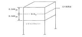
前記工程において、シリコン基板上にマスク物質を蒸着する段階は、シリコン基板の厚さと所望のナノギャップの大きさ(幅)から算出されるマスクパターンの大きさ(幅)に基づいてシリコン基板上にマスク物質を蒸着する段階から構成できる。すなわち、特定の厚さ(z)を持つシリコン基板があるとき、所望のナノギャップの大きさ、すなわち幅(wo)が定められると、下記数式1によって、シリコン基板上に蒸着されるマスク物質パターンの幅(wm)が決定される。この際、エッチング角度θはシリコン基板に応じて所定の値に予め定められる。
In the above process, the step of depositing the mask material on the silicon substrate is performed on the silicon substrate based on the mask pattern size (width) calculated from the thickness of the silicon substrate and the desired nanogap size (width). The method may comprise a step of depositing a mask material. That is, when there is a silicon substrate having a specific thickness (z) and a desired nanogap size, ie, width (w o ) is determined, a mask material deposited on the silicon substrate according to
![]()
![]()
前記数式1によって、シリコン基板の厚さ(z)およびマスク物質のパターン幅(wm)を調整することにより、本発明で製造されるシリコン基板上のナノギャップの幅(wo)を容易に調整することができる。
By adjusting the thickness (z) of the silicon substrate and the pattern width (w m ) of the mask material according to
シリコン基板上に蒸着されるマスク物質としては、上述したシリコン基板に対して異方性エッチングを行うために使用するKOH、TMAH、EDPなどのエッチング液によりエッチングされない物質を使用することが好ましく、特に好ましくはシリコン窒化膜(Si3N4)を使用することができる。ところが、マスク物質は、これに限定されず、SiO2など、当該分野における公知の任意のマスク物質を使用することができるのは勿論である。 As the mask material deposited on the silicon substrate, it is preferable to use a material that is not etched by an etchant such as KOH, TMAH, EDP, etc. used for performing anisotropic etching on the silicon substrate described above. Preferably, a silicon nitride film (Si 3 N 4 ) can be used. However, the mask material is not limited to this, and any mask material known in the art such as SiO 2 can be used.
マスク物質の上部に塗布されたフォトレジストを現像する段階は、当該分野で広く知られているように、好ましくは紫外線露光によって行われ得る。その後、マスク物質を除去する段階は、当該分野で広く知られているような活性イオンエッチング(RIE:Reactive Ion Etching)などの方法によって行われ、エッチングされるべき部分を露出させる。その後、レジストストリップ過程によって残余フォトレジストを除去することができる。レジストストリップ過程は、当該分野で通常用いられるように、アセトンに浸してフォトレジストを除去した後、メタノールで洗浄し、その後蒸留水で洗浄する工程で行われる。 The step of developing the photoresist applied on top of the mask material can be preferably performed by UV exposure, as is well known in the art. Thereafter, the mask material is removed by a method such as reactive ion etching (RIE), which is widely known in the art, to expose a portion to be etched. Thereafter, the remaining photoresist can be removed by a resist strip process. The resist strip process is performed in a process of immersing in acetone to remove the photoresist, washing with methanol, and then washing with distilled water, as is usually used in the art.
マスク物質の除去および残余フォトレジストの除去の後、好ましくは異方性エッチングが可能なエッチング液を用いてシリコン基板に対して断面V字形の形状に異方性エッチングを行うことにより、本発明に係るナノギャップを形成することができる。この際、好ましくは、前述したように異方性エッチングが可能なエッチング液によってシリコン基板をエッチングすることができるが、本発明の方法は、必ずしもこれに制限されるものではない。すなわち、例えばO2、CF4などのガスを用いたドライエッチングなど、当該分野における公知の任意の方法によって基板を断面V字形の形状にエッチングすることにより、本発明に係るナノギャップを製造することができるのは、当該分野における通常の知識を有する技術者には自明なことである。よって、それらの変更および修正は本発明の範囲に含まれる。この際、使用される基板もこれに制限されないが、前述したように異方性エッチングが行われる<100>タイプのシリコン基板が好ましい。 After removing the mask material and the remaining photoresist, the silicon substrate is preferably anisotropically etched into a V-shaped cross section using an etchant capable of anisotropic etching. Such a nanogap can be formed. At this time, the silicon substrate can be preferably etched with an etchant capable of anisotropic etching as described above, but the method of the present invention is not necessarily limited thereto. That is, the nanogap according to the present invention is manufactured by etching the substrate into a V-shaped cross section by any method known in the art, such as dry etching using a gas such as O 2 or CF 4. What can be done is obvious to engineers with ordinary knowledge in the field. Therefore, those changes and modifications are included in the scope of the present invention. At this time, the substrate to be used is not limited to this, but a <100> type silicon substrate on which anisotropic etching is performed as described above is preferable.
前述したような工程によってシリコン基板上にナノギャップを形成した後、本発明に係るナノギャップ製造方法は、好ましくはシリコン基板上の残余マスク物質を除去する段階をさらに含むことができる。シリコン基板上の残余マスク物質を除去する段階は、好ましくはHFなどを用いたウェットエッチングによって行われ得るが、必ずしもこれに限定されるものではなく、公知の任意の方法を用いてウェットまたはドライエッチングして除去することもできる。一方、使用されたシリコン基板がSOI(silicon on insulator)ウエハーの場合、ナノギャップ形成後の残余マスク物質の除去などと共に、ウェット或いはドライエッチングによって埋め込みシリコン酸化物(buried silicon oxide:SiO2)を除去する工程をさらに含むことが好ましい。この際、HFなどを用いたウェットエッチングによって残余マスク物質と埋め込み物質を同時に除去することもできる。 After forming the nanogap on the silicon substrate by the process as described above, the nanogap manufacturing method according to the present invention may further include removing a residual mask material on the silicon substrate. The step of removing the residual mask material on the silicon substrate may be performed by wet etching using HF or the like, but is not necessarily limited thereto, and wet or dry etching using any known method. It can also be removed. On the other hand, when the silicon substrate used is an SOI (silicon on insulator) wafer, the residual mask material after the nanogap formation is removed, and the buried silicon oxide (SiO 2 ) is removed by wet or dry etching. Preferably, the method further includes the step of: At this time, the residual mask material and the embedded material can be simultaneously removed by wet etching using HF or the like.
また、特に好ましい様態によれば、本発明に係るナノギャップ製造方法は、ナノギャップの大きさ(幅)をさらに減らすための工程として、シリコン基板上の残余マスク物質を除去する段階の後に酸化工程を行う段階をさらに含むことができる。本明細書に添付された図5から分かるように、前記工程によって製造されたナノギャップは、酸化工程によってその幅がさらに減少できることを確認することができる。酸化工程を行うと、図4に示すように、シリコン基板上に二酸化珪素(SiO2)が形成されてナノギャップの幅が減少するという効果が生ずる。酸化工程は、高温、例えば約1000℃の炉内におけるドライ酸化工程によって行われてもよく、短時間内に二酸化珪素を多量形成してナノギャップの間を減らすウェット酸化工程(wet oxidation)によって行われてもよい。ウェット酸化工程はドライ酸化工程より時間が少なくかかり、ドライ酸化工程はウェット工程より良い密度を示す。ドライ酸化工程は、酸素ガスの注入によって珪素原子(Si)と酸素(O2)との反応によって二酸化珪素(SiO2)を形成するが、これに対し、ウェット酸化工程は、水蒸気を用いることにより、珪素原子(Si)と水分子(H2O)とが反応して二酸化珪素(SiO2)と水素ガス(H2)を形成する。 According to a particularly preferable aspect, the nanogap manufacturing method according to the present invention includes an oxidation process after the step of removing the residual mask material on the silicon substrate as a process for further reducing the size (width) of the nanogap. The method may further include performing. As can be seen from FIG. 5 attached to the present specification, it can be confirmed that the nanogap produced by the above process can be further reduced in width by the oxidation process. When the oxidation process is performed, as shown in FIG. 4, silicon dioxide (SiO 2 ) is formed on the silicon substrate, and the nanogap width is reduced. The oxidation step may be performed by a dry oxidation step in a furnace at a high temperature, for example, about 1000 ° C. It may be broken. The wet oxidation process takes less time than the dry oxidation process, and the dry oxidation process exhibits a better density than the wet process. In the dry oxidation process, silicon dioxide (SiO 2 ) is formed by reaction of silicon atoms (Si) and oxygen (O 2 ) by oxygen gas injection, whereas in the wet oxidation process, water vapor is used. Then, silicon atoms (Si) and water molecules (H 2 O) react to form silicon dioxide (SiO 2 ) and hydrogen gas (H 2 ).
本発明は、別の様態として、前記本発明の方法によって製造されたナノギャップを用いたナノギャップセンサの製造方法を提供する。具体的に、前記ナノギャップセンサの製造方法は、前記方法によって製造されたナノギャップが形成された基板上に絶縁物質を蒸着する段階と、ナノギャップ電極を形成する段階とを含んでなる。 As another aspect, the present invention provides a method for producing a nanogap sensor using the nanogap produced by the method of the present invention. Specifically, the method of manufacturing the nanogap sensor includes a step of depositing an insulating material on a substrate having the nanogap manufactured by the method and a step of forming a nanogap electrode.
前述したように、本発明に係るナノギャップは、その間にナノメートル水準の大きさを持つ分子や細胞、抗原−抗体などの生物学的試料を位置させることにより、それらの分子的特性または存在有無などを検出するためのバイオセンサとして用いられることが求められる。このため、ナノギャップセンサの提供は、ナノギャップ上に、センサの役割を果たす電極を形成する工程、および付加的にパッシベーション工程を行うことにより達成できる。 As described above, the nanogap according to the present invention is a molecule, cell, or biological sample such as an antigen-antibody having a size of nanometer level between them. It is required to be used as a biosensor for detecting the above. For this reason, provision of a nanogap sensor can be achieved by forming an electrode serving as a sensor on the nanogap, and additionally performing a passivation step.
ナノギャップ上に電極を形成する方法は、電極として用いられる金属の蒸着とフォト作業によって電極を形成することができる。この際、フォト作業はフォトレジストを塗布し、マスクパターンに応じて紫外線露光を行って現像した後、金属エッチング液によって、電極を形成した金属を除去し、その後フォトレジストを除去する段階で行われる。電極を形成する金属物質としては、伝導性がある限りは特に制限されないが、金、銀、クロム、チタン、白金、銅、アルミニウム、パラジウム、ITOまたはこれらの合金が好ましい。金属蒸着工程は、平均自由行路(mean free path)の長い電子ビーム蒸着方法を採用することが好ましい。 In the method of forming an electrode on the nanogap, the electrode can be formed by vapor deposition of a metal used as the electrode and a photo work. At this time, the photo work is performed at a stage where a photoresist is applied, UV exposure is performed according to the mask pattern, development is performed, the metal on which the electrode is formed is removed with a metal etching solution, and then the photoresist is removed. . The metal material forming the electrode is not particularly limited as long as it has conductivity, but gold, silver, chromium, titanium, platinum, copper, aluminum, palladium, ITO, or an alloy thereof is preferable. The metal deposition process preferably employs an electron beam deposition method having a long mean free path.
金属蒸着の後、ナノギャップセンサのセンサ役割を果たす部分を除いた残部に対してAl2O3、SiO2などの物質を用いてパッシベーション工程をさらに行うことができるが、パッシベーションは、反応させる物質がナノギャップセンサのセンサ以外の部分には付着しないようにすることにより、ナノギャップセンサを用いた測定の際により少ない試料が消費されるようにすることができる。パッシベーション工程も、平均自由行路の長い電子ビーム蒸着方法を用いて行うことができる。パッシベーション物質としては、前述した物質の他にも、絶縁物質であって電子ビーム蒸着が可能な他の物質も使用することができる。 After metal deposition, a passivation process can be further performed using a material such as Al 2 O 3 , SiO 2 on the remainder excluding the portion that functions as a sensor of the nanogap sensor. By preventing from adhering to the part other than the sensor of the nanogap sensor, it is possible to consume a smaller amount of sample in the measurement using the nanogap sensor. The passivation process can also be performed using an electron beam evaporation method with a long mean free path. As the passivation material, in addition to the materials described above, other materials which are insulating materials and can be subjected to electron beam evaporation can be used.
本発明の別の様態では、前記のように製造されたナノギャップセンサを提供する。 In another aspect of the present invention, a nanogap sensor manufactured as described above is provided.
前記のように製造された本発明に係るナノギャップセンサは、電圧−電流特性を備え、電気的、化学的、電気化学的、生物学的分析対象物の濃度によって電流が変わるか、或いはナノメートルサイズ水準の分析対象物と特異的結合体との間に生ずる結合イベントが前記センサの電圧−電流特性で検出可能な変化を起こすことを感知することができることを特徴とする、ナノギャップセンサである。 The nanogap sensor according to the present invention manufactured as described above has voltage-current characteristics, and the current varies depending on the concentration of an electrical, chemical, electrochemical, or biological analyte, or is nanometer. A nanogap sensor characterized in that it can sense that a binding event occurring between a size level analyte and a specific conjugate causes a detectable change in the voltage-current characteristics of the sensor. .
前述したナノメートルサイズ水準の分析対象物とは、好ましくは細胞、DNA、タンパク質、抗原−抗体、酵素−基質などを意味する。したがって、本発明に係るナノギャップセンサは、好ましくはバイオセンサとして使用できる。この際、分析する対象に応じて、前記ナノギャップセンサは様々に変形可能であるが、例えばDNA分子を分析する場合には、両末端がチオール基で終わるDNAを電極に固定し、その上に、分析するDNAなどを付着させることが可能な金粒子などを固定して使用することができ、タンパク質分析の際には電極をガラス、高分子またはセラミックなどで塗布し、露出した電極部分にシステインなどの適切なリンカーを付けることにより、ここに分析するタンパク質が付着するようにすることもできる。また、抗体−抗原反応を分析しようとする場合には、前述したようなリンカーに特定の抗体を結合させた後、ここに特異的な抗原が結合するようにすることもできる。このように本発明に係るナノギャップセンサは、分析物に応じて、当業者に自明な様々な形態の修正または変形を含むように考慮できる。それらの変更および修正は全て本発明の範囲に属する。 The aforementioned nanometer-size analytes preferably mean cells, DNA, proteins, antigen-antibodies, enzyme-substrates, and the like. Therefore, the nanogap sensor according to the present invention can be preferably used as a biosensor. At this time, the nanogap sensor can be variously modified according to the object to be analyzed. For example, when analyzing a DNA molecule, DNA having both ends terminated with a thiol group is fixed to an electrode, Gold particles that can be attached to the DNA to be analyzed can be fixed and used for protein analysis, and the electrode is coated with glass, polymer or ceramic for protein analysis, and cysteine is applied to the exposed electrode part. The protein to be analyzed can be attached here by attaching an appropriate linker such as. In addition, when analyzing an antibody-antigen reaction, a specific antibody can be bound to a linker as described above, and then a specific antigen can be bound thereto. Thus, the nanogap sensor according to the present invention can be considered to include various forms of modifications or variations obvious to those skilled in the art depending on the analyte. All such changes and modifications are within the scope of the present invention.
一方、本発明に係るナノギャップセンサの場合、前述したように、ナノギャップに形成された電極の表面にリンカーを介してまたはリンカーなしで直ちに電極の表面に抗体などの分析物を付着させることができることを特徴とする(図12)。これに反し、既存のナノギャップセンサでは、ナノギャップセンサを構成する電極の間の底部に分析対象物を付着させて測定する方法を使用する(図11)。本発明に係るナノギャップセンサにおいても、電極の間の底部に分析物を付着させて測定することもできるが、前述したように、電極に直接分析物を付着させることにより、測定する分子をより簡便に固定することができ、分析に必要な試料の量も既存のナノギャップセンサに比べて少量消費される。したがって、このようにナノギャップの電極上に直接分析物を付着させることができるように構成された本発明に係るナノギャップセンサが既存のナノギャップセンサに比べてより有用である。 On the other hand, in the case of the nanogap sensor according to the present invention, as described above, an analyte such as an antibody can be immediately attached to the surface of the electrode formed in the nanogap via a linker or without a linker. It is possible to perform (FIG. 12). On the other hand, the existing nanogap sensor uses a method in which an analyte is attached to the bottom between the electrodes constituting the nanogap sensor for measurement (FIG. 11). In the nanogap sensor according to the present invention, it is also possible to perform measurement by attaching an analyte to the bottom between the electrodes, but as described above, by attaching the analyte directly to the electrode, more molecules to be measured can be obtained. It can be easily fixed, and the amount of sample required for analysis is also consumed in a small amount compared to the existing nanogap sensor. Therefore, the nanogap sensor according to the present invention configured to attach the analyte directly on the nanogap electrode is more useful than the existing nanogap sensor.
本発明の別の様態では、前述したように製造された本発明に係るナノギャップセンサを用いて、ナノメートルサイズ水準の物質、例えば生物学的試料などの特性および電気、化学的性質などを分析する方法を提供する。 In another aspect of the present invention, the nanogap sensor according to the present invention manufactured as described above is used to analyze the properties of nanometer-sized substances, such as biological samples, and the electrical and chemical properties. Provide a way to do it.
上述した本発明に係るナノギャップおよびナノギャップセンサの製造方法によれば、半導体製造工程技術を用いて、高価の装備を使用することなく簡単且つ容易にナノギャップおよびナノギャップセンサを量産することができ、これにより多様な電極の生成、多様な物質の電気的特性の測定および多様なセンサへの応用が可能になった。 According to the above-described nanogap and nanogap sensor manufacturing method according to the present invention, it is possible to easily and easily mass-produce nanogap and nanogap sensors using semiconductor manufacturing process technology without using expensive equipment. This made it possible to create various electrodes, measure the electrical properties of various substances and apply them to various sensors.
以下に添付図面を参照しながら、本発明の一実施例に係る、シリコン基板を用いたナノギャップセンサの製作方法について詳細に説明する。 Hereinafter, a method of manufacturing a nanogap sensor using a silicon substrate according to an embodiment of the present invention will be described in detail with reference to the accompanying drawings.
図1は本発明の一実施例に係るナノギャップ製作方法の動作過程を示す概略順序図、図2は本発明の方法によってナノギャップを製造するためのシリコンの厚さとマスクパターンのサイズに対するギャップサイズの設定を数学的に説明するための図、図3は本発明の一実施例によってナノギャップセンサ製作方法の各工程を示す概略断面図、図4はシリコン酸化工程による二酸化珪素(SiO2)の形成を説明するための図、図5は酸化工程の後にギャップの大きさが減少した様子を示す図である。 FIG. 1 is a schematic flow chart showing an operation process of a nanogap fabrication method according to an embodiment of the present invention, and FIG. FIG. 3 is a schematic cross-sectional view showing each process of a nanogap sensor manufacturing method according to an embodiment of the present invention, and FIG. 4 is a diagram of silicon dioxide (SiO 2 ) formed by a silicon oxidation process. FIG. 5 is a diagram for explaining the formation, and FIG. 5 is a diagram showing a state in which the size of the gap is reduced after the oxidation process.
まず、図2に示すように、シリコン基板10の厚さと所望のナノギャップの大きさから算出されるマスクパターンの大きさに基づいてシリコン基板10上にマスク物質20を蒸着する(S10)(図3のa参照)。シリコン基板の厚さは、ナノギャップセンサにおいて基板上に金属を蒸着し得る程度の強度を持つことができれば、特に制限されない。上述したように、好ましくは、シリコン基板10は異方性エッチングが可能な<100>タイプを使用する。
First, as shown in FIG. 2, a mask material 20 is deposited on the
前述したように、シリコン基板10上に蒸着されるマスク物質20は、異方性エッチングのためのKOH、TMAH、EDPなどのエッチング液によってエッチングされないシリコン窒化膜(Si3N4)またはSiO2などを使用することが好ましい。
As described above, the mask material 20 deposited on the
上述した段階(S10)によってシリコン基板10上にマスク物質20を蒸着した後、蒸着されたマスク物質20の上部にフォトレジスト30を塗布する(S20)(図3のb参照)。マスク物質20の上部にフォトレジスト30を塗布した後には、紫外線(UV)露光を行い、マスク物質20の上部に塗布されたフォトレジストを現像する(S30)(図3のc参照)。そして、活性イオンエッチング(RIE:Reactive Ion Etching)を介してマスク物質20を除去して、エッチングされる部分を露出させ、残余フォトレジスト30を除去する(S40)(図3のd参照)。
After the mask material 20 is deposited on the
その後、エッチング液を用いてシリコン基板10に対して断面V字形の形状に異方性エッチングを行ってナノギャップを形成する(S50)(図3のe参照)。この際、シリコン基板10の厚さをエッチング率(etch rate)で割ると、必要なエッチング時間を計算することができる。
Thereafter, anisotropic etching is performed on the
異方性エッチングによってナノギャップを形成した後には、シリコン基板10上の残余マスク物質20と埋め込まれた二酸化珪素40を除去する(S60)(図3のf参照)。この際、残余マスク物質20と埋め込まれた二酸化珪素40を除去する方法として、HFウェットエッチングを行うことが最も好ましいが、これに限定されない。
After the nanogap is formed by anisotropic etching, the residual mask material 20 and the embedded silicon dioxide 40 on the
次に、ナノギャップの大きさを減らすための酸化工程を行う(S70)。図5は酸化工程によってナノギャップの大きさが減少することを説明した図である。酸化工程を行うと、図4に示すように、シリコン基板上に二酸化珪素(SiO2)が形成されるが、二酸化珪素を短時間内に多量形成してナノギャップの大きさを速く減らすためには、ウェット酸化工程(wet oxidation)を行うことが好ましい。 Next, an oxidation process is performed to reduce the size of the nanogap (S70). FIG. 5 is a diagram illustrating that the size of the nanogap is reduced by the oxidation process. When the oxidation process is performed, as shown in FIG. 4, silicon dioxide (SiO 2 ) is formed on the silicon substrate. In order to quickly reduce the size of the nanogap by forming a large amount of silicon dioxide in a short time. It is preferable to perform a wet oxidation process.
ナノギャップを形成した後、センサの役割を果たす電極を形成し、その後パッシベーション工程を行う。電極の形成は、フォト作業によって、電極として用いる金属を、ナノギャップを形成する両側壁上に蒸着させることにより行われる。金属蒸着過程において、平均自由行路の長い電子ビーム蒸着方法を用いることが好ましく、金属蒸着の後、パッシベーション過程においても、パッシベーションすべき物質を平均自由行路の長い電子ビーム蒸着方法を用いて蒸着させることが好ましい。電極を形成する金属物質は、伝導性がある限りは特に制限されないが、好ましくは金、白金、銅、またはこれらの合金である。 After forming the nanogap, an electrode serving as a sensor is formed, and then a passivation process is performed. Formation of an electrode is performed by vapor-depositing the metal used as an electrode on both side walls which form a nano gap by a photo work. In the metal vapor deposition process, it is preferable to use an electron beam vapor deposition method with a long mean free path. After the metal vapor deposition, the material to be passivated is vapor deposited using an electron beam vapor deposition method with a long mean free path. Is preferred. The metal material forming the electrode is not particularly limited as long as it has conductivity, but is preferably gold, platinum, copper, or an alloy thereof.
以下、本発明を好適な実施例を挙げて詳細に説明したが、本発明は、下記実施例に限定されるものではなく、当該分野における通常の知識を有する者であれば、本発明の技術的思想の範囲内において各種変形が可能なのは明らかである。 Hereinafter, the present invention has been described in detail with reference to preferred examples. However, the present invention is not limited to the following examples, and those skilled in the art will be able to use the technology of the present invention. It is clear that various modifications are possible within the scope of the ideal idea.
〔実施例1:ナノギャップの製作〕
厚さ500μmの4インチ<100>シリコン基板を準備し、エッチング液としてKOHを準備した。この際、図2におけるθ値は約54.6°(理論的には54.74°)である。このようにθ値とシリコン基板の厚さが定められることにより、図2に示した数式によって幅が714μmと決定された長方形の形状を持つフォトマスクを準備した。
[Example 1: Production of nanogap]
A 4-inch <100> silicon substrate having a thickness of 500 μm was prepared, and KOH was prepared as an etching solution. At this time, the θ value in FIG. 2 is about 54.6 ° (theoretically 54.74 °). Thus, by defining the θ value and the thickness of the silicon substrate, a photomask having a rectangular shape whose width was determined to be 714 μm by the mathematical formula shown in FIG. 2 was prepared.
準備されたシリコン基板上に、エッチング液としてのKOHによりほぼエッチングされないSi3N4をLPCVD(Low Pressure Chemical Vapor Deposition)を用いて200nmの厚さに蒸着し、その後蒸着されたSi3N4の上部にフォトレジストAZ5214E(米国、Clariant社製)を2μmの厚さに塗布した後、紫外線露光を行い、Si3N4の上部に塗布されたフォトレジストを現像した。
その後、長方形のパターン部分のフォトレジストを除去し、活性イオンエッチングによってSi3N4を除去することにより、KOHによってエッチングが行われる部分を露出させた。
On the prepared silicon substrate, Si 3 N 4 that is hardly etched by KOH as an etching solution is deposited to a thickness of 200 nm using LPCVD (Low Pressure Chemical Vapor Deposition), and then the deposited Si 3 N 4 is deposited. Photoresist AZ5214E (manufactured by Clariant, USA) was applied to a thickness of 2 μm on the top, and then exposed to ultraviolet light to develop the photoresist applied on top of Si 3 N 4 .
Thereafter, the photoresist in the rectangular pattern portion was removed, and Si 3 N 4 was removed by active ion etching, thereby exposing the portion to be etched with KOH.
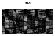
次いで、残余フォトレジストの除去およびクリーニングを行った後、均一且つ高いエッチング率を得るために20%のKOHを用いて80℃で約6時間異方性エッチングを行うことにより、ナノギャップを形成した。この際のエッチング率は約1.4μm/min程度である。図7の電子顕微鏡写真は、このようにKOHを用いて異方性エッチングを行った後、生成されたナノギャップの模様を示す。
その次、異方性エッチングにより生成されたナノギャップの大きさをさらに減らすために、シリコン基板上の残余Si3N4を、49%のHFを用いたウェットエッチングによって除去し、綺麗にクリーニング処理した後、1000℃の炉(furnace)でドライ酸化工程を行った。図8の電子顕微鏡写真は、このような酸化工程によってナノギャップの大きさがさらに減少したことを示す。
Next, after removing and cleaning the remaining photoresist, a nanogap was formed by performing anisotropic etching at 80 ° C. for about 6 hours using 20% KOH in order to obtain a uniform and high etching rate. . The etching rate at this time is about 1.4 μm / min. The electron micrograph of FIG. 7 shows the pattern of the nanogap generated after anisotropic etching using KOH in this way.
Next, in order to further reduce the size of the nanogap generated by anisotropic etching, the remaining Si 3 N 4 on the silicon substrate is removed by wet etching using 49% HF, and cleanly processed. Then, a dry oxidation process was performed in a 1000 ° C. furnace. The electron micrograph of FIG. 8 shows that the size of the nanogap was further reduced by such an oxidation process.
〔実施例2:ナノギャップセンサの製作〕
トップシリコンが1μmの厚さを有し、375nmの埋め込み二酸化珪素(buried silicon dioxide)を持つ4インチ<100>シリコン基板を準備し、エッチング液としてKOHを準備した。図2におけるθ値が約54.6°(理論的に54.74°)と設定されることにより、図2に示した数式によって幅が1.4μmと決定された長方形のフォトマスクを準備した。
[Example 2: Production of nanogap sensor]
A 4 inch <100> silicon substrate with a top silicon thickness of 1 μm and 375 nm buried silicon dioxide was prepared and KOH was prepared as an etchant. By setting the θ value in FIG. 2 to about 54.6 ° (theoretically 54.74 °), a rectangular photomask whose width was determined to be 1.4 μm by the formula shown in FIG. 2 was prepared. .
準備されたシリコン基板上に、エッチング液としてのKOHによりほぼエッチングされないSi3N4をLPCVD(Low Pressure Chemical Vapor Deposition)を用いて200nmの厚さに蒸着し、蒸着されたSi3N4の上部にフォトレジストAZ5214E(米国、Clariant社製)を2μmの厚さに塗布した後、紫外線露光を行い、Si3N4の上部に塗布されたフォトレジストを現像した。その後、長方形からなるパターン部分のフォトレジストを除去し、活性イオンエッチングによってSi3N4を除去することにより、KOHによりエッチングが行われる部分を露出させた。 On the prepared silicon substrate, Si 3 N 4 that is hardly etched by KOH as an etchant is deposited to a thickness of 200 nm using LPCVD (Low Pressure Chemical Vapor Deposition), and the upper part of the deposited Si 3 N 4 A photoresist AZ5214E (manufactured by Clariant, USA) was applied to a thickness of 2 μm, and then exposed to ultraviolet light to develop the photoresist applied on top of Si 3 N 4 . Thereafter, the photoresist of the rectangular pattern portion was removed, and Si 3 N 4 was removed by active ion etching, thereby exposing the portion to be etched with KOH.
次いで、残余フォトレジストの除去およびクリーニングを行った後、均一且つ高いエッチング率を得るために20%のKOHを用いて80℃で約60〜90秒間異方性エッチングを行うことにより、ナノギャップを形成した。この際、エッチング率は約1.4μm/min程度である。 Next, after removing the remaining photoresist and cleaning, anisotropic etching is performed at 80 ° C. for about 60 to 90 seconds using 20% KOH in order to obtain a uniform and high etching rate. Formed. At this time, the etching rate is about 1.4 μm / min.
その次、異方性エッチングにより生成されたナノギャップの大きさをさらに減らすために、シリコン基板上の残余Si3N4を49%のHFを用いてウェットエッチングによって除去し、綺麗にクリーニング処理した後、1000℃の炉でドライ酸化工程を行った。
図6はこのようにKOHを用いて異方性エッチングを行った後、HFウェットエッチングを行うことにより生成されたナノギャップの電子顕微鏡写真である。
Next, in order to further reduce the size of the nanogap generated by anisotropic etching, the remaining Si 3 N 4 on the silicon substrate was removed by wet etching using 49% HF and cleaned cleanly. Thereafter, a dry oxidation process was performed in a 1000 ° C. furnace.
FIG. 6 is an electron micrograph of a nanogap generated by performing anisotropic etching using KOH and then performing HF wet etching.
次いで、電子ビーム蒸着器を用いて電極形成物質としてのCr/Auを蒸着し、フォト作業によって電極を形成した後、電子ビーム蒸着器を用いてAl2O3を蒸着してセンサ部分以外の残部をパッシベーションすることにより、ナノギャップセンサを製作した。 Next, Cr / Au as an electrode forming material is vapor-deposited using an electron beam vapor deposition device, an electrode is formed by a photo work, and then Al 2 O 3 is vapor deposited using an electron beam vapor deposition device, and the rest other than the sensor portion A nanogap sensor was fabricated by passivation.
〔実施例3:ナノギャップセンサを用いた生体物質の測定〕
実施例2で製作されたナノギャップセンサによって生体物質の測定を行う。前記ナノギャップセンサの露出した金電極部分に、抗体と安定的に結合可能なリンカーをまず付着させた後、ここに抗−PSA(prostate specific antigen)抗体を結合させた。この際、使用したリンカーは、本発明者等によって韓国特許出願第2006−57140号に開示されたような、N末端に3つのシステインがタグれたタンパク質Gリンカーを使用した。固体支持体に抗体を安定的に結合させるためにタンパク質Gを変形して使用した例があったが、前記韓国特許出願第2006−57140号に開示されたタンパク質Gリンカーの場合、N末端に1〜5個のシステインをタグすることにより、より安定的に抗体を固定することができることを見出し、特にシステインを1〜3個結合させたタンパク質Gがより安定的に抗体を固定することをできることを見出した。この際、タンパク質Gはタンパク質G全体を使用することもできるが、抗体結合部位であるB1およびB2領域のみを取って、そのN末端に1〜5個のシステインをタグしたものと同一の効果を示すことを確認した。したがって、本発明では、タンパク質GのB1およびB2領域のN末端にシステインがタグされたリンカーを使用した。前記リンカーのN末端システインは、金との親和度を持つことにより、本発明に係るナノギャップセンサの金電極上によく吸着した。本実施例では、このようなリンカーが付いたナノギャップセンサ上に抗−PSA抗体を固定した後、ここに10ng/mL、1ng/mLおよび100pg/mLの濃度でPSAを適用させてナノギャップセンサの電流を測定した。
[Example 3: Measurement of biological material using a nanogap sensor]
The biological material is measured by the nanogap sensor manufactured in Example 2. A linker capable of stably binding to an antibody was first attached to the exposed gold electrode portion of the nanogap sensor, and then an anti-PSA (prostate specific antigen) antibody was bound thereto. At this time, the linker used was a protein G linker tagged with three cysteines at the N-terminus as disclosed in Korean Patent Application No. 2006-57140 by the present inventors. There has been an example in which protein G is modified and used to stably bind an antibody to a solid support. It is found that by tagging ˜5 cysteines, the antibody can be more stably immobilized, and in particular, protein G to which 1 to 3 cysteines are bound can immobilize the antibody more stably. I found it. At this time, the whole protein G can be used as the protein G, but only the B1 and B2 regions which are antibody binding sites are taken and the same effect as that obtained by tagging 1 to 5 cysteines at the N-terminus thereof is obtained. Confirmed to show. Therefore, in the present invention, a linker having a cysteine tag at the N-terminus of the B1 and B2 regions of protein G was used. The N-terminal cysteine of the linker was well adsorbed on the gold electrode of the nanogap sensor according to the present invention by having an affinity for gold. In this example, an anti-PSA antibody was immobilized on a nanogap sensor with such a linker, and then PSA was applied thereto at concentrations of 10 ng / mL, 1 ng / mL, and 100 pg / mL to thereby form a nanogap sensor. Current was measured.
図9はこのような方法によって製作された本発明に係るナノギャップセンサ上に抗体および抗原が適用された様子を概略的に示す。図10は前記方法によって製作されたナノギャップセンサによって前記PSAの濃度による電流の変化を測定して示すグラフである。 FIG. 9 schematically shows that an antibody and an antigen are applied to the nanogap sensor according to the present invention manufactured by such a method. FIG. 10 is a graph showing a change in current due to the concentration of the PSA measured by the nanogap sensor manufactured by the above method.
以上、本発明を好適な実施例によって説明したが、これは例示のためのものに過ぎず、当該技術分野における熟練した技術者であれば、下記特許請求の範囲に記載された本願発明の思想および領域から逸脱しない範囲内において、本発明に様々な修正および変更を加え得ることが理解できるであろう。 Although the present invention has been described by way of a preferred embodiment, this is merely for the purpose of illustration, and a person skilled in the art can think of the present invention described in the following claims. It will be understood that various modifications and changes may be made to the present invention without departing from the scope and scope.
10 シリコン基板
20 マスク物質
30 フォトレジスト
40 埋め込み二酸化珪素
50 電極物質
60 パッシベーション物質
10 Silicon Substrate 20 Mask Material 30 Photoresist 40 Embedded Silicon Dioxide 50 Electrode Material 60 Passivation Material
Claims (42)
a)前記基板上にマスク物質を蒸着する段階と、
b)蒸着された前記マスク物質の上部にフォトレジストを塗布する段階と、
c)塗布された前記フォトレジストを現象する段階と、
d)前記マスク物質を除去して、エッチングされる部分を露出させる段階とを含む、請求項1〜10のいずれか一つに記載の方法。 Before etching the substrate,
a) depositing a mask material on the substrate;
b) applying a photoresist on top of the deposited mask material;
c) phenomenon of the applied photoresist;
and d) removing the mask material to expose a portion to be etched.
The nanogap sensor according to any one of claims 39 to 41, wherein the electrode is made of gold.
Applications Claiming Priority (3)
| Application Number | Priority Date | Filing Date | Title |
|---|---|---|---|
| KR20050099585 | 2005-10-21 | ||
| KR1020060072981A KR100849384B1 (en) | 2005-10-21 | 2006-08-02 | A method for fabricating nanogap and nanogap sensor |
| PCT/KR2006/003517 WO2007046582A1 (en) | 2005-10-21 | 2006-09-05 | A method for fabricating nanogap and nanogap sensor |
Publications (2)
| Publication Number | Publication Date |
|---|---|
| JP2009521332A true JP2009521332A (en) | 2009-06-04 |
| JP2009521332A5 JP2009521332A5 (en) | 2009-07-23 |
Family
ID=38178037
Family Applications (1)
| Application Number | Title | Priority Date | Filing Date |
|---|---|---|---|
| JP2008536478A Pending JP2009521332A (en) | 2005-10-21 | 2006-09-05 | Manufacturing method of nanogap and nanogap sensor |
Country Status (4)
| Country | Link |
|---|---|
| US (1) | US8557567B2 (en) |
| JP (1) | JP2009521332A (en) |
| KR (1) | KR100849384B1 (en) |
| CN (1) | CN101156228B (en) |
Cited By (2)
| Publication number | Priority date | Publication date | Assignee | Title |
|---|---|---|---|---|
| WO2011081245A1 (en) * | 2009-12-29 | 2011-07-07 | 연세대학교 산학협력단 | Hydrogen sensor, and method for fabricating same |
| JP2022500628A (en) * | 2018-09-14 | 2022-01-04 | アプライド マテリアルズ インコーポレイテッドApplied Materials, Incorporated | How to form nanopores and the resulting structure |
Families Citing this family (25)
| Publication number | Priority date | Publication date | Assignee | Title |
|---|---|---|---|---|
| KR101518733B1 (en) | 2008-11-27 | 2015-05-11 | 삼성전자주식회사 | Nozzle plate and method of manufacturing the same |
| US20110020966A1 (en) * | 2009-07-23 | 2011-01-27 | Canon Kabushiki Kaisha | Method for processing silicon substrate and method for producing substrate for liquid ejecting head |
| KR101130084B1 (en) * | 2010-04-28 | 2012-03-28 | 연세대학교 산학협력단 | hydrogen sensor and manufacturing method thereof |
| JP5145463B2 (en) * | 2009-12-29 | 2013-02-20 | インダストリー−アカデミック コーペレイション ファウンデイション, ヨンセイ ユニバーシティ | Hydrogen sensor and manufacturing method thereof |
| WO2011108540A1 (en) | 2010-03-03 | 2011-09-09 | 国立大学法人大阪大学 | Method and device for identifying nucleotide, and method and device for determining nucleotide sequence of polynucleotide |
| KR20110138657A (en) * | 2010-06-21 | 2011-12-28 | (주)미코바이오메드 | Surface plasmon resonance sensor module and sensing system having the same |
| KR101694549B1 (en) * | 2010-10-21 | 2017-01-09 | (주)미코바이오메드 | Method of forming a nano-gap pattern, bio sensor and method of manufacturing a bio sensor including a nano-gap pattern |
| CA2882001A1 (en) | 2012-08-17 | 2014-02-20 | Osaka University | Sample analysis method |
| KR101878747B1 (en) | 2012-11-05 | 2018-07-16 | 삼성전자주식회사 | Nanogap device and signal processing method from the same |
| KR101927415B1 (en) | 2012-11-05 | 2019-03-07 | 삼성전자주식회사 | Nanogap device and signal processing method from the same |
| JP6282036B2 (en) | 2012-12-27 | 2018-02-21 | クオンタムバイオシステムズ株式会社 | Method and control apparatus for controlling movement speed of substance |
| CN106104274B (en) | 2013-09-18 | 2018-05-22 | 量子生物有限公司 | biomolecule sequencing device, system and method |
| JP2015077652A (en) | 2013-10-16 | 2015-04-23 | クオンタムバイオシステムズ株式会社 | Nano-gap electrode and method for manufacturing same |
| US10438811B1 (en) | 2014-04-15 | 2019-10-08 | Quantum Biosystems Inc. | Methods for forming nano-gap electrodes for use in nanosensors |
| US9343569B2 (en) | 2014-05-21 | 2016-05-17 | International Business Machines Corporation | Vertical compound semiconductor field effect transistor on a group IV semiconductor substrate |
| CN106796196A (en) * | 2014-07-11 | 2017-05-31 | 牛津大学科技创新有限公司 | Method for forming nano gap in Graphene |
| DE102015211392B4 (en) | 2015-06-19 | 2018-05-24 | Albert-Ludwigs-Universität Freiburg | Electrode structure and method for producing the electrode structure and biosensor chip comprising the electrode structure |
| US10247700B2 (en) | 2015-10-30 | 2019-04-02 | International Business Machines Corporation | Embedded noble metal electrodes in microfluidics |
| CN115595360A (en) | 2016-04-27 | 2023-01-13 | 因美纳剑桥有限公司(Gb) | Systems and methods for measurement and sequencing of biomolecules |
| US11673136B2 (en) * | 2017-04-04 | 2023-06-13 | Arizona Board Of Regents On Behalf Of Arizona State University | Nanopore devices for sensing biomolecules |
| US11740226B2 (en) | 2017-10-13 | 2023-08-29 | Analog Devices International Unlimited Company | Designs and fabrication of nanogap sensors |
| WO2019217600A1 (en) | 2018-05-09 | 2019-11-14 | Stuart Lindsay | Method for electronic detection and quantification of antibodies |
| EP3793721A4 (en) | 2018-05-17 | 2022-07-20 | Recognition Analytix, Inc. | Device, system and method for direct electrical measurement of enzyme activity |
| EP4110951A4 (en) | 2020-02-28 | 2024-03-20 | Arizona Board of Regents on behalf of Arizona State University | Methods for sequencing biopolymers |
| KR20230060124A (en) * | 2021-10-27 | 2023-05-04 | 현대자동차주식회사 | Hydrogen sensor and hydrogen sensor manufacturing method |
Citations (1)
| Publication number | Priority date | Publication date | Assignee | Title |
|---|---|---|---|---|
| JP2005278916A (en) * | 2004-03-30 | 2005-10-13 | Sanyo Product Co Ltd | Game machine |
Family Cites Families (30)
| Publication number | Priority date | Publication date | Assignee | Title |
|---|---|---|---|---|
| US6207369B1 (en) * | 1995-03-10 | 2001-03-27 | Meso Scale Technologies, Llc | Multi-array, multi-specific electrochemiluminescence testing |
| WO1998035012A2 (en) * | 1997-02-12 | 1998-08-13 | Chan Eugene Y | Methods and products for analyzing polymers |
| JP3794461B2 (en) | 1999-04-30 | 2006-07-05 | 日本電信電話株式会社 | Electron crystal or hole crystal |
| JP2000315785A (en) * | 1999-04-30 | 2000-11-14 | Canon Inc | Manufacture of nano structural member and nano structural member device |
| EP2383776B1 (en) * | 1999-06-22 | 2015-02-25 | President and Fellows of Harvard College | Solid state nanopore device for evaluating biopolymers |
| US6897009B2 (en) | 1999-11-29 | 2005-05-24 | Trustees Of The University Of Pennsylvania | Fabrication of nanometer size gaps on an electrode |
| US8232582B2 (en) * | 2000-04-24 | 2012-07-31 | Life Technologies Corporation | Ultra-fast nucleic acid sequencing device and a method for making and using the same |
| US7001792B2 (en) | 2000-04-24 | 2006-02-21 | Eagle Research & Development, Llc | Ultra-fast nucleic acid sequencing device and a method for making and using the same |
| US7291284B2 (en) * | 2000-05-26 | 2007-11-06 | Northwestern University | Fabrication of sub-50 nm solid-state nanostructures based on nanolithography |
| US7148058B2 (en) * | 2000-06-05 | 2006-12-12 | Chiron Corporation | Protein microarrays on mirrored surfaces for performing proteomic analyses |
| KR20030052665A (en) * | 2001-12-21 | 2003-06-27 | 주식회사 하이닉스반도체 | Method for forming nano space pattern |
| DE10204690A1 (en) | 2002-02-06 | 2003-08-07 | Clariant Gmbh | Process for the preparation of synergistic stabilizer mixtures |
| US7005264B2 (en) * | 2002-05-20 | 2006-02-28 | Intel Corporation | Method and apparatus for nucleic acid sequencing and identification |
| EP1366860B1 (en) | 2002-05-28 | 2005-03-23 | Asia Pacific Microsystem, Inc. | Non-destructive method for measuring the thickness of a bonded wafer |
| WO2004077503A2 (en) | 2003-02-03 | 2004-09-10 | President And Fellows Of Harvard College | Controlled fabrication of gaps in electrically conducting structures |
| JP3787630B2 (en) * | 2003-02-14 | 2006-06-21 | 独立行政法人情報通信研究機構 | Manufacturing method of nanogap electrode |
| NL1022855C2 (en) | 2003-03-05 | 2004-09-07 | Univ Delft Tech | Method and device for the controlled manufacture of openings on a nanometer scale. |
| US7172917B2 (en) * | 2003-04-17 | 2007-02-06 | Robert Bosch Gmbh | Method of making a nanogap for variable capacitive elements, and device having a nanogap |
| JP3864229B2 (en) * | 2003-08-29 | 2006-12-27 | 独立行政法人産業技術総合研究所 | Method for producing nanogap electrode and device having nanogap electrode produced by the method |
| WO2005069001A1 (en) * | 2003-09-25 | 2005-07-28 | Toyama Prefecture | Microwell array chip and its manufacturing method |
| US7851203B2 (en) * | 2003-10-01 | 2010-12-14 | Lawrence Livermore National Security, Llc | Functionalized apertures for the detection of chemical and biological materials |
| KR100561908B1 (en) | 2003-12-26 | 2006-03-20 | 한국전자통신연구원 | Sensor Structure and Method thereof |
| WO2006137891A2 (en) * | 2004-09-29 | 2006-12-28 | University Of Florida Research Foundation, Inc. | Membrane with nanochannels for detection of molecules |
| US20060073489A1 (en) * | 2004-10-05 | 2006-04-06 | Gangqiang Li | Nanopore separation devices and methods of using same |
| KR100679704B1 (en) * | 2005-01-10 | 2007-02-06 | 한국과학기술원 | Manufacturing method of Nanogap or nanoFET for molecular device and bio-sensor |
| US7947485B2 (en) * | 2005-06-03 | 2011-05-24 | Hewlett-Packard Development Company, L.P. | Method and apparatus for molecular analysis using nanoelectronic circuits |
| US7410762B1 (en) * | 2005-06-27 | 2008-08-12 | Sandia Corporation | Method for detecting biomolecules |
| TW200700038A (en) * | 2005-06-27 | 2007-01-01 | Chieh Shang Co Ltd | Inflatable air cushion |
| US8860438B2 (en) * | 2009-05-11 | 2014-10-14 | Clemson University Research Foundation | Electrical double layer capacitive devices and methods of using same for sequencing polymers and detecting analytes |
| KR200457140Y1 (en) | 2010-01-22 | 2011-12-06 | (주)파트론정밀 | Flexible Flat Cable Connector |
-
2006
- 2006-08-02 KR KR1020060072981A patent/KR100849384B1/en active IP Right Grant
- 2006-09-05 JP JP2008536478A patent/JP2009521332A/en active Pending
- 2006-09-05 US US11/887,978 patent/US8557567B2/en active Active
- 2006-09-05 CN CN200680011497.0A patent/CN101156228B/en not_active Expired - Fee Related
Patent Citations (1)
| Publication number | Priority date | Publication date | Assignee | Title |
|---|---|---|---|---|
| JP2005278916A (en) * | 2004-03-30 | 2005-10-13 | Sanyo Product Co Ltd | Game machine |
Non-Patent Citations (1)
| Title |
|---|
| YANG-KYU CHOI: "Sublithographic nanofabrication technology for nanocatalystsand DNA chips", J. VAC. SCI. TECHNOL. B,, vol. Vol. 21, No. 6,, JPN6011058407, 2003, pages 2951 - 2955, ISSN: 0002063554 * |
Cited By (4)
| Publication number | Priority date | Publication date | Assignee | Title |
|---|---|---|---|---|
| WO2011081245A1 (en) * | 2009-12-29 | 2011-07-07 | 연세대학교 산학협력단 | Hydrogen sensor, and method for fabricating same |
| KR101067557B1 (en) | 2009-12-29 | 2011-09-27 | 연세대학교 산학협력단 | hydrogen sensor and manufacturing method thereof |
| JP2022500628A (en) * | 2018-09-14 | 2022-01-04 | アプライド マテリアルズ インコーポレイテッドApplied Materials, Incorporated | How to form nanopores and the resulting structure |
| JP7190558B2 (en) | 2018-09-14 | 2022-12-15 | アプライド マテリアルズ インコーポレイテッド | Methods of forming nanopores and resulting structures |
Also Published As
| Publication number | Publication date |
|---|---|
| US20090215156A1 (en) | 2009-08-27 |
| US8557567B2 (en) | 2013-10-15 |
| KR20070043591A (en) | 2007-04-25 |
| KR100849384B1 (en) | 2008-07-31 |
| CN101156228B (en) | 2013-01-30 |
| CN101156228A (en) | 2008-04-02 |
Similar Documents
| Publication | Publication Date | Title |
|---|---|---|
| JP2009521332A (en) | Manufacturing method of nanogap and nanogap sensor | |
| US7824620B2 (en) | Nano- and micro-scale structures: methods, devices and applications thereof | |
| US20200393440A1 (en) | Method, apparatus and system for single-molecule polymerase biosensor with transition metal nanobridge | |
| JP4213668B2 (en) | Molecular electronics and semiconductor device for biosensor device based on molecular electronics and manufacturing method thereof | |
| TWI424160B (en) | Sensing element integrating silicon nanowire gated-diodes, manufacturing method and detecting system thereof | |
| JP2012163578A (en) | Methods of using and constructing nanosensor platforms | |
| US8241939B2 (en) | Semiconductor nanowire sensor device and method for manufacturing the same | |
| KR101489154B1 (en) | Method for manufacturing nanogap sensor using residual stress and nanogap sensor manufactured thereby | |
| US20210396708A1 (en) | Methods for detecting analytes using a graphene-based biological field-effect transistor | |
| US20220091066A1 (en) | Biofunctionalized three-dimensional (3d) graphene-based field-effect transistor (fet) sensor | |
| Partel et al. | Lift-off free fabrication approach for periodic structures with tunable nano gaps for interdigitated electrode arrays | |
| US20160252506A1 (en) | Silicon nanowire-based sensor arrays | |
| Sinha et al. | Selective, ultra-sensitive, and rapid detection of serotonin by optimized ZnO nanorod FET biosensor | |
| Adam et al. | Recent advances in techniques for fabrication and characterization of nanogap biosensors: A review | |
| CN103922275B (en) | Self-formed Nanometer Channel At Wafer Scale And Method For Manufacturing Same | |
| WO2008021614A2 (en) | Coded particle arrays for high throughput analyte analysis | |
| Kumar et al. | Time-dependent pH sensing phenomena using CdSe/ZnS quantum dots in EIS structure | |
| JPWO2007086268A1 (en) | Microelectrode and manufacturing method thereof | |
| US11988629B2 (en) | Method of manufacturing a graphene-based biological field-effect transistor | |
| Carrara et al. | Methods to fabricate nanocontacts for electrical addressing of single molecules | |
| CN115541680A (en) | Biomolecule detection method based on tunneling electrode | |
| WO2007046582A1 (en) | A method for fabricating nanogap and nanogap sensor | |
| Jakob | Development and investigation of metal oxide nanostructures for sensing applications | |
| US20210190724A1 (en) | Method, apparatus and system for single-molecule polymerase biosensor with transition metal or silicon nanobridge | |
| US20230038666A1 (en) | Nanobridge biosensor and memory array |
Legal Events
| Date | Code | Title | Description |
|---|---|---|---|
| A521 | Request for written amendment filed |
Free format text: JAPANESE INTERMEDIATE CODE: A523 Effective date: 20090513 |
|
| A711 | Notification of change in applicant |
Free format text: JAPANESE INTERMEDIATE CODE: A711 Effective date: 20100802 |
|
| A521 | Request for written amendment filed |
Free format text: JAPANESE INTERMEDIATE CODE: A821 Effective date: 20100802 |
|
| A131 | Notification of reasons for refusal |
Free format text: JAPANESE INTERMEDIATE CODE: A131 Effective date: 20111108 |
|
| A02 | Decision of refusal |
Free format text: JAPANESE INTERMEDIATE CODE: A02 Effective date: 20120417 |