JP2009239013A - クリーニング基板及びクリーニング方法 - Google Patents
クリーニング基板及びクリーニング方法 Download PDFInfo
- Publication number
- JP2009239013A JP2009239013A JP2008083045A JP2008083045A JP2009239013A JP 2009239013 A JP2009239013 A JP 2009239013A JP 2008083045 A JP2008083045 A JP 2008083045A JP 2008083045 A JP2008083045 A JP 2008083045A JP 2009239013 A JP2009239013 A JP 2009239013A
- Authority
- JP
- Japan
- Prior art keywords
- cleaning
- substrate
- processing chamber
- chamber
- cleaning substrate
- Prior art date
- Legal status (The legal status is an assumption and is not a legal conclusion. Google has not performed a legal analysis and makes no representation as to the accuracy of the status listed.)
- Pending
Links
- 238000004140 cleaning Methods 0.000 title claims abstract description 323
- 239000000758 substrate Substances 0.000 title claims abstract description 248
- 238000000034 method Methods 0.000 title claims abstract description 131
- 238000012545 processing Methods 0.000 claims abstract description 206
- 239000002245 particle Substances 0.000 claims abstract description 80
- 230000008569 process Effects 0.000 claims abstract description 65
- 239000000463 material Substances 0.000 claims description 60
- 239000012459 cleaning agent Substances 0.000 claims description 56
- 239000010408 film Substances 0.000 claims description 32
- 230000007246 mechanism Effects 0.000 claims description 25
- 229910052751 metal Inorganic materials 0.000 claims description 23
- 239000002184 metal Substances 0.000 claims description 23
- 239000011358 absorbing material Substances 0.000 claims description 20
- 239000010409 thin film Substances 0.000 claims description 17
- 239000011347 resin Substances 0.000 claims description 14
- 229920005989 resin Polymers 0.000 claims description 14
- 238000010438 heat treatment Methods 0.000 claims description 11
- 230000003472 neutralizing effect Effects 0.000 claims description 11
- 239000003795 chemical substances by application Substances 0.000 claims description 8
- 238000007599 discharging Methods 0.000 claims description 8
- 238000005530 etching Methods 0.000 claims description 8
- 239000000126 substance Substances 0.000 claims description 5
- 238000001816 cooling Methods 0.000 claims description 4
- 230000002745 absorbent Effects 0.000 claims description 3
- 239000002250 absorbent Substances 0.000 claims description 3
- 239000004745 nonwoven fabric Substances 0.000 abstract description 27
- XUIMIQQOPSSXEZ-UHFFFAOYSA-N Silicon Chemical compound [Si] XUIMIQQOPSSXEZ-UHFFFAOYSA-N 0.000 abstract description 23
- 229910052710 silicon Inorganic materials 0.000 abstract description 23
- 239000010703 silicon Substances 0.000 abstract description 23
- 230000007423 decrease Effects 0.000 abstract description 3
- 235000012431 wafers Nutrition 0.000 description 40
- 239000007789 gas Substances 0.000 description 38
- 239000000919 ceramic Substances 0.000 description 32
- 238000012546 transfer Methods 0.000 description 25
- 238000012423 maintenance Methods 0.000 description 11
- 230000000694 effects Effects 0.000 description 9
- 239000001307 helium Substances 0.000 description 9
- 229910052734 helium Inorganic materials 0.000 description 9
- SWQJXJOGLNCZEY-UHFFFAOYSA-N helium atom Chemical compound [He] SWQJXJOGLNCZEY-UHFFFAOYSA-N 0.000 description 9
- 238000010521 absorption reaction Methods 0.000 description 7
- 230000004048 modification Effects 0.000 description 7
- 238000012986 modification Methods 0.000 description 7
- 238000010586 diagram Methods 0.000 description 6
- 239000012298 atmosphere Substances 0.000 description 5
- 239000007795 chemical reaction product Substances 0.000 description 4
- 239000003507 refrigerant Substances 0.000 description 4
- 239000004065 semiconductor Substances 0.000 description 4
- 239000002826 coolant Substances 0.000 description 3
- XLYOFNOQVPJJNP-UHFFFAOYSA-N water Substances O XLYOFNOQVPJJNP-UHFFFAOYSA-N 0.000 description 3
- 238000006243 chemical reaction Methods 0.000 description 2
- 239000000835 fiber Substances 0.000 description 2
- 239000011521 glass Substances 0.000 description 2
- 238000004519 manufacturing process Methods 0.000 description 2
- 238000001020 plasma etching Methods 0.000 description 2
- 238000003860 storage Methods 0.000 description 2
- 229910004298 SiO 2 Inorganic materials 0.000 description 1
- 230000003044 adaptive effect Effects 0.000 description 1
- 239000000853 adhesive Substances 0.000 description 1
- 230000001070 adhesive effect Effects 0.000 description 1
- 230000002411 adverse Effects 0.000 description 1
- 229910052782 aluminium Inorganic materials 0.000 description 1
- XAGFODPZIPBFFR-UHFFFAOYSA-N aluminium Chemical compound [Al] XAGFODPZIPBFFR-UHFFFAOYSA-N 0.000 description 1
- 230000008859 change Effects 0.000 description 1
- 239000000498 cooling water Substances 0.000 description 1
- 238000007791 dehumidification Methods 0.000 description 1
- 238000009792 diffusion process Methods 0.000 description 1
- 238000005108 dry cleaning Methods 0.000 description 1
- -1 for example Inorganic materials 0.000 description 1
- 239000004973 liquid crystal related substance Substances 0.000 description 1
- 238000009832 plasma treatment Methods 0.000 description 1
- 239000000047 product Substances 0.000 description 1
- 230000009467 reduction Effects 0.000 description 1
- 230000035939 shock Effects 0.000 description 1
- 229910001220 stainless steel Inorganic materials 0.000 description 1
- 239000010935 stainless steel Substances 0.000 description 1
- 230000035882 stress Effects 0.000 description 1
- 230000008646 thermal stress Effects 0.000 description 1
Images


Classifications
-
- C—CHEMISTRY; METALLURGY
- C11—ANIMAL OR VEGETABLE OILS, FATS, FATTY SUBSTANCES OR WAXES; FATTY ACIDS THEREFROM; DETERGENTS; CANDLES
- C11D—DETERGENT COMPOSITIONS; USE OF SINGLE SUBSTANCES AS DETERGENTS; SOAP OR SOAP-MAKING; RESIN SOAPS; RECOVERY OF GLYCEROL
- C11D17/00—Detergent materials or soaps characterised by their shape or physical properties
- C11D17/04—Detergent materials or soaps characterised by their shape or physical properties combined with or containing other objects
- C11D17/049—Cleaning or scouring pads; Wipes
-
- B—PERFORMING OPERATIONS; TRANSPORTING
- B08—CLEANING
- B08B—CLEANING IN GENERAL; PREVENTION OF FOULING IN GENERAL
- B08B1/00—Cleaning by methods involving the use of tools
-
- B—PERFORMING OPERATIONS; TRANSPORTING
- B08—CLEANING
- B08B—CLEANING IN GENERAL; PREVENTION OF FOULING IN GENERAL
- B08B9/00—Cleaning hollow articles by methods or apparatus specially adapted thereto
- B08B9/08—Cleaning containers, e.g. tanks
-
- C—CHEMISTRY; METALLURGY
- C23—COATING METALLIC MATERIAL; COATING MATERIAL WITH METALLIC MATERIAL; CHEMICAL SURFACE TREATMENT; DIFFUSION TREATMENT OF METALLIC MATERIAL; COATING BY VACUUM EVAPORATION, BY SPUTTERING, BY ION IMPLANTATION OR BY CHEMICAL VAPOUR DEPOSITION, IN GENERAL; INHIBITING CORROSION OF METALLIC MATERIAL OR INCRUSTATION IN GENERAL
- C23C—COATING METALLIC MATERIAL; COATING MATERIAL WITH METALLIC MATERIAL; SURFACE TREATMENT OF METALLIC MATERIAL BY DIFFUSION INTO THE SURFACE, BY CHEMICAL CONVERSION OR SUBSTITUTION; COATING BY VACUUM EVAPORATION, BY SPUTTERING, BY ION IMPLANTATION OR BY CHEMICAL VAPOUR DEPOSITION, IN GENERAL
- C23C16/00—Chemical coating by decomposition of gaseous compounds, without leaving reaction products of surface material in the coating, i.e. chemical vapour deposition [CVD] processes
- C23C16/44—Chemical coating by decomposition of gaseous compounds, without leaving reaction products of surface material in the coating, i.e. chemical vapour deposition [CVD] processes characterised by the method of coating
- C23C16/4401—Means for minimising impurities, e.g. dust, moisture or residual gas, in the reaction chamber
-
- H—ELECTRICITY
- H01—ELECTRIC ELEMENTS
- H01J—ELECTRIC DISCHARGE TUBES OR DISCHARGE LAMPS
- H01J37/00—Discharge tubes with provision for introducing objects or material to be exposed to the discharge, e.g. for the purpose of examination or processing thereof
- H01J37/32—Gas-filled discharge tubes
- H01J37/32431—Constructional details of the reactor
- H01J37/32798—Further details of plasma apparatus not provided for in groups H01J37/3244 - H01J37/32788; special provisions for cleaning or maintenance of the apparatus
- H01J37/32853—Hygiene
- H01J37/32862—In situ cleaning of vessels and/or internal parts
Landscapes
- Chemical & Material Sciences (AREA)
- Engineering & Computer Science (AREA)
- Organic Chemistry (AREA)
- Mechanical Engineering (AREA)
- Chemical Kinetics & Catalysis (AREA)
- General Chemical & Material Sciences (AREA)
- Metallurgy (AREA)
- Analytical Chemistry (AREA)
- Health & Medical Sciences (AREA)
- Physics & Mathematics (AREA)
- Materials Engineering (AREA)
- Public Health (AREA)
- Plasma & Fusion (AREA)
- Epidemiology (AREA)
- Life Sciences & Earth Sciences (AREA)
- Oil, Petroleum & Natural Gas (AREA)
- Wood Science & Technology (AREA)
- Cleaning Or Drying Semiconductors (AREA)
- Drying Of Semiconductors (AREA)
Abstract
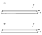
【解決手段】プロセスモジュール11のチャンバ17内に、円板状のシリコン基材43と、該シリコン基材43上に設けられた不織布44とを有するクリーニング基板45を搬入し、チャンバ17内を排気する排気システムによりチャンバ17内を真空引きすると共に、チャンバ17の壁面や構成部品の表面に付着しているパーティクルを剥離させて、チャンバ17内のパーティクルをクリーニング基板45の不織布44に入射させ、その後、不織布44内にパーティクルを捕捉したクリーニング基板45をチャンバ17内から搬出する。
【選択図】図2
Description
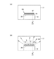
10 基板処理システム
11 プロセスモジュール
17 チャンバ
18 サセプタ
44 不織布
45,52,64 クリーニング基板
48,51 多孔質セラミックス
59 防水膜
60,68 洗浄剤
61 袋
67 金属薄膜
69 樹脂膜
Claims (17)
- 基板処理装置の処理室内をクリーニングするクリーニング基板であって、
前記処理室内の異物を除去する除去機構を備えることを特徴とするクリーニング基板。 - 前記除去機構はパーティクルを捕捉するパーティクル捕捉材からなることを特徴とする請求項1記載のクリーニング基板。
- 前記除去機構は水分を吸収する水分吸収材からなることを特徴とする請求項1記載のクリーニング基板。
- 前記水分吸収材は防水膜によって覆われることを特徴とする請求項3記載のクリーニング基板。
- 前記除去機構は、前記処理室内の付着物を洗浄する洗浄剤を被包する袋と、該袋を担持し、前記クリーニング基板が前記処理室内に配置された載置台に載置される際に当該クリーニング基板と当該載置台との間隙に供給されるガスの圧力を前記袋に伝達させるための複数の貫通孔が形成された基材とを有することを特徴とする請求項1記載のクリーニング基板。
- 前記除去機構は、前記処理室内の付着物を洗浄する洗浄剤を被包する袋と、該袋を担持する基材と、前記袋に被装された金属薄膜とを有することを特徴とする請求項1記載のクリーニング基板。
- 前記除去機構は、表面に前記処理室内の付着物を洗浄する揮発性の洗浄剤が塗布された基材と、該基材の表面を覆う樹脂膜とを有することを特徴とする請求項1記載のクリーニング基板。
- 基板処理装置の処理室内のクリーニング方法であって、
パーティクルを捕捉するパーティクル捕捉材を有するクリーニング基板を前記処理室内に搬入する搬入ステップと、
前記処理室内を真空引きして当該処理室内のパーティクルを排出する排出ステップと、
前記クリーニング基板を前記処理室内から搬出する搬出ステップとを有することを特徴とするクリーニング方法。 - 前記排出ステップでは、前記処理室内においてパーティクルの飛散を促進することを特徴とする請求項8記載のクリーニング方法。
- 前記搬出されたクリーニング基板におけるパーティクル捕捉材に捕捉されたパーティクルを除去する除去ステップを有することを特徴とする請求項8又は9記載のクリーニング方法。
- 基板処理装置の処理室内のクリーニング方法であって、
水分を吸収する水分吸収材を有するクリーニング基板を高温状態で前記処理室内に搬入する搬入ステップと、
前記搬入されたクリーニング基板を冷却すると共に前記処理室を加熱する温度調節ステップと、
当該クリーニング基板を前記処理室内から搬出する搬出ステップとを有することを特徴とするクリーニング方法。 - 基板処理装置の処理室内のクリーニング方法であって、
防水膜に覆われた、水分を吸収する水分吸収材を有するクリーニング基板を前記処理室内に搬入する搬入ステップと、
前記搬入されたクリーニング基板の防水膜をエッチングするエッチングステップと、
当該クリーニング基板を冷却すると共に前記処理室を加熱する温度調節ステップと、
当該クリーニング基板を前記処理室内から搬出する搬出ステップとを有することを特徴とするクリーニング方法。 - 前記搬出されたクリーニング基板における水分吸収材に吸収された水分を除去する除去ステップを有することを特徴とする請求項11又は12記載のクリーニング方法。
- 基板を収容する処理室と、該処理室内に配置されて前記基板を載置する載置台とを備え、前記載置台の上面には複数のガス供給孔が開口している基板処理装置における前記処理室内のクリーニング方法であって、
前記処理室内の付着物を洗浄する洗浄剤を被包する袋と、該袋を担持し、複数の貫通孔が形成された基材とを有するクリーニング基板を前記処理室内に搬入して前記載置台に載置する載置ステップと、
当該クリーニング基板と前記載置台との間隙にガスを高圧供給する高圧供給ステップと、
当該クリーニング基板を前記処理室内から搬出する搬出ステップとを有することを特徴とするクリーニング方法。 - 前記洗浄剤を中和する中和剤を被包する袋と、該袋を担持し、複数の貫通孔が形成された基材とを有する他のクリーニング基板を前記処理室内に搬入して前記載置台に載置する他の載置ステップと、
当該クリーニング基板と前記載置台との間隙にガスを高圧供給する他の高圧供給ステップと、
当該クリーニング基板を前記処理室内から搬出する他の搬出ステップとを有することを特徴とする請求項14記載のクリーニング方法。 - 基板を収容する処理室と、該処理室内に配置されて前記基板を載置する載置台とを備え、前記載置台は内部に直流電源に接続された電極板を有する基板処理装置における前記処理室内のクリーニング方法であって、
前記処理室内の付着物を洗浄する洗浄剤を被包する袋と、該袋を担持する基材と、前記袋に被装された金属薄膜とを有するクリーニング基板を前記処理室内に搬入して前記載置台に載置する載置ステップと、
前記電極板に直流電圧を印加する印加ステップと、
当該クリーニング基板を前記処理室内から搬出する搬出ステップとを有することを特徴とするクリーニング方法。 - 基板処理装置の処理室内のクリーニング方法であって、
表面に前記処理室内の付着物を洗浄する揮発性の洗浄剤が塗布された基材と、該基材の表面を覆う樹脂膜とを有するクリーニング基板を前記処理室内に搬入する搬入ステップと、
前記処理室内にプラズマを発生させる発生ステップと、
当該クリーニング基板を前記処理室内から搬出する搬出ステップとを有することを特徴とするクリーニング方法。
Priority Applications (3)
| Application Number | Priority Date | Filing Date | Title |
|---|---|---|---|
| JP2008083045A JP2009239013A (ja) | 2008-03-27 | 2008-03-27 | クリーニング基板及びクリーニング方法 |
| US12/408,888 US20090241992A1 (en) | 2008-03-27 | 2009-03-23 | Cleaning substrate and cleaning method |
| US13/454,695 US8647442B2 (en) | 2008-03-27 | 2012-04-24 | Cleaning substrate and cleaning method |
Applications Claiming Priority (1)
| Application Number | Priority Date | Filing Date | Title |
|---|---|---|---|
| JP2008083045A JP2009239013A (ja) | 2008-03-27 | 2008-03-27 | クリーニング基板及びクリーニング方法 |
Related Child Applications (1)
| Application Number | Title | Priority Date | Filing Date |
|---|---|---|---|
| JP2013151890A Division JP5658803B2 (ja) | 2013-07-22 | 2013-07-22 | クリーニング方法 |
Publications (1)
| Publication Number | Publication Date |
|---|---|
| JP2009239013A true JP2009239013A (ja) | 2009-10-15 |
Family
ID=41115280
Family Applications (1)
| Application Number | Title | Priority Date | Filing Date |
|---|---|---|---|
| JP2008083045A Pending JP2009239013A (ja) | 2008-03-27 | 2008-03-27 | クリーニング基板及びクリーニング方法 |
Country Status (2)
| Country | Link |
|---|---|
| US (2) | US20090241992A1 (ja) |
| JP (1) | JP2009239013A (ja) |
Cited By (4)
| Publication number | Priority date | Publication date | Assignee | Title |
|---|---|---|---|---|
| JP2013201248A (ja) * | 2012-03-23 | 2013-10-03 | Dainippon Screen Mfg Co Ltd | 基板収容容器および異物除去方法 |
| KR20150110338A (ko) * | 2014-03-24 | 2015-10-02 | 도쿄엘렉트론가부시키가이샤 | 종형 열처리 장치의 운전 방법, 기억 매체 및 종형 열처리 장치 |
| WO2017094388A1 (ja) * | 2015-11-30 | 2017-06-08 | 東京エレクトロン株式会社 | 基板処理装置のチャンバークリーニング方法 |
| WO2020045286A1 (ja) * | 2018-08-30 | 2020-03-05 | 株式会社クリエイティブテクノロジー | クリーニング装置 |
Families Citing this family (6)
| Publication number | Priority date | Publication date | Assignee | Title |
|---|---|---|---|---|
| US9579697B2 (en) * | 2012-12-06 | 2017-02-28 | Taiwan Semiconductor Manufacturing Co., Ltd. | System and method of cleaning FOUP |
| JP6812264B2 (ja) * | 2017-02-16 | 2021-01-13 | 東京エレクトロン株式会社 | 真空処理装置、及びメンテナンス装置 |
| WO2018204500A1 (en) * | 2017-05-02 | 2018-11-08 | Tokyo Electron Limited | Manufacturing methods to reduce surface particle impurities after a plasma process |
| US10766057B2 (en) * | 2017-12-28 | 2020-09-08 | Micron Technology, Inc. | Components and systems for cleaning a tool for forming a semiconductor device, and related methods |
| CN109254506B (zh) * | 2018-08-15 | 2021-10-15 | 上海华力集成电路制造有限公司 | 光刻胶剥离设备及其剥离方法 |
| DE102019131799A1 (de) * | 2019-11-25 | 2021-05-27 | Koenig & Bauer Ag | Bearbeitungsmaschine mit zumindest einer Reinigungsvorrichtung und Verfahren zur Reinigung |
Citations (2)
| Publication number | Priority date | Publication date | Assignee | Title |
|---|---|---|---|---|
| JPH0596057U (ja) * | 1992-05-27 | 1993-12-27 | 日新電機株式会社 | クリーニングウエーハ |
| JPH06252066A (ja) * | 1993-02-23 | 1994-09-09 | Toshiba Corp | 半導体製造装置と半導体装置の製造方法 |
Family Cites Families (8)
| Publication number | Priority date | Publication date | Assignee | Title |
|---|---|---|---|---|
| JPH06299349A (ja) | 1993-04-15 | 1994-10-25 | Nissin Electric Co Ltd | イオン注入装置 |
| US6079426A (en) * | 1997-07-02 | 2000-06-27 | Applied Materials, Inc. | Method and apparatus for determining the endpoint in a plasma cleaning process |
| US8012403B2 (en) * | 2001-09-14 | 2011-09-06 | Battelle Memorial Institute | Method for producing high purity low dielectric constant ceramic and hybrid ceramic films |
| US6630411B1 (en) * | 2002-05-07 | 2003-10-07 | Lsi Logic Corporation | Method and apparatus for removing water vapor as a byproduct of chemical reaction in a wafer processing chamber |
| JP2004063669A (ja) | 2002-07-26 | 2004-02-26 | Oki Electric Ind Co Ltd | 半導体製造装置クリーニングウエハとその製造方法、およびそれを用いたクリーニング方法 |
| JP4693571B2 (ja) | 2005-09-28 | 2011-06-01 | 株式会社クボタ | バックホー |
| WO2007087343A2 (en) * | 2006-01-25 | 2007-08-02 | Intematix Corporation | Solar modules with tracking and concentrating features |
| US20100112814A1 (en) * | 2006-09-06 | 2010-05-06 | Sowmya Krishnan | Pre-certified process chamber and method |
-
2008
- 2008-03-27 JP JP2008083045A patent/JP2009239013A/ja active Pending
-
2009
- 2009-03-23 US US12/408,888 patent/US20090241992A1/en not_active Abandoned
-
2012
- 2012-04-24 US US13/454,695 patent/US8647442B2/en active Active
Patent Citations (2)
| Publication number | Priority date | Publication date | Assignee | Title |
|---|---|---|---|---|
| JPH0596057U (ja) * | 1992-05-27 | 1993-12-27 | 日新電機株式会社 | クリーニングウエーハ |
| JPH06252066A (ja) * | 1993-02-23 | 1994-09-09 | Toshiba Corp | 半導体製造装置と半導体装置の製造方法 |
Cited By (8)
| Publication number | Priority date | Publication date | Assignee | Title |
|---|---|---|---|---|
| JP2013201248A (ja) * | 2012-03-23 | 2013-10-03 | Dainippon Screen Mfg Co Ltd | 基板収容容器および異物除去方法 |
| KR20150110338A (ko) * | 2014-03-24 | 2015-10-02 | 도쿄엘렉트론가부시키가이샤 | 종형 열처리 장치의 운전 방법, 기억 매체 및 종형 열처리 장치 |
| KR101896746B1 (ko) | 2014-03-24 | 2018-09-07 | 도쿄엘렉트론가부시키가이샤 | 종형 열처리 장치의 운전 방법, 기억 매체 및 종형 열처리 장치 |
| WO2017094388A1 (ja) * | 2015-11-30 | 2017-06-08 | 東京エレクトロン株式会社 | 基板処理装置のチャンバークリーニング方法 |
| JPWO2017094388A1 (ja) * | 2015-11-30 | 2018-09-13 | 東京エレクトロン株式会社 | 基板処理装置のチャンバークリーニング方法 |
| WO2020045286A1 (ja) * | 2018-08-30 | 2020-03-05 | 株式会社クリエイティブテクノロジー | クリーニング装置 |
| JPWO2020045286A1 (ja) * | 2018-08-30 | 2021-08-12 | 株式会社クリエイティブテクノロジー | クリーニング装置 |
| JP7350339B2 (ja) | 2018-08-30 | 2023-09-26 | 株式会社クリエイティブテクノロジー | クリーニング装置 |
Also Published As
| Publication number | Publication date |
|---|---|
| US20090241992A1 (en) | 2009-10-01 |
| US20120204904A1 (en) | 2012-08-16 |
| US8647442B2 (en) | 2014-02-11 |
Similar Documents
| Publication | Publication Date | Title |
|---|---|---|
| JP2009239013A (ja) | クリーニング基板及びクリーニング方法 | |
| US8236109B2 (en) | Component cleaning method and storage medium | |
| US7654010B2 (en) | Substrate processing system, substrate processing method, and storage medium | |
| KR101124745B1 (ko) | 기판 처리 장치의 진공 배기 방법 및 그를 위한 기판 처리 장치 | |
| CN101728243A (zh) | 基板清洗方法及装置 | |
| KR101310513B1 (ko) | 기판 세정 방법 | |
| JP2008186864A (ja) | ゲートバルブの洗浄方法及び基板処理システム | |
| JP4666575B2 (ja) | セラミック溶射部材の製造方法、該方法を実行するためのプログラム、記憶媒体、及びセラミック溶射部材 | |
| JP2010183005A (ja) | 搬送チャンバ及びパーティクル付着防止方法 | |
| US10643825B2 (en) | Particle generation preventing method and vacuum apparatus | |
| KR100900594B1 (ko) | 기판 처리 시스템, 기판 처리 방법 및 기억 매체 | |
| US20180204745A1 (en) | Substrate processing apparatus, substrate processing method and computer readable recording medium | |
| TWI398920B (zh) | Surface treatment of substrates | |
| US20100319726A1 (en) | Substrate preparation using megasonic coupling fluid meniscus | |
| JP4783094B2 (ja) | プラズマ処理用環状部品、プラズマ処理装置、及び外側環状部材 | |
| US6598314B1 (en) | Method of drying wafers | |
| US20060201910A1 (en) | Methods for removing extraneous amounts of molding material from a substrate | |
| JP5658803B2 (ja) | クリーニング方法 | |
| JP3244220B2 (ja) | 平板状物の乾燥方法および乾燥装置 | |
| US20220238346A1 (en) | Substrate processing apparatus, substrate processing method, and non-transitory computer-readable storage medium | |
| JP2003115519A (ja) | 半導体装置の製造方法、半導体製造装置、ロードロック室、基板収納ケース、ストッカ | |
| JP2008001101A (ja) | 余分量の成形材料を基板から除去する方法 | |
| JP2004079682A (ja) | 基板処理装置 | |
| TWI837947B (zh) | 半導體晶圓用乾冰洗淨裝置及半導體晶圓之洗淨方法 | |
| JP2001259412A (ja) | プラズマ処理装置 |
Legal Events
| Date | Code | Title | Description |
|---|---|---|---|
| A621 | Written request for application examination |
Free format text: JAPANESE INTERMEDIATE CODE: A621 Effective date: 20110308 |
|
| A131 | Notification of reasons for refusal |
Free format text: JAPANESE INTERMEDIATE CODE: A131 Effective date: 20130521 |
|
| A977 | Report on retrieval |
Free format text: JAPANESE INTERMEDIATE CODE: A971007 Effective date: 20130523 |
|
| A521 | Written amendment |
Free format text: JAPANESE INTERMEDIATE CODE: A523 Effective date: 20130722 |
|
| A02 | Decision of refusal |
Free format text: JAPANESE INTERMEDIATE CODE: A02 Effective date: 20131001 |