JP2009076540A - 半導体装置 - Google Patents
半導体装置 Download PDFInfo
- Publication number
- JP2009076540A JP2009076540A JP2007242011A JP2007242011A JP2009076540A JP 2009076540 A JP2009076540 A JP 2009076540A JP 2007242011 A JP2007242011 A JP 2007242011A JP 2007242011 A JP2007242011 A JP 2007242011A JP 2009076540 A JP2009076540 A JP 2009076540A
- Authority
- JP
- Japan
- Prior art keywords
- region
- base
- gate
- trench
- semiconductor device
- Prior art date
- Legal status (The legal status is an assumption and is not a legal conclusion. Google has not performed a legal analysis and makes no representation as to the accuracy of the status listed.)
- Pending
Links
- 239000004065 semiconductor Substances 0.000 title claims abstract description 19
- 239000000758 substrate Substances 0.000 claims description 7
- 230000002542 deteriorative effect Effects 0.000 abstract 1
- 239000010410 layer Substances 0.000 description 10
- 238000010586 diagram Methods 0.000 description 9
- 210000000746 body region Anatomy 0.000 description 8
- 239000011229 interlayer Substances 0.000 description 7
- XUIMIQQOPSSXEZ-UHFFFAOYSA-N Silicon Chemical compound [Si] XUIMIQQOPSSXEZ-UHFFFAOYSA-N 0.000 description 5
- 230000003071 parasitic effect Effects 0.000 description 5
- 229910052710 silicon Inorganic materials 0.000 description 5
- 239000010703 silicon Substances 0.000 description 5
- 230000015572 biosynthetic process Effects 0.000 description 4
- 238000003491 array Methods 0.000 description 3
- 239000000463 material Substances 0.000 description 3
- 230000007423 decrease Effects 0.000 description 2
- 239000002184 metal Substances 0.000 description 2
- 230000002093 peripheral effect Effects 0.000 description 2
- 238000009751 slip forming Methods 0.000 description 2
- 230000008094 contradictory effect Effects 0.000 description 1
- 230000000593 degrading effect Effects 0.000 description 1
- 230000001419 dependent effect Effects 0.000 description 1
- 238000009792 diffusion process Methods 0.000 description 1
- 230000000694 effects Effects 0.000 description 1
- 230000010354 integration Effects 0.000 description 1
- 238000005468 ion implantation Methods 0.000 description 1
Images


Classifications
-
- H—ELECTRICITY
- H01—ELECTRIC ELEMENTS
- H01L—SEMICONDUCTOR DEVICES NOT COVERED BY CLASS H10
- H01L29/00—Semiconductor devices adapted for rectifying, amplifying, oscillating or switching, or capacitors or resistors with at least one potential-jump barrier or surface barrier, e.g. PN junction depletion layer or carrier concentration layer; Details of semiconductor bodies or of electrodes thereof ; Multistep manufacturing processes therefor
- H01L29/66—Types of semiconductor device ; Multistep manufacturing processes therefor
- H01L29/68—Types of semiconductor device ; Multistep manufacturing processes therefor controllable by only the electric current supplied, or only the electric potential applied, to an electrode which does not carry the current to be rectified, amplified or switched
- H01L29/76—Unipolar devices, e.g. field effect transistors
- H01L29/772—Field effect transistors
- H01L29/78—Field effect transistors with field effect produced by an insulated gate
- H01L29/7801—DMOS transistors, i.e. MISFETs with a channel accommodating body or base region adjoining a drain drift region
- H01L29/7802—Vertical DMOS transistors, i.e. VDMOS transistors
- H01L29/7813—Vertical DMOS transistors, i.e. VDMOS transistors with trench gate electrode, e.g. UMOS transistors
-
- H—ELECTRICITY
- H01—ELECTRIC ELEMENTS
- H01L—SEMICONDUCTOR DEVICES NOT COVERED BY CLASS H10
- H01L27/00—Devices consisting of a plurality of semiconductor or other solid-state components formed in or on a common substrate
- H01L27/02—Devices consisting of a plurality of semiconductor or other solid-state components formed in or on a common substrate including semiconductor components specially adapted for rectifying, oscillating, amplifying or switching and having at least one potential-jump barrier or surface barrier; including integrated passive circuit elements with at least one potential-jump barrier or surface barrier
- H01L27/04—Devices consisting of a plurality of semiconductor or other solid-state components formed in or on a common substrate including semiconductor components specially adapted for rectifying, oscillating, amplifying or switching and having at least one potential-jump barrier or surface barrier; including integrated passive circuit elements with at least one potential-jump barrier or surface barrier the substrate being a semiconductor body
- H01L27/06—Devices consisting of a plurality of semiconductor or other solid-state components formed in or on a common substrate including semiconductor components specially adapted for rectifying, oscillating, amplifying or switching and having at least one potential-jump barrier or surface barrier; including integrated passive circuit elements with at least one potential-jump barrier or surface barrier the substrate being a semiconductor body including a plurality of individual components in a non-repetitive configuration
- H01L27/07—Devices consisting of a plurality of semiconductor or other solid-state components formed in or on a common substrate including semiconductor components specially adapted for rectifying, oscillating, amplifying or switching and having at least one potential-jump barrier or surface barrier; including integrated passive circuit elements with at least one potential-jump barrier or surface barrier the substrate being a semiconductor body including a plurality of individual components in a non-repetitive configuration the components having an active region in common
- H01L27/0705—Devices consisting of a plurality of semiconductor or other solid-state components formed in or on a common substrate including semiconductor components specially adapted for rectifying, oscillating, amplifying or switching and having at least one potential-jump barrier or surface barrier; including integrated passive circuit elements with at least one potential-jump barrier or surface barrier the substrate being a semiconductor body including a plurality of individual components in a non-repetitive configuration the components having an active region in common comprising components of the field effect type
- H01L27/0727—Devices consisting of a plurality of semiconductor or other solid-state components formed in or on a common substrate including semiconductor components specially adapted for rectifying, oscillating, amplifying or switching and having at least one potential-jump barrier or surface barrier; including integrated passive circuit elements with at least one potential-jump barrier or surface barrier the substrate being a semiconductor body including a plurality of individual components in a non-repetitive configuration the components having an active region in common comprising components of the field effect type in combination with diodes, or capacitors or resistors
-
- H—ELECTRICITY
- H01—ELECTRIC ELEMENTS
- H01L—SEMICONDUCTOR DEVICES NOT COVERED BY CLASS H10
- H01L29/00—Semiconductor devices adapted for rectifying, amplifying, oscillating or switching, or capacitors or resistors with at least one potential-jump barrier or surface barrier, e.g. PN junction depletion layer or carrier concentration layer; Details of semiconductor bodies or of electrodes thereof ; Multistep manufacturing processes therefor
- H01L29/02—Semiconductor bodies ; Multistep manufacturing processes therefor
- H01L29/06—Semiconductor bodies ; Multistep manufacturing processes therefor characterised by their shape; characterised by the shapes, relative sizes, or dispositions of the semiconductor regions ; characterised by the concentration or distribution of impurities within semiconductor regions
- H01L29/0684—Semiconductor bodies ; Multistep manufacturing processes therefor characterised by their shape; characterised by the shapes, relative sizes, or dispositions of the semiconductor regions ; characterised by the concentration or distribution of impurities within semiconductor regions characterised by the shape, relative sizes or dispositions of the semiconductor regions or junctions between the regions
- H01L29/0692—Surface layout
- H01L29/0696—Surface layout of cellular field-effect devices, e.g. multicellular DMOS transistors or IGBTs
-
- H—ELECTRICITY
- H01—ELECTRIC ELEMENTS
- H01L—SEMICONDUCTOR DEVICES NOT COVERED BY CLASS H10
- H01L29/00—Semiconductor devices adapted for rectifying, amplifying, oscillating or switching, or capacitors or resistors with at least one potential-jump barrier or surface barrier, e.g. PN junction depletion layer or carrier concentration layer; Details of semiconductor bodies or of electrodes thereof ; Multistep manufacturing processes therefor
- H01L29/66—Types of semiconductor device ; Multistep manufacturing processes therefor
- H01L29/68—Types of semiconductor device ; Multistep manufacturing processes therefor controllable by only the electric current supplied, or only the electric potential applied, to an electrode which does not carry the current to be rectified, amplified or switched
- H01L29/76—Unipolar devices, e.g. field effect transistors
- H01L29/772—Field effect transistors
- H01L29/78—Field effect transistors with field effect produced by an insulated gate
- H01L29/7801—DMOS transistors, i.e. MISFETs with a channel accommodating body or base region adjoining a drain drift region
- H01L29/7802—Vertical DMOS transistors, i.e. VDMOS transistors
- H01L29/7803—Vertical DMOS transistors, i.e. VDMOS transistors structurally associated with at least one other device
- H01L29/7808—Vertical DMOS transistors, i.e. VDMOS transistors structurally associated with at least one other device the other device being a breakdown diode, e.g. Zener diode
-
- H—ELECTRICITY
- H01—ELECTRIC ELEMENTS
- H01L—SEMICONDUCTOR DEVICES NOT COVERED BY CLASS H10
- H01L29/00—Semiconductor devices adapted for rectifying, amplifying, oscillating or switching, or capacitors or resistors with at least one potential-jump barrier or surface barrier, e.g. PN junction depletion layer or carrier concentration layer; Details of semiconductor bodies or of electrodes thereof ; Multistep manufacturing processes therefor
- H01L29/02—Semiconductor bodies ; Multistep manufacturing processes therefor
- H01L29/06—Semiconductor bodies ; Multistep manufacturing processes therefor characterised by their shape; characterised by the shapes, relative sizes, or dispositions of the semiconductor regions ; characterised by the concentration or distribution of impurities within semiconductor regions
- H01L29/10—Semiconductor bodies ; Multistep manufacturing processes therefor characterised by their shape; characterised by the shapes, relative sizes, or dispositions of the semiconductor regions ; characterised by the concentration or distribution of impurities within semiconductor regions with semiconductor regions connected to an electrode not carrying current to be rectified, amplified or switched and such electrode being part of a semiconductor device which comprises three or more electrodes
- H01L29/1095—Body region, i.e. base region, of DMOS transistors or IGBTs
Abstract
【解決手段】本発明の一態様に係る半導体装置は、縞状に交互に配置されたN+ソース領域4及びP+ベース領域5と、N+ソース領域4及びP+ベース領域5が延在する方向に交差するように、ストライプ状に配置された複数のゲートトレンチ7と、2つのゲートトレンチ7に接するように形成されたP+ベースダイオード領域6とを備える。
【選択図】図1
Description
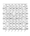
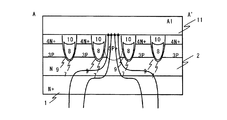
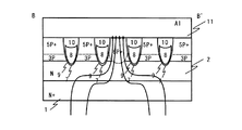
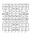
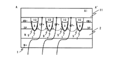
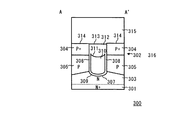
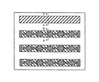
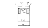
本発明の実施の形態1に係る半導体装置の構成について、図1〜図3を参照して説明する。図1は、本実施の形態に係る半導体装置の一例である、Nチャネルトレンチ埋め込み縦型MOSFETの表面レイアウトを示す図である。図2は、図1のA−A'断面図である。図3は、図1のB−B'断面図である。
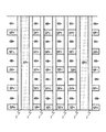
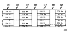
本発明の実施の形態2に係る半導体装置の構成について、図4を参照して説明する。図4は、本実施の形態に係る半導体装置の一例である、Nチャネルトレンチ埋め込み縦型MOSFETの表面レイアウトを示す図である。本実施の形態において、図1に示す実施の形態1と異なる点は、P+ベースダイオード領域6の形成位置である。なお、図4において、図1〜3と同様の構成要素には同一の符号を付し説明を省略する。
本発明の実施の形態3に係る半導体装置の構成について、図5を参照して説明する。図5は、本実施の形態に係る半導体装置の一例である、Nチャネルトレンチ埋め込み縦型MOSFETの表面レイアウトを示す図である。本実施の形態において、図1に示す実施の形態1と異なる点は、P+ベースダイオード領域6の形成位置である。なお、図5において、図1〜3と同様の構成要素には同一の符号を付し説明を省略する。
本発明の実施の形態4に係る半導体装置の構成について、図6を参照して説明する。図6は、本実施の形態に係る半導体装置の一例である、Nチャネルトレンチ埋め込み縦型MOSFETの表面レイアウトを示す図である。本実施の形態において、図1に示す実施の形態1と異なる点は、P+ベースダイオード領域6の形成位置である。なお、図6において、図1〜3と同様の構成要素には同一の符号を付し説明を省略する。
2 N型ドレイン領域
3 Pベース領域
4 N+ソース領域
5 P+ベース領域
6 P+ベースダイオード領域
7 ゲートトレンチ
8 ゲート電極
9 ゲート酸化膜
10 層間絶縁膜
11 ソース電極
Claims (7)
- 縞状に交互に配置されたN+ソース領域及びP+ベース領域と、
前記N+ソース領域及び前記P+ベース領域が延在する方向に交差するように、ストライプ状に配置された複数のゲートトレンチと、
2つの前記ゲートトレンチに接するように形成されたP+ベースダイオード領域と、
を備える半導体装置。 - 前記P+ベースダイオード領域の大きさは、少なくとも1つの前記N+ソース領域と2つのP+ベース領域に対応する大きさである請求項1に記載の半導体装置。
- 前記P+ベースダイオード領域は、隣接する2つの前記P+ベース領域と、当該2つのP+ベース領域間に形成された前記N+ソース領域とにわたって形成されている請求項1又は2に記載の半導体装置。
- 前記P+ベースダイオード領域は、前記P+ベース領域をまたぐように形成されている請求項1又は2に記載の半導体装置。
- 前記P+ベースダイオード領域は、2つの前記ゲートトレンチ間において、基板端から当該基板端の反対側の基板端にわたって形成されている請求項1、2に記載の半導体装置。
- 前記P+ベースダイオード領域は、前記複数のゲートトレンチにまたがって形成されている請求項1〜4のいずれか1項に記載の半導体装置。
- 前記ゲートトレンチ内に形成されたゲート電極と、
前記ゲート電極上に形成された絶縁膜とを備え、
前記ゲートトレンチは、前記ゲート電極、前記絶縁膜とで埋め込まれている請求項1〜6のいずれか1項に記載の半導体装置。
Priority Applications (3)
| Application Number | Priority Date | Filing Date | Title |
|---|---|---|---|
| JP2007242011A JP2009076540A (ja) | 2007-09-19 | 2007-09-19 | 半導体装置 |
| US12/232,074 US7956409B2 (en) | 2007-09-19 | 2008-09-10 | Semiconductor device having trench gate structure |
| CN2008101497393A CN101393915B (zh) | 2007-09-19 | 2008-09-19 | 具有沟槽栅极结构的半导体器件 |
Applications Claiming Priority (1)
| Application Number | Priority Date | Filing Date | Title |
|---|---|---|---|
| JP2007242011A JP2009076540A (ja) | 2007-09-19 | 2007-09-19 | 半導体装置 |
Publications (2)
| Publication Number | Publication Date |
|---|---|
| JP2009076540A true JP2009076540A (ja) | 2009-04-09 |
| JP2009076540A5 JP2009076540A5 (ja) | 2010-09-16 |
Family
ID=40453518
Family Applications (1)
| Application Number | Title | Priority Date | Filing Date |
|---|---|---|---|
| JP2007242011A Pending JP2009076540A (ja) | 2007-09-19 | 2007-09-19 | 半導体装置 |
Country Status (3)
| Country | Link |
|---|---|
| US (1) | US7956409B2 (ja) |
| JP (1) | JP2009076540A (ja) |
| CN (1) | CN101393915B (ja) |
Cited By (2)
| Publication number | Priority date | Publication date | Assignee | Title |
|---|---|---|---|---|
| US10312233B2 (en) | 2014-09-30 | 2019-06-04 | Mitsubishi Electric Corporation | Semiconductor device |
| US11189723B2 (en) | 2019-12-10 | 2021-11-30 | Fuji Electric Co., Ltd. | Semiconductor device |
Families Citing this family (4)
| Publication number | Priority date | Publication date | Assignee | Title |
|---|---|---|---|---|
| US9431484B2 (en) | 2011-07-29 | 2016-08-30 | Infineon Technologies Austria Ag | Vertical transistor with improved robustness |
| CN103904124B (zh) * | 2014-04-10 | 2016-08-17 | 电子科技大学 | 具有u型延伸栅的soi槽型ldmos器件 |
| US9905558B1 (en) * | 2016-12-22 | 2018-02-27 | Texas Instruments Incorporated | Conductivity modulated drain extended MOSFET |
| CN113632237B (zh) * | 2019-03-22 | 2022-09-13 | 日立能源瑞士股份公司 | 具有低传导损耗的反向传导绝缘栅功率半导体器件 |
Citations (3)
| Publication number | Priority date | Publication date | Assignee | Title |
|---|---|---|---|---|
| JPH09102607A (ja) * | 1995-06-02 | 1997-04-15 | Siliconix Inc | トレンチゲートパワーmosfet |
| JP2000031484A (ja) * | 1998-06-02 | 2000-01-28 | Siliconix Inc | 高セル密度のバ―チカルトレンチゲ―ト型mosfet |
| JP2006012967A (ja) * | 2004-06-23 | 2006-01-12 | Toshiba Corp | 半導体装置 |
Family Cites Families (4)
| Publication number | Priority date | Publication date | Assignee | Title |
|---|---|---|---|---|
| US5998837A (en) | 1995-06-02 | 1999-12-07 | Siliconix Incorporated | Trench-gated power MOSFET with protective diode having adjustable breakdown voltage |
| US6351009B1 (en) | 1999-03-01 | 2002-02-26 | Fairchild Semiconductor Corporation | MOS-gated device having a buried gate and process for forming same |
| US6413822B2 (en) * | 1999-04-22 | 2002-07-02 | Advanced Analogic Technologies, Inc. | Super-self-aligned fabrication process of trench-gate DMOS with overlying device layer |
| JP4059846B2 (ja) * | 2003-12-26 | 2008-03-12 | Necエレクトロニクス株式会社 | 半導体装置及びその製造方法 |
-
2007
- 2007-09-19 JP JP2007242011A patent/JP2009076540A/ja active Pending
-
2008
- 2008-09-10 US US12/232,074 patent/US7956409B2/en not_active Expired - Fee Related
- 2008-09-19 CN CN2008101497393A patent/CN101393915B/zh not_active Expired - Fee Related
Patent Citations (3)
| Publication number | Priority date | Publication date | Assignee | Title |
|---|---|---|---|---|
| JPH09102607A (ja) * | 1995-06-02 | 1997-04-15 | Siliconix Inc | トレンチゲートパワーmosfet |
| JP2000031484A (ja) * | 1998-06-02 | 2000-01-28 | Siliconix Inc | 高セル密度のバ―チカルトレンチゲ―ト型mosfet |
| JP2006012967A (ja) * | 2004-06-23 | 2006-01-12 | Toshiba Corp | 半導体装置 |
Cited By (2)
| Publication number | Priority date | Publication date | Assignee | Title |
|---|---|---|---|---|
| US10312233B2 (en) | 2014-09-30 | 2019-06-04 | Mitsubishi Electric Corporation | Semiconductor device |
| US11189723B2 (en) | 2019-12-10 | 2021-11-30 | Fuji Electric Co., Ltd. | Semiconductor device |
Also Published As
| Publication number | Publication date |
|---|---|
| US20090072300A1 (en) | 2009-03-19 |
| US7956409B2 (en) | 2011-06-07 |
| CN101393915A (zh) | 2009-03-25 |
| CN101393915B (zh) | 2011-12-14 |
Similar Documents
| Publication | Publication Date | Title |
|---|---|---|
| JP5511124B2 (ja) | 絶縁ゲート型半導体装置 | |
| JP5630114B2 (ja) | 炭化珪素半導体装置 | |
| JP5048273B2 (ja) | 絶縁ゲート型半導体装置 | |
| JP4609656B2 (ja) | トレンチ構造半導体装置 | |
| US8476702B2 (en) | Semiconductor device | |
| JP2008085188A (ja) | 絶縁ゲート型半導体装置 | |
| JP2008108962A (ja) | 半導体装置 | |
| US10249708B2 (en) | Semiconductor device | |
| JP2014187141A (ja) | 半導体装置 | |
| JP2009088385A (ja) | 半導体装置及びその製造方法 | |
| WO2016080322A1 (ja) | 半導体装置および半導体装置の製造方法 | |
| KR20080095768A (ko) | 반도체 장치 | |
| JP2009076540A (ja) | 半導体装置 | |
| US11362207B2 (en) | Semiconductor device | |
| JP2010232335A (ja) | 絶縁ゲートバイポーラトランジスタ | |
| US9257501B2 (en) | Semiconductor device | |
| JP2007317683A (ja) | 半導体装置 | |
| KR20180109719A (ko) | 반도체 장치 | |
| US20220013666A1 (en) | Semiconductor device | |
| JP4966351B2 (ja) | 半導体装置 | |
| JP6252022B2 (ja) | 半導体装置 | |
| JP4820899B2 (ja) | 半導体装置 | |
| JP4749665B2 (ja) | 半導体装置 | |
| JP2013033799A (ja) | 半導体装置 | |
| JP7147510B2 (ja) | スイッチング素子 |
Legal Events
| Date | Code | Title | Description |
|---|---|---|---|
| A621 | Written request for application examination |
Free format text: JAPANESE INTERMEDIATE CODE: A621 Effective date: 20100513 |
|
| A521 | Written amendment |
Free format text: JAPANESE INTERMEDIATE CODE: A523 Effective date: 20100803 |
|
| A977 | Report on retrieval |
Free format text: JAPANESE INTERMEDIATE CODE: A971007 Effective date: 20121031 |
|
| A131 | Notification of reasons for refusal |
Free format text: JAPANESE INTERMEDIATE CODE: A131 Effective date: 20121106 |
|
| A02 | Decision of refusal |
Free format text: JAPANESE INTERMEDIATE CODE: A02 Effective date: 20130604 |