JP2009076540A - Semiconductor device - Google Patents
Semiconductor device Download PDFInfo
- Publication number
- JP2009076540A JP2009076540A JP2007242011A JP2007242011A JP2009076540A JP 2009076540 A JP2009076540 A JP 2009076540A JP 2007242011 A JP2007242011 A JP 2007242011A JP 2007242011 A JP2007242011 A JP 2007242011A JP 2009076540 A JP2009076540 A JP 2009076540A
- Authority
- JP
- Japan
- Prior art keywords
- region
- base
- gate
- trench
- semiconductor device
- Prior art date
- Legal status (The legal status is an assumption and is not a legal conclusion. Google has not performed a legal analysis and makes no representation as to the accuracy of the status listed.)
- Pending
Links
- 239000004065 semiconductor Substances 0.000 title claims abstract description 19
- 239000000758 substrate Substances 0.000 claims description 7
- 230000002542 deteriorative effect Effects 0.000 abstract 1
- 239000010410 layer Substances 0.000 description 10
- 238000010586 diagram Methods 0.000 description 9
- 210000000746 body region Anatomy 0.000 description 8
- 239000011229 interlayer Substances 0.000 description 7
- XUIMIQQOPSSXEZ-UHFFFAOYSA-N Silicon Chemical compound [Si] XUIMIQQOPSSXEZ-UHFFFAOYSA-N 0.000 description 5
- 230000003071 parasitic effect Effects 0.000 description 5
- 229910052710 silicon Inorganic materials 0.000 description 5
- 239000010703 silicon Substances 0.000 description 5
- 230000015572 biosynthetic process Effects 0.000 description 4
- 238000003491 array Methods 0.000 description 3
- 239000000463 material Substances 0.000 description 3
- 230000007423 decrease Effects 0.000 description 2
- 239000002184 metal Substances 0.000 description 2
- 230000002093 peripheral effect Effects 0.000 description 2
- 238000009751 slip forming Methods 0.000 description 2
- 230000008094 contradictory effect Effects 0.000 description 1
- 230000000593 degrading effect Effects 0.000 description 1
- 230000001419 dependent effect Effects 0.000 description 1
- 238000009792 diffusion process Methods 0.000 description 1
- 230000000694 effects Effects 0.000 description 1
- 230000010354 integration Effects 0.000 description 1
- 238000005468 ion implantation Methods 0.000 description 1
Images


Classifications
-
- H—ELECTRICITY
- H01—ELECTRIC ELEMENTS
- H01L—SEMICONDUCTOR DEVICES NOT COVERED BY CLASS H10
- H01L29/00—Semiconductor devices adapted for rectifying, amplifying, oscillating or switching, or capacitors or resistors with at least one potential-jump barrier or surface barrier, e.g. PN junction depletion layer or carrier concentration layer; Details of semiconductor bodies or of electrodes thereof ; Multistep manufacturing processes therefor
- H01L29/66—Types of semiconductor device ; Multistep manufacturing processes therefor
- H01L29/68—Types of semiconductor device ; Multistep manufacturing processes therefor controllable by only the electric current supplied, or only the electric potential applied, to an electrode which does not carry the current to be rectified, amplified or switched
- H01L29/76—Unipolar devices, e.g. field effect transistors
- H01L29/772—Field effect transistors
- H01L29/78—Field effect transistors with field effect produced by an insulated gate
- H01L29/7801—DMOS transistors, i.e. MISFETs with a channel accommodating body or base region adjoining a drain drift region
- H01L29/7802—Vertical DMOS transistors, i.e. VDMOS transistors
- H01L29/7813—Vertical DMOS transistors, i.e. VDMOS transistors with trench gate electrode, e.g. UMOS transistors
-
- H—ELECTRICITY
- H01—ELECTRIC ELEMENTS
- H01L—SEMICONDUCTOR DEVICES NOT COVERED BY CLASS H10
- H01L27/00—Devices consisting of a plurality of semiconductor or other solid-state components formed in or on a common substrate
- H01L27/02—Devices consisting of a plurality of semiconductor or other solid-state components formed in or on a common substrate including semiconductor components specially adapted for rectifying, oscillating, amplifying or switching and having at least one potential-jump barrier or surface barrier; including integrated passive circuit elements with at least one potential-jump barrier or surface barrier
- H01L27/04—Devices consisting of a plurality of semiconductor or other solid-state components formed in or on a common substrate including semiconductor components specially adapted for rectifying, oscillating, amplifying or switching and having at least one potential-jump barrier or surface barrier; including integrated passive circuit elements with at least one potential-jump barrier or surface barrier the substrate being a semiconductor body
- H01L27/06—Devices consisting of a plurality of semiconductor or other solid-state components formed in or on a common substrate including semiconductor components specially adapted for rectifying, oscillating, amplifying or switching and having at least one potential-jump barrier or surface barrier; including integrated passive circuit elements with at least one potential-jump barrier or surface barrier the substrate being a semiconductor body including a plurality of individual components in a non-repetitive configuration
- H01L27/07—Devices consisting of a plurality of semiconductor or other solid-state components formed in or on a common substrate including semiconductor components specially adapted for rectifying, oscillating, amplifying or switching and having at least one potential-jump barrier or surface barrier; including integrated passive circuit elements with at least one potential-jump barrier or surface barrier the substrate being a semiconductor body including a plurality of individual components in a non-repetitive configuration the components having an active region in common
- H01L27/0705—Devices consisting of a plurality of semiconductor or other solid-state components formed in or on a common substrate including semiconductor components specially adapted for rectifying, oscillating, amplifying or switching and having at least one potential-jump barrier or surface barrier; including integrated passive circuit elements with at least one potential-jump barrier or surface barrier the substrate being a semiconductor body including a plurality of individual components in a non-repetitive configuration the components having an active region in common comprising components of the field effect type
- H01L27/0727—Devices consisting of a plurality of semiconductor or other solid-state components formed in or on a common substrate including semiconductor components specially adapted for rectifying, oscillating, amplifying or switching and having at least one potential-jump barrier or surface barrier; including integrated passive circuit elements with at least one potential-jump barrier or surface barrier the substrate being a semiconductor body including a plurality of individual components in a non-repetitive configuration the components having an active region in common comprising components of the field effect type in combination with diodes, or capacitors or resistors
-
- H—ELECTRICITY
- H01—ELECTRIC ELEMENTS
- H01L—SEMICONDUCTOR DEVICES NOT COVERED BY CLASS H10
- H01L29/00—Semiconductor devices adapted for rectifying, amplifying, oscillating or switching, or capacitors or resistors with at least one potential-jump barrier or surface barrier, e.g. PN junction depletion layer or carrier concentration layer; Details of semiconductor bodies or of electrodes thereof ; Multistep manufacturing processes therefor
- H01L29/02—Semiconductor bodies ; Multistep manufacturing processes therefor
- H01L29/06—Semiconductor bodies ; Multistep manufacturing processes therefor characterised by their shape; characterised by the shapes, relative sizes, or dispositions of the semiconductor regions ; characterised by the concentration or distribution of impurities within semiconductor regions
- H01L29/0684—Semiconductor bodies ; Multistep manufacturing processes therefor characterised by their shape; characterised by the shapes, relative sizes, or dispositions of the semiconductor regions ; characterised by the concentration or distribution of impurities within semiconductor regions characterised by the shape, relative sizes or dispositions of the semiconductor regions or junctions between the regions
- H01L29/0692—Surface layout
- H01L29/0696—Surface layout of cellular field-effect devices, e.g. multicellular DMOS transistors or IGBTs
-
- H—ELECTRICITY
- H01—ELECTRIC ELEMENTS
- H01L—SEMICONDUCTOR DEVICES NOT COVERED BY CLASS H10
- H01L29/00—Semiconductor devices adapted for rectifying, amplifying, oscillating or switching, or capacitors or resistors with at least one potential-jump barrier or surface barrier, e.g. PN junction depletion layer or carrier concentration layer; Details of semiconductor bodies or of electrodes thereof ; Multistep manufacturing processes therefor
- H01L29/66—Types of semiconductor device ; Multistep manufacturing processes therefor
- H01L29/68—Types of semiconductor device ; Multistep manufacturing processes therefor controllable by only the electric current supplied, or only the electric potential applied, to an electrode which does not carry the current to be rectified, amplified or switched
- H01L29/76—Unipolar devices, e.g. field effect transistors
- H01L29/772—Field effect transistors
- H01L29/78—Field effect transistors with field effect produced by an insulated gate
- H01L29/7801—DMOS transistors, i.e. MISFETs with a channel accommodating body or base region adjoining a drain drift region
- H01L29/7802—Vertical DMOS transistors, i.e. VDMOS transistors
- H01L29/7803—Vertical DMOS transistors, i.e. VDMOS transistors structurally associated with at least one other device
- H01L29/7808—Vertical DMOS transistors, i.e. VDMOS transistors structurally associated with at least one other device the other device being a breakdown diode, e.g. Zener diode
-
- H—ELECTRICITY
- H01—ELECTRIC ELEMENTS
- H01L—SEMICONDUCTOR DEVICES NOT COVERED BY CLASS H10
- H01L29/00—Semiconductor devices adapted for rectifying, amplifying, oscillating or switching, or capacitors or resistors with at least one potential-jump barrier or surface barrier, e.g. PN junction depletion layer or carrier concentration layer; Details of semiconductor bodies or of electrodes thereof ; Multistep manufacturing processes therefor
- H01L29/02—Semiconductor bodies ; Multistep manufacturing processes therefor
- H01L29/06—Semiconductor bodies ; Multistep manufacturing processes therefor characterised by their shape; characterised by the shapes, relative sizes, or dispositions of the semiconductor regions ; characterised by the concentration or distribution of impurities within semiconductor regions
- H01L29/10—Semiconductor bodies ; Multistep manufacturing processes therefor characterised by their shape; characterised by the shapes, relative sizes, or dispositions of the semiconductor regions ; characterised by the concentration or distribution of impurities within semiconductor regions with semiconductor regions connected to an electrode not carrying current to be rectified, amplified or switched and such electrode being part of a semiconductor device which comprises three or more electrodes
- H01L29/1095—Body region, i.e. base region, of DMOS transistors or IGBTs
Abstract
Description
本発明は半導体装置に関し、特に、ストライプトレンチ構造を有する、トレンチ埋め込み縦型MOSFETに関する。 The present invention relates to a semiconductor device, and more particularly to a trench-embedded vertical MOSFET having a stripe trench structure.
ストライプトレンチ構造のMOSFETにおいて、アバランシェ耐量はP+ベース領域の幅、間隔、P+ベース領域の総面積により左右される。P+ベース領域の間隔が狭いほどアバランシェ耐量は向上する。しかし、その反面チャネル領域が減少するため、MOSFETの性能指数の一つであるオン抵抗(Ron)が増加し性能が悪化する。従って、P+ベース領域の幅を確保(チャネル領域を確保)して、Ronを低減しつつ、アバランシェ耐量を向上させる構造が要求されている。 In MOSFET stripe trench structure, the avalanche withstand capability is dependent P + base region having a width, spacing, the total area of P + base region. The avalanche resistance is improved as the interval between the P + base regions is narrower. However, since the channel region decreases, the on-resistance (Ron), which is one of the figure of merit of the MOSFET, increases and the performance deteriorates. Therefore, there is a demand for a structure that increases the avalanche resistance while securing the width of the P + base region (securing the channel region) and reducing Ron.
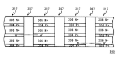
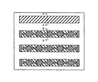
従来のストライプトレンチ構造を有するトレンチ埋め込み縦型MOSFETの一例が、特許文献1に記載されている。図9〜11を参照して、特許文献1に記載の従来のNチャネルトレンチ埋め込み縦型MOSFET300の構造について説明する。図9は、特許文献1に記載のMOSFET300の構造を示す平面図である。図10は図9のA−A'断面図、図11は図9のB−B'断面図である。
An example of a trench-embedded vertical MOSFET having a conventional stripe trench structure is described in
図9〜11に示すように、ドープされたN+基体301上にはドープされた上側層302が配置されている。上側層302はドレイン領域303とP型ウェル305を形成している。図10に示すように、上側層302中にはP+本体領域304が形成されている。P+本体領域304は、ゲートトレンチ307によって互いに分離されている。一方、図11に示すように、上側層302中には、イオン注入と拡散によってN+ソース領域306が形成されている。N+ソース領域306は、ゲートトレンチ307によって分離されている。
As shown in FIGS. 9-11, a doped
ゲートトレンチ307中には、導電ゲート材料310と誘電層312とが形成されている。この導電ゲート材料310と誘電層312によって、ゲートトレンチ307は埋め込まれ、誘電層312の表面とP+本体領域304の表面314とが略共通の平面となる。そして、表面314上には、金属層315が蒸着されている。金属層315により、P+本体領域304とN+ソース領域306とのコンタクトが形成される。
A conductive gate material 310 and a
図9に示すように、MOSFET300は、P+本体領域304とN+ソース領域306とが交互に配置された複数のアレイ317を含む。各アレイ317は、ゲートトレンチ307に隣接して配置され、次のアレイ317と分離されている。図9中、ゲートトレンチ307間に配置されているアレイ317において、縦寸法はP+本体領域304よりもN+ソース領域306のほうが広く形成されている。この構造により、ゲートトレンチ307とソース領域306が接する面においてチャネルが形成され、性能指数の一つであるRonが決定される。さらに、本構造のようにゲートトレンチ307と、導電ゲート材料310と誘電層312によって表面314とほぼ共通の平面に形成することにより、ゲートトレンチ307間を狭くすることができる。このため、同一チップ面積での、上述したチャネル領域を高密度に形成することが可能となり、性能を向上することができる。
As shown in FIG. 9,
また、特許文献2には、従来のストライプトレンチ構造を有するMOSFETの例が記載されている。図12〜15に、特許文献2に記載の従来のMOSFETの構造が示される。図12、13は、特許文献2に記載のMOSFETの平面構造を示す図である。図14は図12、13に示されるA−A'断面図、図15はB−B'断面図である。図に示すように、特許文献2に記載のMOSFETは、ストライプトレンチ構造を有するが、ゲートトレンチ埋め込み構造ではない。さらに、DeepP+領域が、ゲートトレンチと平行に形成されている。
しかしながら、特許文献1に記載の従来の構造では、P+本体領域304の幅、間隔により、アバランシェ耐量の最適値が存在する。アバランシェ耐量を最適化するためには、P+本体領域304の幅を大きく、間隔を狭くすることが必要となる。このため、N+ソース領域306が狭くなってしまい、チャネル領域が減少してしまい、Ronが増大する。つまり、性能(Ron)を重視する場合にはアバランシェ耐量が不足し、アバランシェ耐量を確保すると性能(Ron)が悪化するといった、相反関係となる。
However, in the conventional structure described in
また、特許文献2に記載の構造では、集積度を上げ、性能を(Ron)を低減させるためのトレンチ間隔が、DeepP+領域の幅(面積)によって制限される。このため、トレンチ間隔を狭くすることができないという問題が生じる。
In the structure disclosed in
本発明の一態様に係る半導体装置は、縞状に交互に配置されたN+ソース領域及びP+ベース領域と、前記N+ソース領域及び前記P+ベース領域が延在する方向に交差するように、ストライプ状に配置された複数のゲートトレンチと、2つの前記ゲートトレンチに接するように形成されたP+ベースダイオード領域とを備えるものである。これにより、チャネル長を減少させることがないため、性能を低下させる(Ronを増大させる)ことがない。また、アバランシェ電流をP+ベースダイオード領域に集中させることができるため、素子の破壊を防止することができ、アバランシェ耐量を確保することが可能となる。 In the semiconductor device according to one embodiment of the present invention, the N + source regions and the P + base regions that are alternately arranged in a stripe shape intersect with the extending direction of the N + source region and the P + base region. And a plurality of gate trenches arranged in stripes, and a P + base diode region formed so as to be in contact with the two gate trenches. Thereby, since the channel length is not reduced, the performance is not deteriorated (Ron is not increased). In addition, since the avalanche current can be concentrated in the P + base diode region, the element can be prevented from being destroyed and the avalanche resistance can be ensured.
本発明によれば、性能を低下させる(Ronを増大させる)ことなく、アバランシェ耐量を確保することが可能なストライプトレンチ構造を有する、トレンチ埋め込み縦型MOSFETを提供することができる。 According to the present invention, it is possible to provide a trench-embedded vertical MOSFET having a stripe trench structure capable of ensuring an avalanche resistance without degrading performance (increasing Ron).
実施の形態1.
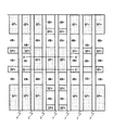
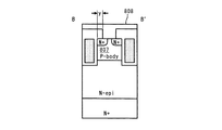
本発明の実施の形態1に係る半導体装置の構成について、図1〜図3を参照して説明する。図1は、本実施の形態に係る半導体装置の一例である、Nチャネルトレンチ埋め込み縦型MOSFETの表面レイアウトを示す図である。図2は、図1のA−A'断面図である。図3は、図1のB−B'断面図である。
The configuration of the semiconductor device according to the first embodiment of the present invention will be described with reference to FIGS. FIG. 1 is a diagram showing a surface layout of an N-channel trench-embedded vertical MOSFET that is an example of a semiconductor device according to the present embodiment. 2 is a cross-sectional view taken along line AA ′ of FIG. 3 is a cross-sectional view taken along the line BB ′ of FIG.
図1に示すように、本実施の形態に係るMOSFETは、ストライプ状に配置されたゲートトレンチ7を有している。ゲートトレンチ7は、セル領域において複数形成されている。なお、これらのゲートトレンチ7は周辺領域で互いに連結され1つのトレンチとなる場合もある。また、複数のゲートトレンチ7が、周辺領域でも連結されず、複数のままの場合もある。
As shown in FIG. 1, the MOSFET according to the present embodiment has
ゲートトレンチ7間には、N+ソース領域4とP+ベース領域5とが形成されている。N+ソース領域4とP+ベース領域5とは、ゲートトレンチ7に略直交する方向に、交互に形成されている。すなわち、図1において、横方向にN+ソース領域4とP+ベース領域5とが交互に縞状に形成されており、縦方向にゲートトレンチ7が形成されている。換言すると、本実施の形態に係るMOSFETは、P+ベース領域5とN+ソース領域4とが交互に配置された複数のアレイを含む。これらのアレイは、ゲートトレンチ7に隣接して配置されている。つまり、各アレイは、ゲートトレンチ7によって次のアレイから分離されている。
An N + source region 4 and a P + base region 5 are formed between the
各アレイの中で、任意のN+ソース領域4とP+ベース領域5の部分がP+ベースダイオード領域6として形成されている。例えば、図1中、左から1つ目と2つ目のゲートトレンチ7間(左から2つ目のアレイ)に、2つのP+ベースダイオード領域6が形成されている。
In each array, an arbitrary N + source region 4 and a portion of P + base region 5 are formed as P + base diode region 6. For example, in FIG. 1, two P + base diode regions 6 are formed between the first and
本実施の形態においては、P+ベースダイオード領域6は、1つのN+ソース領域4と2つのP+ベース領域5に対応するサイズとなっている。例えば、図1に示すように、左から2つ目のアレイにおいて、一番下のP+ベース領域5と次のP+ベース領域5の間に1つのN+ソース領域4を挟んだ領域に対応して、P+ベースダイオード領域6が形成されている。 In the present embodiment, the P + base diode region 6 has a size corresponding to one N + source region 4 and two P + base regions 5. For example, as shown in FIG. 1, in the second array from the left, a region in which one N + source region 4 is sandwiched between the bottom P + base region 5 and the next P + base region 5. Correspondingly, a P + base diode region 6 is formed.
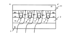
図2に示すように、N型シリコン基板1上には、N型ドレイン領域2が形成されている。また、N型ドレイン領域2の上には、Pベース領域3が形成されている。ゲートトレンチ7は、Pベース領域3を分断するように形成されている。ゲートトレンチ7内には、ゲート酸化膜9、ゲート電極8、層間絶縁膜10が形成されている。ゲートトレンチ7は、ゲート酸化膜9、ゲート電極8、層間絶縁膜10により埋め込まれている。また、層間絶縁膜10の表面は、シリコン表面とほぼ同一平面となっている。
As shown in FIG. 2, an N-
Pベース領域3上には、N+ベース領域4が形成されている。また、N+ベース領域4上には、ソース電極11が形成されている。N+ベース領域4は、ソース電極11とコンタクトされている。ソース電極11は、例えば、Alからなる。また、Pベース領域3中の所定の部分には、P+ベースダイオード領域6が形成されている。
On the P base region 3, an N + base region 4 is formed. A
一方、図3に示すように、B−B'断面においてもA−A'断面と同様に、N型シリコン基板1上には、N型ドレイン領域2が形成されている。また、N型ドレイン領域2の上には、Pベース領域3が形成されている。ゲートトレンチ7は、Pベース領域3を分断するように形成されている。ゲートトレンチ7内には、ゲート酸化膜9、ゲート電極8、層間絶縁膜10が形成されている。ゲートトレンチ7は、ゲート酸化膜9、ゲート電極8、層間絶縁膜10により埋め込まれている。また、層間絶縁膜10の表面は、シリコン表面とほぼ同一平面となっている。
On the other hand, as shown in FIG. 3, an N-
Pベース領域3上には、P+ベース領域5が形成されている。また、P+ベース領域5上には、ソース電極11が形成されている。P+ベース領域5は、ソース電極11とコンタクトされている。同様に、Pベース領域3中の所定の部分には、P+ベースダイオード領域6が形成されている。
A P + base region 5 is formed on the P base region 3. A
図1に示すように、ゲートトレンチ7とN+ベース領域4とが接する面において、チャネルが形成され、性能指数の一つであるRonが決定される。上述したように、ゲートトレンチ7を埋め込み、ソース電極11と絶縁することによりゲートトレンチ間隔を小さくすることができる。これにより、高密度化が可能となり、Ronの低減が可能となる。
As shown in FIG. 1, a channel is formed on the surface where the
本発明においては、P+ベース領域5の幅を広げ、間隔を狭くすることでアバランシェ耐量を確保するのではなく、ゲートトレンチ7間にP+ベースダイオード領域6を形成している。これにより、図2、3の矢印で示すように、P+ベースダイオード領域6にアバランシェ電流を集中させることができ、アバランシェ耐量を確保することができる。また、チャネル長を減少させることがないため、Ronが増大することもない。
In the present invention, the P + base diode region 6 is formed between the
図16に示した従来構造では、P+ベース領域5の幅、間隔が最適でないと、アバランシェ電流が任意のセル部のチャネル形成部流れてしまう。このため、寄生トランジスタがオンとなり、素子が破壊される場合があった。 In the conventional structure shown in FIG. 16, if the width and interval of the P + base region 5 are not optimum, an avalanche current flows through the channel forming portion of an arbitrary cell portion. For this reason, the parasitic transistor is turned on, and the element may be destroyed.
しかしながら、本発明によれば、図2及び図3に示すように、P+ベースダイオード領域6を形成することで、セル部のP+ベース領域5よりも深いP+ベース領域を形成することができる。これにより、アバランシェ電流をP+ベースダイオード領域6に集中させることができる。これにより、寄生トランジスタをオンさせることなく、素子の破壊を防止することが可能となる。 However, according to the present invention, as shown in FIGS. 2 and 3, by forming the P + base diode region 6, it is possible to form a P + base region deeper than the P + base region 5 of the cell portion. it can. Thereby, the avalanche current can be concentrated on the P + base diode region 6. Thereby, it is possible to prevent the element from being destroyed without turning on the parasitic transistor.
また、図1に示すように、本実施の形態に係るMOSFETでは、P+ベースダイオード領域6は、任意のP+ベース領域5とその隣のP+ベース領域5の間に1つのN+ソース領域4を挟んだ領域に対応して形成されている。従って、当該上下のP+ベース領域5間の領域にマスクパターンが形成されないようにしたマスクを用いることで、P+ベースダイオード領域6を形成することができる。このため、従来のマスクパターンのうち、P+ベースダイオード領域6に対応する当該上下のP+ベース領域5間の領域のマスクパターンを反転させるだけでよく、マスクパターンを容易に形成することができる。 As shown in FIG. 1, in the MOSFET according to the present embodiment, the P + base diode region 6 includes one N + source between an arbitrary P + base region 5 and the adjacent P + base region 5. It is formed corresponding to a region sandwiching the region 4. Therefore, the P + base diode region 6 can be formed by using a mask in which a mask pattern is not formed in the region between the upper and lower P + base regions 5. For this reason, it is only necessary to invert the mask pattern in the region between the upper and lower P + base regions 5 corresponding to the P + base diode region 6 in the conventional mask pattern, and the mask pattern can be easily formed. .
実施の形態2.
本発明の実施の形態2に係る半導体装置の構成について、図4を参照して説明する。図4は、本実施の形態に係る半導体装置の一例である、Nチャネルトレンチ埋め込み縦型MOSFETの表面レイアウトを示す図である。本実施の形態において、図1に示す実施の形態1と異なる点は、P+ベースダイオード領域6の形成位置である。なお、図4において、図1〜3と同様の構成要素には同一の符号を付し説明を省略する。
The configuration of the semiconductor device according to the second embodiment of the present invention will be described with reference to FIG. FIG. 4 is a diagram showing a surface layout of an N-channel trench-embedded vertical MOSFET that is an example of the semiconductor device according to the present embodiment. The present embodiment is different from the first embodiment shown in FIG. 1 in the formation position of the P + base diode region 6. In FIG. 4, the same components as those in FIGS.
実施の形態1では、P+ベースダイオード領域6を、任意の2つのP+ベース領域5と、当該2つのP+ベース領域5に挟まれたN+ソース領域4の部分に形成していた。本実施の形態においては、P+ベースダイオード領域6を、1つのP+ベース領域5をまたぐように形成している。 In the first embodiment, the P + base diode region 6 is formed in an arbitrary two P + base regions 5 and a portion of the N + source region 4 sandwiched between the two P + base regions 5. In the present embodiment, the P + base diode region 6 is formed so as to straddle one P + base region 5.
具体的には、図4に示すように、本実施の形態に係るMOSFETは、実施の形態1と同様に、ストライプ状に配置されたゲートトレンチ7を有している。ゲートトレンチ7間には、N+ソース領域4とP+ベース領域5とが形成されている。N+ソース領域4とP+ベース領域5とは、ゲートトレンチ7に略直交する方向に、交互に配置される。
Specifically, as shown in FIG. 4, the MOSFET according to the present embodiment has
そして、図4中、左から1つ目と2つ目のゲートトレンチ7間に、2つのP+ベースダイオード領域6が形成されている。本実施の形態においては、P+ベースダイオード領域6は、1つのN+ソース領域4と2つのP+ベース領域5に対応するサイズとなっている。また、図4に示すように、左から2つ目のアレイにおいて、P+ベースダイオード領域6は、一番下のN+ソース領域4の一部と、当該一番下のN+ソース領域4隣接するP+ベース領域5と、そのP+ベース領域5に隣接するN+ソース領域4の一部に対応して、連続して形成されている。すなわち、下から2番目のP+ベース領域5をまたぐように、P+ベースダイオード領域6が形成されている。なお、本実施の形態に係るMOSFETの他の構成については、図1〜3で示したものと略同一である。
In FIG. 4, two P + base diode regions 6 are formed between the first and
このように、P+ベースダイオード領域6を、P+ベース領域5をまたぐように形成した場合でも、実施の形態1のように、アバランシェ電流をP+ベースダイオード領域6に集中させることができる。これにより、寄生トランジスタをオンさせることなく、素子の破壊を防止することが可能となる。すなわち、P+ベースダイオード領域6の形成位置は、限定されたものではなく、部分的に配置することで何ら変わりない効果を得ることが可能となる。 Thus, even when the P + base diode region 6 is formed so as to straddle the P + base region 5, the avalanche current can be concentrated on the P + base diode region 6 as in the first embodiment. Thereby, it is possible to prevent the element from being destroyed without turning on the parasitic transistor. That is, the formation position of the P + base diode region 6 is not limited, and it is possible to obtain an effect that does not change at all by being partially arranged.
実施の形態3.
本発明の実施の形態3に係る半導体装置の構成について、図5を参照して説明する。図5は、本実施の形態に係る半導体装置の一例である、Nチャネルトレンチ埋め込み縦型MOSFETの表面レイアウトを示す図である。本実施の形態において、図1に示す実施の形態1と異なる点は、P+ベースダイオード領域6の形成位置である。なお、図5において、図1〜3と同様の構成要素には同一の符号を付し説明を省略する。
Embodiment 3 FIG.
The configuration of the semiconductor device according to the third embodiment of the present invention will be described with reference to FIG. FIG. 5 is a diagram showing a surface layout of an N-channel trench buried vertical MOSFET as an example of the semiconductor device according to the present embodiment. The present embodiment is different from the first embodiment shown in FIG. 1 in the formation position of the P + base diode region 6. In FIG. 5, the same components as those in FIGS.
図5に示すように、本実施の形態においては、P+ベースダイオード領域6は、任意の隣接する2つのゲートトレンチ7間に、当該ゲートトレンチ7が延在する方向と平行にチップ端からつなげて形成されている。
As shown in FIG. 5, in this embodiment, the P + base diode region 6 is connected between any two
具体的には、図5に示すように、本実施の形態に係るMOSFETは、実施の形態1と同様に、ストライプ状に配置されたゲートトレンチ7を有している。ゲートトレンチ7間には、N+ソース領域4とP+ベース領域5とが形成されている。N+ソース領域4とP+ベース領域5とは、ゲートトレンチ7に略直交する方向に、交互に配置される。そして、図4中、左から1つ目と2つ目のゲートトレンチ7間の略全面に、1つのP+ベースダイオード領域6が形成されている。図5に示すように、左から2つ目のアレイにおいて、P+ベースダイオード領域6は、下側のチップ端から上側のチップ端まで連続して形成されている。なお、本実施の形態に係るMOSFETの他の構成については、図1〜3で示したものと略同一である。
Specifically, as shown in FIG. 5, the MOSFET according to the present embodiment has
このように、P+ベースダイオード領域6を、2つのゲートトレンチ7間に連続して形成した場合でも、実施の形態1のように、アバランシェ電流をP+ベースダイオード領域6に集中させることができる。これにより、寄生トランジスタをオンさせることなく、素子の破壊を防止することが可能となる。
Thus, even when the P + base diode region 6 is continuously formed between the two
また、図5に示すように、本実施の形態に係るMOSFETでは、P+ベースダイオード領域6は、任意の隣接する2つのゲートトレンチ7間に、当該ゲートトレンチ7が延在する方向と平行にチップ端からつなげて形成されている。従って、当該ゲートトレンチ7間の領域にマスクパターンが形成されないようにしたマスクを用いることで、P+ベースダイオード領域6を形成することができる。このため、従来のマスクパターンのうち、P+ベースダイオード領域6に対応する当該ゲートトレンチ7間の領域のマスクパターンを反転させるだけでよく、マスクパターンを容易に形成することができる。
Further, as shown in FIG. 5, in the MOSFET according to the present embodiment, the P + base diode region 6 is parallel to the direction in which the
実施の形態4.
本発明の実施の形態4に係る半導体装置の構成について、図6を参照して説明する。図6は、本実施の形態に係る半導体装置の一例である、Nチャネルトレンチ埋め込み縦型MOSFETの表面レイアウトを示す図である。本実施の形態において、図1に示す実施の形態1と異なる点は、P+ベースダイオード領域6の形成位置である。なお、図6において、図1〜3と同様の構成要素には同一の符号を付し説明を省略する。
Embodiment 4 FIG.
The configuration of the semiconductor device according to the fourth embodiment of the present invention will be described with reference to FIG. FIG. 6 is a diagram showing a surface layout of an N-channel trench-embedded vertical MOSFET that is an example of the semiconductor device according to the present embodiment. The present embodiment is different from the first embodiment shown in FIG. 1 in the formation position of the P + base diode region 6. In FIG. 6, the same components as those in FIGS.
本実施の形態においては、P+ベースダイオード領域6は、複数のゲートトレンチ7にまたがって形成されている。すなわち、図6に示すように、本実施の形態に係るMOSFETは、実施の形態1と同様に、ストライプ状に配置されたゲートトレンチ7を有している。ゲートトレンチ7間には、N+ソース領域4とP+ベース領域5とが形成されている。N+ソース領域4とP+ベース領域5とは、ゲートトレンチ7に略直交する方向に、交互に配置される。
In the present embodiment, the P + base diode region 6 is formed across a plurality of
そして、例えば、図6中、左から2つ目と3つ目、3つ目と4つ目、4つ目と5つ目のそれぞれのゲートトレンチ7間にP+ベースダイオード領域6がまたがって形成されている。すなわち、P+ベースダイオード領域6は、左から3つ目のアレイ、4つ目のアレイ、5つ目のアレイにまたがって形成されている。また、本実施の形態においては、P+ベースダイオード領域6は、1つのN+ソース領域4と2つのP+ベース領域5に対応するサイズとなっている。例えば、図6に示すように、左から4つ目のアレイにおいて、下から3つ目のP+ベース領域5と次のP+ベース領域5の間に1つのN+ソース領域4を挟んだ領域に対応して、P+ベースダイオード領域6が形成されている。なお、本実施の形態に係るMOSFETの他の構成については、図1〜3で示したものと略同一である。
For example, in FIG. 6, the P + base diode region 6 extends between the second, third, third, fourth, fourth, and
このように、P+ベースダイオード領域6を、複数のゲートトレンチ7にまたがって形成した場合でも、実施の形態1のように、アバランシェ電流をP+ベースダイオード領域6に集中させることができる。これにより、寄生トランジスタをオンさせることなく、素子の破壊を防止することが可能となる。また、図7、8に示すように、P+ベースダイオード領域6を、複数のゲートトレンチ7にまたがって形成しているため、各P+ベースダイオード領域6に流れるアバランシェ電流を小さくすることができる。
Thus, even when the P + base diode region 6 is formed across the plurality of
また、図6に示すように、本実施の形態に係るMOSFETでは、P+ベースダイオード領域6は、任意のP+ベース領域5とその隣のP+ベース領域5の行間に1つのN+ソース領域4を挟んだ領域に対応し、複数のゲートトレンチ7間にまたがって形成されている。従って、この領域にマスクパターンが形成されないようにしたマスクを用いることで、P+ベースダイオード領域6を形成することができる。このため、従来のマスクパターンのうち、P+ベースダイオード領域6に対応する当該上下のP+ベース領域5行間で、複数のゲートトレンチ7にまたがった領域のマスクパターンを反転させるだけでよく、マスクパターンを容易に形成することができる。
As shown in FIG. 6, in the MOSFET according to the present embodiment, the P + base diode region 6 includes one N + source between a row of an arbitrary P + base region 5 and the adjacent P + base region 5. Corresponding to a region sandwiching the region 4, it is formed across a plurality of
以上説明したように、本発明によれば、性能を低下させることなく(オン抵抗Ronを増大させることなく)、相反するアバランシェ耐量も向上することが可能となる。 As described above, according to the present invention, it is possible to improve the contradictory avalanche resistance without reducing the performance (without increasing the on-resistance Ron).
1 N型シリコン基板1
2 N型ドレイン領域
3 Pベース領域
4 N+ソース領域
5 P+ベース領域
6 P+ベースダイオード領域
7 ゲートトレンチ
8 ゲート電極
9 ゲート酸化膜
10 層間絶縁膜
11 ソース電極
1 N-
2 N-
Claims (7)
前記N+ソース領域及び前記P+ベース領域が延在する方向に交差するように、ストライプ状に配置された複数のゲートトレンチと、
2つの前記ゲートトレンチに接するように形成されたP+ベースダイオード領域と、
を備える半導体装置。 N + source regions and P + base regions alternately arranged in a stripe pattern;
A plurality of gate trenches arranged in stripes so as to intersect in a direction in which the N + source region and the P + base region extend;
A P + base diode region formed in contact with the two gate trenches;
A semiconductor device comprising:
前記ゲート電極上に形成された絶縁膜とを備え、
前記ゲートトレンチは、前記ゲート電極、前記絶縁膜とで埋め込まれている請求項1〜6のいずれか1項に記載の半導体装置。 A gate electrode formed in the gate trench;
An insulating film formed on the gate electrode;
The semiconductor device according to claim 1, wherein the gate trench is embedded with the gate electrode and the insulating film.
Priority Applications (3)
| Application Number | Priority Date | Filing Date | Title |
|---|---|---|---|
| JP2007242011A JP2009076540A (en) | 2007-09-19 | 2007-09-19 | Semiconductor device |
| US12/232,074 US7956409B2 (en) | 2007-09-19 | 2008-09-10 | Semiconductor device having trench gate structure |
| CN2008101497393A CN101393915B (en) | 2007-09-19 | 2008-09-19 | Semiconductor device having trench gate structure |
Applications Claiming Priority (1)
| Application Number | Priority Date | Filing Date | Title |
|---|---|---|---|
| JP2007242011A JP2009076540A (en) | 2007-09-19 | 2007-09-19 | Semiconductor device |
Publications (2)
| Publication Number | Publication Date |
|---|---|
| JP2009076540A true JP2009076540A (en) | 2009-04-09 |
| JP2009076540A5 JP2009076540A5 (en) | 2010-09-16 |
Family
ID=40453518
Family Applications (1)
| Application Number | Title | Priority Date | Filing Date |
|---|---|---|---|
| JP2007242011A Pending JP2009076540A (en) | 2007-09-19 | 2007-09-19 | Semiconductor device |
Country Status (3)
| Country | Link |
|---|---|
| US (1) | US7956409B2 (en) |
| JP (1) | JP2009076540A (en) |
| CN (1) | CN101393915B (en) |
Cited By (2)
| Publication number | Priority date | Publication date | Assignee | Title |
|---|---|---|---|---|
| US10312233B2 (en) | 2014-09-30 | 2019-06-04 | Mitsubishi Electric Corporation | Semiconductor device |
| US11189723B2 (en) | 2019-12-10 | 2021-11-30 | Fuji Electric Co., Ltd. | Semiconductor device |
Families Citing this family (4)
| Publication number | Priority date | Publication date | Assignee | Title |
|---|---|---|---|---|
| US9431484B2 (en) | 2011-07-29 | 2016-08-30 | Infineon Technologies Austria Ag | Vertical transistor with improved robustness |
| CN103904124B (en) * | 2014-04-10 | 2016-08-17 | 电子科技大学 | There is the SOI grooved LDMOS device of U-shaped extension grid |
| US9905558B1 (en) * | 2016-12-22 | 2018-02-27 | Texas Instruments Incorporated | Conductivity modulated drain extended MOSFET |
| CN113632237B (en) * | 2019-03-22 | 2022-09-13 | 日立能源瑞士股份公司 | Reverse conducting insulated gate power semiconductor device with low conduction loss |
Citations (3)
| Publication number | Priority date | Publication date | Assignee | Title |
|---|---|---|---|---|
| JPH09102607A (en) * | 1995-06-02 | 1997-04-15 | Siliconix Inc | Trench gate power mosfet |
| JP2000031484A (en) * | 1998-06-02 | 2000-01-28 | Siliconix Inc | Vertical trench gate type mosfet with high cell density |
| JP2006012967A (en) * | 2004-06-23 | 2006-01-12 | Toshiba Corp | Semiconductor device |
Family Cites Families (4)
| Publication number | Priority date | Publication date | Assignee | Title |
|---|---|---|---|---|
| US5998837A (en) | 1995-06-02 | 1999-12-07 | Siliconix Incorporated | Trench-gated power MOSFET with protective diode having adjustable breakdown voltage |
| US6351009B1 (en) | 1999-03-01 | 2002-02-26 | Fairchild Semiconductor Corporation | MOS-gated device having a buried gate and process for forming same |
| US6413822B2 (en) * | 1999-04-22 | 2002-07-02 | Advanced Analogic Technologies, Inc. | Super-self-aligned fabrication process of trench-gate DMOS with overlying device layer |
| JP4059846B2 (en) * | 2003-12-26 | 2008-03-12 | Necエレクトロニクス株式会社 | Semiconductor device and manufacturing method thereof |
-
2007
- 2007-09-19 JP JP2007242011A patent/JP2009076540A/en active Pending
-
2008
- 2008-09-10 US US12/232,074 patent/US7956409B2/en not_active Expired - Fee Related
- 2008-09-19 CN CN2008101497393A patent/CN101393915B/en not_active Expired - Fee Related
Patent Citations (3)
| Publication number | Priority date | Publication date | Assignee | Title |
|---|---|---|---|---|
| JPH09102607A (en) * | 1995-06-02 | 1997-04-15 | Siliconix Inc | Trench gate power mosfet |
| JP2000031484A (en) * | 1998-06-02 | 2000-01-28 | Siliconix Inc | Vertical trench gate type mosfet with high cell density |
| JP2006012967A (en) * | 2004-06-23 | 2006-01-12 | Toshiba Corp | Semiconductor device |
Cited By (2)
| Publication number | Priority date | Publication date | Assignee | Title |
|---|---|---|---|---|
| US10312233B2 (en) | 2014-09-30 | 2019-06-04 | Mitsubishi Electric Corporation | Semiconductor device |
| US11189723B2 (en) | 2019-12-10 | 2021-11-30 | Fuji Electric Co., Ltd. | Semiconductor device |
Also Published As
| Publication number | Publication date |
|---|---|
| US7956409B2 (en) | 2011-06-07 |
| CN101393915B (en) | 2011-12-14 |
| US20090072300A1 (en) | 2009-03-19 |
| CN101393915A (en) | 2009-03-25 |
Similar Documents
| Publication | Publication Date | Title |
|---|---|---|
| JP5511124B2 (en) | Insulated gate semiconductor device | |
| JP5630114B2 (en) | Silicon carbide semiconductor device | |
| JP5048273B2 (en) | Insulated gate semiconductor device | |
| JP4609656B2 (en) | Trench structure semiconductor device | |
| US8476702B2 (en) | Semiconductor device | |
| JP2008085188A (en) | Insulated gate semiconductor device | |
| JP2008108962A (en) | Semiconductor device | |
| US10249708B2 (en) | Semiconductor device | |
| JP2014187141A (en) | Semiconductor device | |
| JP2009088385A (en) | Semiconductor device and method of manufacturing the same | |
| WO2016080322A1 (en) | Semiconductor device and method for manufacturing semiconductor device | |
| KR20080095768A (en) | Semiconductor device | |
| JP2009076540A (en) | Semiconductor device | |
| US11362207B2 (en) | Semiconductor device | |
| JP2010232335A (en) | Insulated gate bipolar transistor | |
| US9257501B2 (en) | Semiconductor device | |
| JP2007317683A (en) | Semiconductor device | |
| KR20180109719A (en) | Semiconductor device | |
| US20220013666A1 (en) | Semiconductor device | |
| JP4966351B2 (en) | Semiconductor device | |
| JP6252022B2 (en) | Semiconductor device | |
| JP4820899B2 (en) | Semiconductor device | |
| JP4749665B2 (en) | Semiconductor device | |
| JP2013033799A (en) | Semiconductor device | |
| JP5465837B2 (en) | Semiconductor device |
Legal Events
| Date | Code | Title | Description |
|---|---|---|---|
| A621 | Written request for application examination |
Free format text: JAPANESE INTERMEDIATE CODE: A621 Effective date: 20100513 |
|
| A521 | Written amendment |
Free format text: JAPANESE INTERMEDIATE CODE: A523 Effective date: 20100803 |
|
| A977 | Report on retrieval |
Free format text: JAPANESE INTERMEDIATE CODE: A971007 Effective date: 20121031 |
|
| A131 | Notification of reasons for refusal |
Free format text: JAPANESE INTERMEDIATE CODE: A131 Effective date: 20121106 |
|
| A02 | Decision of refusal |
Free format text: JAPANESE INTERMEDIATE CODE: A02 Effective date: 20130604 |