JP2009038368A - Semiconductor device, electronic instrument, and method of manufacturing semiconductor device - Google Patents
Semiconductor device, electronic instrument, and method of manufacturing semiconductor device Download PDFInfo
- Publication number
- JP2009038368A JP2009038368A JP2008179747A JP2008179747A JP2009038368A JP 2009038368 A JP2009038368 A JP 2009038368A JP 2008179747 A JP2008179747 A JP 2008179747A JP 2008179747 A JP2008179747 A JP 2008179747A JP 2009038368 A JP2009038368 A JP 2009038368A
- Authority
- JP
- Japan
- Prior art keywords
- layer
- single crystal
- crystal semiconductor
- insulating layer
- substrate
- Prior art date
- Legal status (The legal status is an assumption and is not a legal conclusion. Google has not performed a legal analysis and makes no representation as to the accuracy of the status listed.)
- Withdrawn
Links
- 239000004065 semiconductor Substances 0.000 title claims abstract description 369
- 238000004519 manufacturing process Methods 0.000 title claims abstract description 28
- 239000000758 substrate Substances 0.000 claims abstract description 167
- 239000013078 crystal Substances 0.000 claims description 238
- 239000012535 impurity Substances 0.000 claims description 73
- 238000000034 method Methods 0.000 claims description 49
- 230000000295 complement effect Effects 0.000 claims description 21
- 230000005684 electric field Effects 0.000 claims description 6
- 230000010354 integration Effects 0.000 abstract description 16
- 238000010030 laminating Methods 0.000 abstract 1
- 239000010410 layer Substances 0.000 description 450
- 239000000463 material Substances 0.000 description 35
- 238000010438 heat treatment Methods 0.000 description 33
- XUIMIQQOPSSXEZ-UHFFFAOYSA-N Silicon Chemical group [Si] XUIMIQQOPSSXEZ-UHFFFAOYSA-N 0.000 description 23
- 239000011521 glass Substances 0.000 description 23
- 229910052710 silicon Inorganic materials 0.000 description 22
- 239000010703 silicon Substances 0.000 description 22
- 229910052581 Si3N4 Inorganic materials 0.000 description 21
- 230000008569 process Effects 0.000 description 21
- 238000000926 separation method Methods 0.000 description 21
- HQVNEWCFYHHQES-UHFFFAOYSA-N silicon nitride Chemical compound N12[Si]34N5[Si]62N3[Si]51N64 HQVNEWCFYHHQES-UHFFFAOYSA-N 0.000 description 21
- 239000010408 film Substances 0.000 description 20
- 150000002500 ions Chemical class 0.000 description 20
- VYPSYNLAJGMNEJ-UHFFFAOYSA-N Silicium dioxide Chemical compound O=[Si]=O VYPSYNLAJGMNEJ-UHFFFAOYSA-N 0.000 description 19
- 239000007789 gas Substances 0.000 description 19
- 229910052814 silicon oxide Inorganic materials 0.000 description 17
- IJGRMHOSHXDMSA-UHFFFAOYSA-N Atomic nitrogen Chemical compound N#N IJGRMHOSHXDMSA-UHFFFAOYSA-N 0.000 description 14
- 230000015572 biosynthetic process Effects 0.000 description 14
- ZOXJGFHDIHLPTG-UHFFFAOYSA-N Boron Chemical compound [B] ZOXJGFHDIHLPTG-UHFFFAOYSA-N 0.000 description 13
- 229910052796 boron Inorganic materials 0.000 description 13
- 238000005229 chemical vapour deposition Methods 0.000 description 13
- 239000001257 hydrogen Substances 0.000 description 12
- 229910052739 hydrogen Inorganic materials 0.000 description 12
- 239000004973 liquid crystal related substance Substances 0.000 description 12
- 238000005530 etching Methods 0.000 description 11
- 230000004888 barrier function Effects 0.000 description 10
- -1 fluorine ions Chemical class 0.000 description 10
- 239000011347 resin Substances 0.000 description 10
- 229920005989 resin Polymers 0.000 description 10
- PXHVJJICTQNCMI-UHFFFAOYSA-N Nickel Chemical compound [Ni] PXHVJJICTQNCMI-UHFFFAOYSA-N 0.000 description 9
- 229910052782 aluminium Inorganic materials 0.000 description 9
- XAGFODPZIPBFFR-UHFFFAOYSA-N aluminium Chemical compound [Al] XAGFODPZIPBFFR-UHFFFAOYSA-N 0.000 description 9
- QVGXLLKOCUKJST-UHFFFAOYSA-N atomic oxygen Chemical compound [O] QVGXLLKOCUKJST-UHFFFAOYSA-N 0.000 description 9
- 238000001312 dry etching Methods 0.000 description 9
- 239000001301 oxygen Substances 0.000 description 9
- 229910052760 oxygen Inorganic materials 0.000 description 9
- 239000011810 insulating material Substances 0.000 description 8
- 239000011241 protective layer Substances 0.000 description 8
- 239000003990 capacitor Substances 0.000 description 7
- 229910052731 fluorine Inorganic materials 0.000 description 7
- 239000011737 fluorine Substances 0.000 description 7
- 230000006870 function Effects 0.000 description 7
- 239000011261 inert gas Substances 0.000 description 7
- 229910052757 nitrogen Inorganic materials 0.000 description 7
- XKRFYHLGVUSROY-UHFFFAOYSA-N Argon Chemical compound [Ar] XKRFYHLGVUSROY-UHFFFAOYSA-N 0.000 description 6
- UFHFLCQGNIYNRP-UHFFFAOYSA-N Hydrogen Chemical compound [H][H] UFHFLCQGNIYNRP-UHFFFAOYSA-N 0.000 description 6
- 229910052786 argon Inorganic materials 0.000 description 6
- 239000000460 chlorine Substances 0.000 description 6
- 239000011651 chromium Substances 0.000 description 6
- 150000001875 compounds Chemical class 0.000 description 6
- 239000010949 copper Substances 0.000 description 6
- KPUWHANPEXNPJT-UHFFFAOYSA-N disiloxane Chemical class [SiH3]O[SiH3] KPUWHANPEXNPJT-UHFFFAOYSA-N 0.000 description 6
- 238000010884 ion-beam technique Methods 0.000 description 6
- 238000001020 plasma etching Methods 0.000 description 6
- BASFCYQUMIYNBI-UHFFFAOYSA-N platinum Chemical compound [Pt] BASFCYQUMIYNBI-UHFFFAOYSA-N 0.000 description 6
- 238000005498 polishing Methods 0.000 description 6
- 238000004544 sputter deposition Methods 0.000 description 6
- 239000010936 titanium Substances 0.000 description 6
- GYHNNYVSQQEPJS-UHFFFAOYSA-N Gallium Chemical compound [Ga] GYHNNYVSQQEPJS-UHFFFAOYSA-N 0.000 description 5
- OAICVXFJPJFONN-UHFFFAOYSA-N Phosphorus Chemical compound [P] OAICVXFJPJFONN-UHFFFAOYSA-N 0.000 description 5
- 230000008859 change Effects 0.000 description 5
- 229910052733 gallium Inorganic materials 0.000 description 5
- 229910021421 monocrystalline silicon Inorganic materials 0.000 description 5
- 229910052698 phosphorus Inorganic materials 0.000 description 5
- 239000011574 phosphorus Substances 0.000 description 5
- 239000002356 single layer Substances 0.000 description 5
- 239000000126 substance Substances 0.000 description 5
- OKTJSMMVPCPJKN-UHFFFAOYSA-N Carbon Chemical compound [C] OKTJSMMVPCPJKN-UHFFFAOYSA-N 0.000 description 4
- YCKRFDGAMUMZLT-UHFFFAOYSA-N Fluorine atom Chemical compound [F] YCKRFDGAMUMZLT-UHFFFAOYSA-N 0.000 description 4
- 239000004642 Polyimide Substances 0.000 description 4
- 239000000956 alloy Substances 0.000 description 4
- 229910052799 carbon Inorganic materials 0.000 description 4
- PMHQVHHXPFUNSP-UHFFFAOYSA-M copper(1+);methylsulfanylmethane;bromide Chemical compound Br[Cu].CSC PMHQVHHXPFUNSP-UHFFFAOYSA-M 0.000 description 4
- 230000007547 defect Effects 0.000 description 4
- 238000001704 evaporation Methods 0.000 description 4
- 229910052736 halogen Inorganic materials 0.000 description 4
- 229910052734 helium Inorganic materials 0.000 description 4
- 229910003437 indium oxide Inorganic materials 0.000 description 4
- PJXISJQVUVHSOJ-UHFFFAOYSA-N indium(iii) oxide Chemical compound [O-2].[O-2].[O-2].[In+3].[In+3] PJXISJQVUVHSOJ-UHFFFAOYSA-N 0.000 description 4
- AMGQUBHHOARCQH-UHFFFAOYSA-N indium;oxotin Chemical compound [In].[Sn]=O AMGQUBHHOARCQH-UHFFFAOYSA-N 0.000 description 4
- 239000000203 mixture Substances 0.000 description 4
- 239000010955 niobium Substances 0.000 description 4
- 125000000962 organic group Chemical group 0.000 description 4
- 150000001282 organosilanes Chemical class 0.000 description 4
- 238000000059 patterning Methods 0.000 description 4
- 229920001721 polyimide Polymers 0.000 description 4
- 238000003825 pressing Methods 0.000 description 4
- ZAMOUSCENKQFHK-UHFFFAOYSA-N Chlorine atom Chemical compound [Cl] ZAMOUSCENKQFHK-UHFFFAOYSA-N 0.000 description 3
- VYZAMTAEIAYCRO-UHFFFAOYSA-N Chromium Chemical compound [Cr] VYZAMTAEIAYCRO-UHFFFAOYSA-N 0.000 description 3
- RYGMFSIKBFXOCR-UHFFFAOYSA-N Copper Chemical compound [Cu] RYGMFSIKBFXOCR-UHFFFAOYSA-N 0.000 description 3
- ZOKXTWBITQBERF-UHFFFAOYSA-N Molybdenum Chemical compound [Mo] ZOKXTWBITQBERF-UHFFFAOYSA-N 0.000 description 3
- BLRPTPMANUNPDV-UHFFFAOYSA-N Silane Chemical compound [SiH4] BLRPTPMANUNPDV-UHFFFAOYSA-N 0.000 description 3
- RTAQQCXQSZGOHL-UHFFFAOYSA-N Titanium Chemical compound [Ti] RTAQQCXQSZGOHL-UHFFFAOYSA-N 0.000 description 3
- XLOMVQKBTHCTTD-UHFFFAOYSA-N Zinc monoxide Chemical compound [Zn]=O XLOMVQKBTHCTTD-UHFFFAOYSA-N 0.000 description 3
- 125000004429 atom Chemical group 0.000 description 3
- 229910052801 chlorine Inorganic materials 0.000 description 3
- 229910052804 chromium Inorganic materials 0.000 description 3
- 238000000576 coating method Methods 0.000 description 3
- 229910052802 copper Inorganic materials 0.000 description 3
- 238000009826 distribution Methods 0.000 description 3
- 238000005468 ion implantation Methods 0.000 description 3
- 229910052751 metal Inorganic materials 0.000 description 3
- 239000002184 metal Substances 0.000 description 3
- 229910052750 molybdenum Inorganic materials 0.000 description 3
- 239000011733 molybdenum Substances 0.000 description 3
- 229910052759 nickel Inorganic materials 0.000 description 3
- 150000004767 nitrides Chemical class 0.000 description 3
- 238000004806 packaging method and process Methods 0.000 description 3
- 229910000077 silane Inorganic materials 0.000 description 3
- 229910052715 tantalum Inorganic materials 0.000 description 3
- GUVRBAGPIYLISA-UHFFFAOYSA-N tantalum atom Chemical compound [Ta] GUVRBAGPIYLISA-UHFFFAOYSA-N 0.000 description 3
- 229910052719 titanium Inorganic materials 0.000 description 3
- WFKWXMTUELFFGS-UHFFFAOYSA-N tungsten Chemical compound [W] WFKWXMTUELFFGS-UHFFFAOYSA-N 0.000 description 3
- 229910052721 tungsten Inorganic materials 0.000 description 3
- 239000010937 tungsten Substances 0.000 description 3
- 238000001039 wet etching Methods 0.000 description 3
- YVTHLONGBIQYBO-UHFFFAOYSA-N zinc indium(3+) oxygen(2-) Chemical compound [O--].[Zn++].[In+3] YVTHLONGBIQYBO-UHFFFAOYSA-N 0.000 description 3
- WZJUBBHODHNQPW-UHFFFAOYSA-N 2,4,6,8-tetramethyl-1,3,5,7,2$l^{3},4$l^{3},6$l^{3},8$l^{3}-tetraoxatetrasilocane Chemical compound C[Si]1O[Si](C)O[Si](C)O[Si](C)O1 WZJUBBHODHNQPW-UHFFFAOYSA-N 0.000 description 2
- JBRZTFJDHDCESZ-UHFFFAOYSA-N AsGa Chemical compound [As]#[Ga] JBRZTFJDHDCESZ-UHFFFAOYSA-N 0.000 description 2
- 102100040844 Dual specificity protein kinase CLK2 Human genes 0.000 description 2
- 229910001218 Gallium arsenide Inorganic materials 0.000 description 2
- 101000749291 Homo sapiens Dual specificity protein kinase CLK2 Proteins 0.000 description 2
- GPXJNWSHGFTCBW-UHFFFAOYSA-N Indium phosphide Chemical compound [In]#P GPXJNWSHGFTCBW-UHFFFAOYSA-N 0.000 description 2
- 229910052779 Neodymium Inorganic materials 0.000 description 2
- XYFCBTPGUUZFHI-UHFFFAOYSA-N Phosphine Chemical compound P XYFCBTPGUUZFHI-UHFFFAOYSA-N 0.000 description 2
- 239000004952 Polyamide Substances 0.000 description 2
- BQCADISMDOOEFD-UHFFFAOYSA-N Silver Chemical compound [Ag] BQCADISMDOOEFD-UHFFFAOYSA-N 0.000 description 2
- 229910002808 Si–O–Si Inorganic materials 0.000 description 2
- BOTDANWDWHJENH-UHFFFAOYSA-N Tetraethyl orthosilicate Chemical compound CCO[Si](OCC)(OCC)OCC BOTDANWDWHJENH-UHFFFAOYSA-N 0.000 description 2
- ATJFFYVFTNAWJD-UHFFFAOYSA-N Tin Chemical compound [Sn] ATJFFYVFTNAWJD-UHFFFAOYSA-N 0.000 description 2
- GWEVSGVZZGPLCZ-UHFFFAOYSA-N Titan oxide Chemical compound O=[Ti]=O GWEVSGVZZGPLCZ-UHFFFAOYSA-N 0.000 description 2
- 230000003213 activating effect Effects 0.000 description 2
- 230000004913 activation Effects 0.000 description 2
- 125000000217 alkyl group Chemical group 0.000 description 2
- 229910045601 alloy Inorganic materials 0.000 description 2
- 239000005407 aluminoborosilicate glass Substances 0.000 description 2
- 239000005354 aluminosilicate glass Substances 0.000 description 2
- UBSJOWMHLJZVDJ-UHFFFAOYSA-N aluminum neodymium Chemical compound [Al].[Nd] UBSJOWMHLJZVDJ-UHFFFAOYSA-N 0.000 description 2
- 150000001408 amides Chemical class 0.000 description 2
- 238000004458 analytical method Methods 0.000 description 2
- 125000003118 aryl group Chemical group 0.000 description 2
- 239000012298 atmosphere Substances 0.000 description 2
- 229910052788 barium Inorganic materials 0.000 description 2
- DSAJWYNOEDNPEQ-UHFFFAOYSA-N barium atom Chemical compound [Ba] DSAJWYNOEDNPEQ-UHFFFAOYSA-N 0.000 description 2
- UMIVXZPTRXBADB-UHFFFAOYSA-N benzocyclobutene Chemical compound C1=CC=C2CCC2=C1 UMIVXZPTRXBADB-UHFFFAOYSA-N 0.000 description 2
- 239000005388 borosilicate glass Substances 0.000 description 2
- 230000001413 cellular effect Effects 0.000 description 2
- 239000000919 ceramic Substances 0.000 description 2
- 229910017052 cobalt Inorganic materials 0.000 description 2
- 239000010941 cobalt Substances 0.000 description 2
- GUTLYIVDDKVIGB-UHFFFAOYSA-N cobalt atom Chemical compound [Co] GUTLYIVDDKVIGB-UHFFFAOYSA-N 0.000 description 2
- 238000004891 communication Methods 0.000 description 2
- 229920001940 conductive polymer Polymers 0.000 description 2
- ZOCHARZZJNPSEU-UHFFFAOYSA-N diboron Chemical compound B#B ZOCHARZZJNPSEU-UHFFFAOYSA-N 0.000 description 2
- 238000001678 elastic recoil detection analysis Methods 0.000 description 2
- 125000001153 fluoro group Chemical group F* 0.000 description 2
- 235000013305 food Nutrition 0.000 description 2
- 229910052732 germanium Inorganic materials 0.000 description 2
- GNPVGFCGXDBREM-UHFFFAOYSA-N germanium atom Chemical compound [Ge] GNPVGFCGXDBREM-UHFFFAOYSA-N 0.000 description 2
- 239000010931 gold Substances 0.000 description 2
- 229910052738 indium Inorganic materials 0.000 description 2
- APFVFJFRJDLVQX-UHFFFAOYSA-N indium atom Chemical compound [In] APFVFJFRJDLVQX-UHFFFAOYSA-N 0.000 description 2
- 238000007689 inspection Methods 0.000 description 2
- 239000011777 magnesium Substances 0.000 description 2
- 238000007726 management method Methods 0.000 description 2
- QEFYFXOXNSNQGX-UHFFFAOYSA-N neodymium atom Chemical compound [Nd] QEFYFXOXNSNQGX-UHFFFAOYSA-N 0.000 description 2
- 229910052758 niobium Inorganic materials 0.000 description 2
- GUCVJGMIXFAOAE-UHFFFAOYSA-N niobium atom Chemical compound [Nb] GUCVJGMIXFAOAE-UHFFFAOYSA-N 0.000 description 2
- QJGQUHMNIGDVPM-UHFFFAOYSA-N nitrogen group Chemical group [N] QJGQUHMNIGDVPM-UHFFFAOYSA-N 0.000 description 2
- QGLKJKCYBOYXKC-UHFFFAOYSA-N nonaoxidotritungsten Chemical compound O=[W]1(=O)O[W](=O)(=O)O[W](=O)(=O)O1 QGLKJKCYBOYXKC-UHFFFAOYSA-N 0.000 description 2
- HMMGMWAXVFQUOA-UHFFFAOYSA-N octamethylcyclotetrasiloxane Chemical compound C[Si]1(C)O[Si](C)(C)O[Si](C)(C)O[Si](C)(C)O1 HMMGMWAXVFQUOA-UHFFFAOYSA-N 0.000 description 2
- 230000010355 oscillation Effects 0.000 description 2
- TWNQGVIAIRXVLR-UHFFFAOYSA-N oxo(oxoalumanyloxy)alumane Chemical compound O=[Al]O[Al]=O TWNQGVIAIRXVLR-UHFFFAOYSA-N 0.000 description 2
- 238000000206 photolithography Methods 0.000 description 2
- 238000009832 plasma treatment Methods 0.000 description 2
- 229910052697 platinum Inorganic materials 0.000 description 2
- 229920000058 polyacrylate Polymers 0.000 description 2
- 229920002647 polyamide Polymers 0.000 description 2
- 229920001709 polysilazane Polymers 0.000 description 2
- 239000010453 quartz Substances 0.000 description 2
- 238000005001 rutherford backscattering spectroscopy Methods 0.000 description 2
- 229910052594 sapphire Inorganic materials 0.000 description 2
- 239000010980 sapphire Substances 0.000 description 2
- 238000007789 sealing Methods 0.000 description 2
- 229910052709 silver Inorganic materials 0.000 description 2
- 239000004332 silver Substances 0.000 description 2
- 125000001424 substituent group Chemical group 0.000 description 2
- 230000003746 surface roughness Effects 0.000 description 2
- 238000004381 surface treatment Methods 0.000 description 2
- OGIDPMRJRNCKJF-UHFFFAOYSA-N titanium oxide Inorganic materials [Ti]=O OGIDPMRJRNCKJF-UHFFFAOYSA-N 0.000 description 2
- 229910001930 tungsten oxide Inorganic materials 0.000 description 2
- 102100040862 Dual specificity protein kinase CLK1 Human genes 0.000 description 1
- 101000749294 Homo sapiens Dual specificity protein kinase CLK1 Proteins 0.000 description 1
- FYYHWMGAXLPEAU-UHFFFAOYSA-N Magnesium Chemical compound [Mg] FYYHWMGAXLPEAU-UHFFFAOYSA-N 0.000 description 1
- 241001465754 Metazoa Species 0.000 description 1
- 229910019015 Mg-Ag Inorganic materials 0.000 description 1
- 229910004298 SiO 2 Inorganic materials 0.000 description 1
- NRTOMJZYCJJWKI-UHFFFAOYSA-N Titanium nitride Chemical compound [Ti]#N NRTOMJZYCJJWKI-UHFFFAOYSA-N 0.000 description 1
- 230000001133 acceleration Effects 0.000 description 1
- CSDREXVUYHZDNP-UHFFFAOYSA-N alumanylidynesilicon Chemical compound [Al].[Si] CSDREXVUYHZDNP-UHFFFAOYSA-N 0.000 description 1
- 229910052785 arsenic Inorganic materials 0.000 description 1
- RQNWIZPPADIBDY-UHFFFAOYSA-N arsenic atom Chemical compound [As] RQNWIZPPADIBDY-UHFFFAOYSA-N 0.000 description 1
- GPBUGPUPKAGMDK-UHFFFAOYSA-N azanylidynemolybdenum Chemical compound [Mo]#N GPBUGPUPKAGMDK-UHFFFAOYSA-N 0.000 description 1
- 230000005540 biological transmission Effects 0.000 description 1
- 238000004364 calculation method Methods 0.000 description 1
- JJWKPURADFRFRB-UHFFFAOYSA-N carbonyl sulfide Chemical compound O=C=S JJWKPURADFRFRB-UHFFFAOYSA-N 0.000 description 1
- 239000003985 ceramic capacitor Substances 0.000 description 1
- 239000004020 conductor Substances 0.000 description 1
- 239000000470 constituent Substances 0.000 description 1
- 238000001816 cooling Methods 0.000 description 1
- 238000010586 diagram Methods 0.000 description 1
- 238000005401 electroluminescence Methods 0.000 description 1
- PCHJSUWPFVWCPO-UHFFFAOYSA-N gold Chemical compound [Au] PCHJSUWPFVWCPO-UHFFFAOYSA-N 0.000 description 1
- 229910052737 gold Inorganic materials 0.000 description 1
- 229910052735 hafnium Inorganic materials 0.000 description 1
- VBJZVLUMGGDVMO-UHFFFAOYSA-N hafnium atom Chemical compound [Hf] VBJZVLUMGGDVMO-UHFFFAOYSA-N 0.000 description 1
- 150000002367 halogens Chemical class 0.000 description 1
- 239000001307 helium Substances 0.000 description 1
- SWQJXJOGLNCZEY-UHFFFAOYSA-N helium atom Chemical compound [He] SWQJXJOGLNCZEY-UHFFFAOYSA-N 0.000 description 1
- FFUAGWLWBBFQJT-UHFFFAOYSA-N hexamethyldisilazane Chemical compound C[Si](C)(C)N[Si](C)(C)C FFUAGWLWBBFQJT-UHFFFAOYSA-N 0.000 description 1
- 150000002431 hydrogen Chemical class 0.000 description 1
- 230000005660 hydrophilic surface Effects 0.000 description 1
- 230000006872 improvement Effects 0.000 description 1
- 239000011229 interlayer Substances 0.000 description 1
- 229910052749 magnesium Inorganic materials 0.000 description 1
- SJCKRGFTWFGHGZ-UHFFFAOYSA-N magnesium silver Chemical compound [Mg].[Ag] SJCKRGFTWFGHGZ-UHFFFAOYSA-N 0.000 description 1
- 239000011159 matrix material Substances 0.000 description 1
- QSHDDOUJBYECFT-UHFFFAOYSA-N mercury Chemical compound [Hg] QSHDDOUJBYECFT-UHFFFAOYSA-N 0.000 description 1
- 229910052753 mercury Inorganic materials 0.000 description 1
- 150000002739 metals Chemical class 0.000 description 1
- GALOTNBSUVEISR-UHFFFAOYSA-N molybdenum;silicon Chemical compound [Mo]#[Si] GALOTNBSUVEISR-UHFFFAOYSA-N 0.000 description 1
- RUFLMLWJRZAWLJ-UHFFFAOYSA-N nickel silicide Chemical compound [Ni]=[Si]=[Ni] RUFLMLWJRZAWLJ-UHFFFAOYSA-N 0.000 description 1
- 229910021334 nickel silicide Inorganic materials 0.000 description 1
- 239000012299 nitrogen atmosphere Substances 0.000 description 1
- 230000002093 peripheral effect Effects 0.000 description 1
- 229910021420 polycrystalline silicon Inorganic materials 0.000 description 1
- 239000002994 raw material Substances 0.000 description 1
- 239000012495 reaction gas Substances 0.000 description 1
- 230000009467 reduction Effects 0.000 description 1
- 229910052706 scandium Inorganic materials 0.000 description 1
- SIXSYDAISGFNSX-UHFFFAOYSA-N scandium atom Chemical compound [Sc] SIXSYDAISGFNSX-UHFFFAOYSA-N 0.000 description 1
- 239000000565 sealant Substances 0.000 description 1
- VSZWPYCFIRKVQL-UHFFFAOYSA-N selanylidenegallium;selenium Chemical compound [Se].[Se]=[Ga].[Se]=[Ga] VSZWPYCFIRKVQL-UHFFFAOYSA-N 0.000 description 1
- 229910021332 silicide Inorganic materials 0.000 description 1
- FVBUAEGBCNSCDD-UHFFFAOYSA-N silicide(4-) Chemical compound [Si-4] FVBUAEGBCNSCDD-UHFFFAOYSA-N 0.000 description 1
- 239000002210 silicon-based material Substances 0.000 description 1
- 125000006850 spacer group Chemical group 0.000 description 1
- MZLGASXMSKOWSE-UHFFFAOYSA-N tantalum nitride Chemical compound [Ta]#N MZLGASXMSKOWSE-UHFFFAOYSA-N 0.000 description 1
- JBQYATWDVHIOAR-UHFFFAOYSA-N tellanylidenegermanium Chemical compound [Te]=[Ge] JBQYATWDVHIOAR-UHFFFAOYSA-N 0.000 description 1
- CZDYPVPMEAXLPK-UHFFFAOYSA-N tetramethylsilane Chemical compound C[Si](C)(C)C CZDYPVPMEAXLPK-UHFFFAOYSA-N 0.000 description 1
- 239000010409 thin film Substances 0.000 description 1
- 238000002834 transmittance Methods 0.000 description 1
- QQQSFSZALRVCSZ-UHFFFAOYSA-N triethoxysilane Chemical compound CCO[SiH](OCC)OCC QQQSFSZALRVCSZ-UHFFFAOYSA-N 0.000 description 1
- PQDJYEQOELDLCP-UHFFFAOYSA-N trimethylsilane Chemical compound C[SiH](C)C PQDJYEQOELDLCP-UHFFFAOYSA-N 0.000 description 1
- LEONUFNNVUYDNQ-UHFFFAOYSA-N vanadium atom Chemical compound [V] LEONUFNNVUYDNQ-UHFFFAOYSA-N 0.000 description 1
- 239000011701 zinc Substances 0.000 description 1
- 239000011787 zinc oxide Substances 0.000 description 1
Images


Classifications
-
- H—ELECTRICITY
- H01—ELECTRIC ELEMENTS
- H01L—SEMICONDUCTOR DEVICES NOT COVERED BY CLASS H10
- H01L21/00—Processes or apparatus adapted for the manufacture or treatment of semiconductor or solid state devices or of parts thereof
- H01L21/70—Manufacture or treatment of devices consisting of a plurality of solid state components formed in or on a common substrate or of parts thereof; Manufacture of integrated circuit devices or of parts thereof
- H01L21/77—Manufacture or treatment of devices consisting of a plurality of solid state components or integrated circuits formed in, or on, a common substrate
- H01L21/78—Manufacture or treatment of devices consisting of a plurality of solid state components or integrated circuits formed in, or on, a common substrate with subsequent division of the substrate into plural individual devices
- H01L21/82—Manufacture or treatment of devices consisting of a plurality of solid state components or integrated circuits formed in, or on, a common substrate with subsequent division of the substrate into plural individual devices to produce devices, e.g. integrated circuits, each consisting of a plurality of components
- H01L21/84—Manufacture or treatment of devices consisting of a plurality of solid state components or integrated circuits formed in, or on, a common substrate with subsequent division of the substrate into plural individual devices to produce devices, e.g. integrated circuits, each consisting of a plurality of components the substrate being other than a semiconductor body, e.g. being an insulating body
-
- H—ELECTRICITY
- H01—ELECTRIC ELEMENTS
- H01L—SEMICONDUCTOR DEVICES NOT COVERED BY CLASS H10
- H01L27/00—Devices consisting of a plurality of semiconductor or other solid-state components formed in or on a common substrate
- H01L27/02—Devices consisting of a plurality of semiconductor or other solid-state components formed in or on a common substrate including semiconductor components specially adapted for rectifying, oscillating, amplifying or switching and having at least one potential-jump barrier or surface barrier; including integrated passive circuit elements with at least one potential-jump barrier or surface barrier
- H01L27/04—Devices consisting of a plurality of semiconductor or other solid-state components formed in or on a common substrate including semiconductor components specially adapted for rectifying, oscillating, amplifying or switching and having at least one potential-jump barrier or surface barrier; including integrated passive circuit elements with at least one potential-jump barrier or surface barrier the substrate being a semiconductor body
- H01L27/08—Devices consisting of a plurality of semiconductor or other solid-state components formed in or on a common substrate including semiconductor components specially adapted for rectifying, oscillating, amplifying or switching and having at least one potential-jump barrier or surface barrier; including integrated passive circuit elements with at least one potential-jump barrier or surface barrier the substrate being a semiconductor body including only semiconductor components of a single kind
- H01L27/085—Devices consisting of a plurality of semiconductor or other solid-state components formed in or on a common substrate including semiconductor components specially adapted for rectifying, oscillating, amplifying or switching and having at least one potential-jump barrier or surface barrier; including integrated passive circuit elements with at least one potential-jump barrier or surface barrier the substrate being a semiconductor body including only semiconductor components of a single kind including field-effect components only
- H01L27/088—Devices consisting of a plurality of semiconductor or other solid-state components formed in or on a common substrate including semiconductor components specially adapted for rectifying, oscillating, amplifying or switching and having at least one potential-jump barrier or surface barrier; including integrated passive circuit elements with at least one potential-jump barrier or surface barrier the substrate being a semiconductor body including only semiconductor components of a single kind including field-effect components only the components being field-effect transistors with insulated gate
-
- H—ELECTRICITY
- H01—ELECTRIC ELEMENTS
- H01L—SEMICONDUCTOR DEVICES NOT COVERED BY CLASS H10
- H01L27/00—Devices consisting of a plurality of semiconductor or other solid-state components formed in or on a common substrate
- H01L27/02—Devices consisting of a plurality of semiconductor or other solid-state components formed in or on a common substrate including semiconductor components specially adapted for rectifying, oscillating, amplifying or switching and having at least one potential-jump barrier or surface barrier; including integrated passive circuit elements with at least one potential-jump barrier or surface barrier
- H01L27/04—Devices consisting of a plurality of semiconductor or other solid-state components formed in or on a common substrate including semiconductor components specially adapted for rectifying, oscillating, amplifying or switching and having at least one potential-jump barrier or surface barrier; including integrated passive circuit elements with at least one potential-jump barrier or surface barrier the substrate being a semiconductor body
- H01L27/06—Devices consisting of a plurality of semiconductor or other solid-state components formed in or on a common substrate including semiconductor components specially adapted for rectifying, oscillating, amplifying or switching and having at least one potential-jump barrier or surface barrier; including integrated passive circuit elements with at least one potential-jump barrier or surface barrier the substrate being a semiconductor body including a plurality of individual components in a non-repetitive configuration
- H01L27/0688—Integrated circuits having a three-dimensional layout
-
- H—ELECTRICITY
- H01—ELECTRIC ELEMENTS
- H01L—SEMICONDUCTOR DEVICES NOT COVERED BY CLASS H10
- H01L27/00—Devices consisting of a plurality of semiconductor or other solid-state components formed in or on a common substrate
- H01L27/02—Devices consisting of a plurality of semiconductor or other solid-state components formed in or on a common substrate including semiconductor components specially adapted for rectifying, oscillating, amplifying or switching and having at least one potential-jump barrier or surface barrier; including integrated passive circuit elements with at least one potential-jump barrier or surface barrier
- H01L27/12—Devices consisting of a plurality of semiconductor or other solid-state components formed in or on a common substrate including semiconductor components specially adapted for rectifying, oscillating, amplifying or switching and having at least one potential-jump barrier or surface barrier; including integrated passive circuit elements with at least one potential-jump barrier or surface barrier the substrate being other than a semiconductor body, e.g. an insulating body
- H01L27/1203—Devices consisting of a plurality of semiconductor or other solid-state components formed in or on a common substrate including semiconductor components specially adapted for rectifying, oscillating, amplifying or switching and having at least one potential-jump barrier or surface barrier; including integrated passive circuit elements with at least one potential-jump barrier or surface barrier the substrate being other than a semiconductor body, e.g. an insulating body the substrate comprising an insulating body on a semiconductor body, e.g. SOI
-
- H—ELECTRICITY
- H01—ELECTRIC ELEMENTS
- H01L—SEMICONDUCTOR DEVICES NOT COVERED BY CLASS H10
- H01L29/00—Semiconductor devices adapted for rectifying, amplifying, oscillating or switching, or capacitors or resistors with at least one potential-jump barrier or surface barrier, e.g. PN junction depletion layer or carrier concentration layer; Details of semiconductor bodies or of electrodes thereof ; Multistep manufacturing processes therefor
- H01L29/66—Types of semiconductor device ; Multistep manufacturing processes therefor
- H01L29/68—Types of semiconductor device ; Multistep manufacturing processes therefor controllable by only the electric current supplied, or only the electric potential applied, to an electrode which does not carry the current to be rectified, amplified or switched
- H01L29/76—Unipolar devices, e.g. field effect transistors
- H01L29/772—Field effect transistors
- H01L29/78—Field effect transistors with field effect produced by an insulated gate
- H01L29/786—Thin film transistors, i.e. transistors with a channel being at least partly a thin film
- H01L29/78603—Thin film transistors, i.e. transistors with a channel being at least partly a thin film characterised by the insulating substrate or support
-
- H—ELECTRICITY
- H01—ELECTRIC ELEMENTS
- H01L—SEMICONDUCTOR DEVICES NOT COVERED BY CLASS H10
- H01L21/00—Processes or apparatus adapted for the manufacture or treatment of semiconductor or solid state devices or of parts thereof
- H01L21/70—Manufacture or treatment of devices consisting of a plurality of solid state components formed in or on a common substrate or of parts thereof; Manufacture of integrated circuit devices or of parts thereof
- H01L21/77—Manufacture or treatment of devices consisting of a plurality of solid state components or integrated circuits formed in, or on, a common substrate
- H01L21/78—Manufacture or treatment of devices consisting of a plurality of solid state components or integrated circuits formed in, or on, a common substrate with subsequent division of the substrate into plural individual devices
- H01L21/82—Manufacture or treatment of devices consisting of a plurality of solid state components or integrated circuits formed in, or on, a common substrate with subsequent division of the substrate into plural individual devices to produce devices, e.g. integrated circuits, each consisting of a plurality of components
- H01L21/822—Manufacture or treatment of devices consisting of a plurality of solid state components or integrated circuits formed in, or on, a common substrate with subsequent division of the substrate into plural individual devices to produce devices, e.g. integrated circuits, each consisting of a plurality of components the substrate being a semiconductor, using silicon technology
- H01L21/8232—Field-effect technology
- H01L21/8234—MIS technology, i.e. integration processes of field effect transistors of the conductor-insulator-semiconductor type
- H01L21/8238—Complementary field-effect transistors, e.g. CMOS
- H01L21/823807—Complementary field-effect transistors, e.g. CMOS with a particular manufacturing method of the channel structures, e.g. channel implants, halo or pocket implants, or channel materials
Abstract
Description
本発明は、半導体装置、及びその作製方法、電子機器に関する。 The present invention relates to a semiconductor device, a manufacturing method thereof, and an electronic apparatus.
現在、半導体集積回路の性能向上は、主にプロセスルールの微細化により進められている(ここで、プロセスルールとは、半導体装置内部の最小線幅をいう)。近年では65nmや45nmといったプロセスルールが採用されはじめており、半導体素子の微細化には一層の拍車がかかっている(例えば、特許文献1、特許文献2参照)。
しかしながら、上述の如くプロセスルールの微細化により高集積化(いわば、2次元的な高集積化)を進めていった場合には、遠からず物理的な限界に達してしまう。例えば、回路パターンを形成するための露光機の解像度の限界を超えて微細化を進めることは困難である。また、仮に原子スケールの線幅(例えば、数nm程度以下)が実現できたとしても、リーク電流の増大や、宇宙線由来の中性子によるエラーの増大などにより、従来と同様の動作を実現することは困難である。 However, as described above, in the case where high integration (so-called two-dimensional high integration) is advanced by miniaturization of process rules, the physical limit is reached without far. For example, it is difficult to advance the miniaturization beyond the limit of the resolution of an exposure machine for forming a circuit pattern. Even if an atomic scale line width (for example, about several nanometers or less) can be realized, the same operation as before can be realized by increasing the leakage current and increasing errors due to neutrons derived from cosmic rays. It is difficult.
また、ガラス基板等の安価な基板を用いた半導体装置の場合には、基板自体に数十μm程度のうねりが存在する。このため、露光の際の焦点深度を十分に確保しなくてはならないが、焦点深度を確保すると解像度が低下してしまう。このため、いわゆるLSIの場合と比較して、ガラス基板等の安価な基板を用いた半導体装置の集積度は低くなってしまうことになる。つまり、ガラス基板等の安価な基板を用いた半導体装置においては、LSI以上に集積化が困難であるといえる。 In the case of a semiconductor device using an inexpensive substrate such as a glass substrate, the substrate itself has a swell of about several tens of μm. For this reason, it is necessary to ensure a sufficient depth of focus at the time of exposure. However, if the depth of focus is ensured, the resolution is lowered. For this reason, the degree of integration of a semiconductor device using an inexpensive substrate such as a glass substrate is lower than that of a so-called LSI. That is, it can be said that integration in a semiconductor device using an inexpensive substrate such as a glass substrate is more difficult than LSI.
上述の如き問題点に鑑み、本発明では、高集積化及び微細化に関する上記の問題点を解決した半導体装置を提供することを課題とする。また、工程数の増加を抑え、上記の問題点を低コストにて解決することを課題とする。 In view of the above problems, it is an object of the present invention to provide a semiconductor device that solves the above problems related to high integration and miniaturization. It is another object of the present invention to suppress the increase in the number of processes and solve the above problems at a low cost.
本発明では、2次元的な高集積化に代えて、3次元的な高集積化を実現する。これにより、プロセスルールの微細化によらず、半導体装置の高集積化を実現することができる。具体的には、2層以上に積層された単結晶半導体層を用いて半導体装置を作製する。また、単結晶半導体層に電界を加えるための導電層を共通化する。これにより、低コストに高集積化を実現することができる。ここで、単結晶半導体層を積層する方法としてはイオン注入剥離法を用いる。 In the present invention, three-dimensional high integration is realized instead of two-dimensional high integration. Thereby, high integration of the semiconductor device can be realized regardless of the miniaturization of the process rule. Specifically, a semiconductor device is manufactured using single crystal semiconductor layers stacked in two or more layers. In addition, a conductive layer for applying an electric field to the single crystal semiconductor layer is used in common. Thereby, high integration can be realized at low cost. Here, an ion implantation separation method is used as a method for stacking the single crystal semiconductor layers.
本発明の半導体装置の一は、絶縁表面上の第1の単結晶半導体層と、第1の単結晶半導体層上の第1の絶縁層と、第1の絶縁層上の導電層と、導電層上の第2の絶縁層と、第2の絶縁層上の第2の単結晶半導体層を有することを特徴としている。 One embodiment of the semiconductor device of the present invention includes a first single crystal semiconductor layer over an insulating surface, a first insulating layer over the first single crystal semiconductor layer, a conductive layer over the first insulating layer, and a conductive layer. A second insulating layer over the layer and a second single crystal semiconductor layer over the second insulating layer are provided.
また、本発明の半導体装置の他の一は、絶縁表面上の第1の単結晶半導体層と、第1の単結晶半導体層上の第1の絶縁層と、第1の絶縁層上の導電層と、導電層上の第2の絶縁層と、第2の絶縁層上の第2の単結晶半導体層と、を有し、導電層は、第1の絶縁層及び第2の絶縁層を介して、第1の単結晶半導体層及び第2の単結晶半導体層に電界を加えるためのものであることを特徴としている。 Another embodiment of the semiconductor device of the present invention includes a first single crystal semiconductor layer over an insulating surface, a first insulating layer over the first single crystal semiconductor layer, and a conductive layer over the first insulating layer. A second insulating layer over the conductive layer, and a second single crystal semiconductor layer over the second insulating layer, and the conductive layer includes the first insulating layer and the second insulating layer. Thus, an electric field is applied to the first single crystal semiconductor layer and the second single crystal semiconductor layer.
上記において、第1の単結晶半導体層、第1の絶縁層、及び導電層により、トップゲート型の第1のトランジスタが形成され、導電層、第2の絶縁層、及び第2の単結晶半導体層により、ボトムゲート型の第2のトランジスタが形成されている。 In the above, the first single crystal semiconductor layer, the first insulating layer, and the conductive layer form a top-gate first transistor, and the conductive layer, the second insulating layer, and the second single crystal semiconductor are formed. The bottom gate type second transistor is formed by the layer.
また、上記において、第1のトランジスタのソース領域又はドレイン領域と、第2のトランジスタのソース領域又はドレイン領域には、同じ導電性を付与する不純物元素が添加されていても良いし、第1のトランジスタのソース領域又はドレイン領域と、第2のトランジスタのソース領域又はドレイン領域には、それぞれ異なる導電性を付与する不純物元素が添加されていても良い。 In the above, an impurity element imparting the same conductivity may be added to the source region or the drain region of the first transistor and the source region or the drain region of the second transistor. Impurity elements imparting different conductivity may be added to the source region or the drain region of the transistor and the source region or the drain region of the second transistor, respectively.
上記の如く、異なる導電性を付与する不純物元素を添加した場合には、第1のトランジスタ及び第2のトランジスタにより相補型半導体装置を形成することができる。また、上記の半導体装置を用いて様々な電子機器を提供することができる。 As described above, when an impurity element imparting different conductivity is added, a complementary semiconductor device can be formed using the first transistor and the second transistor. In addition, various electronic devices can be provided using the above semiconductor device.
本発明の半導体装置の作製方法の一は、第1の損傷領域を有する第1の単結晶半導体基板の表面と、絶縁表面を有する基板の表面に形成された第1の絶縁層とを貼り合わせ、第1の単結晶半導体基板を、第1の損傷領域において分離して、絶縁表面を有する基板上に第1の単結晶半導体層を形成し、第1の単結晶半導体層上に第2の絶縁層を形成し、第2の絶縁層上の第1の単結晶半導体層の一部と重なる領域に導電層を形成し、第2の絶縁層及び導電層を覆うように第3の絶縁層を形成し、第3の絶縁層の上面を平坦化し、第3の絶縁層上に第4の絶縁層を形成し、第2の損傷領域を有する第2の単結晶半導体基板の表面と、第4の絶縁層とを貼り合わせ、第2の単結晶半導体基板を、第2の損傷領域において分離して、絶縁表面を有する基板上に第2の単結晶半導体層を形成することを特徴としている。 In one embodiment of the method for manufacturing a semiconductor device of the present invention, a surface of a first single crystal semiconductor substrate having a first damaged region is bonded to a first insulating layer formed on the surface of the substrate having an insulating surface. The first single crystal semiconductor substrate is separated in the first damaged region, a first single crystal semiconductor layer is formed over the substrate having an insulating surface, and a second single crystal semiconductor layer is formed over the first single crystal semiconductor layer. An insulating layer is formed, a conductive layer is formed in a region overlapping with part of the first single crystal semiconductor layer over the second insulating layer, and the third insulating layer is formed so as to cover the second insulating layer and the conductive layer And planarizing the upper surface of the third insulating layer, forming a fourth insulating layer on the third insulating layer, and forming a surface of the second single crystal semiconductor substrate having the second damaged region; 4 and an insulating layer, and the second single crystal semiconductor substrate is separated in the second damaged region to have an insulating surface It is characterized by forming a second single crystal semiconductor layer on the plate.
また、本発明の半導体装置の作製方法の他の一は、第1の損傷領域を有する第1の単結晶半導体基板の表面に形成された第1の絶縁層と、絶縁表面を有する基板の表面とを貼り合わせ、第1の単結晶半導体基板を、第1の損傷領域において分離して、絶縁表面を有する基板上に第1の単結晶半導体層を形成し、第1の単結晶半導体層上に第2の絶縁層を形成し、第2の絶縁層上の第1の単結晶半導体層の一部と重なる領域に導電層を形成し、第2の絶縁層及び導電層を覆うように第3の絶縁層を形成し、第3の絶縁層の上面を平坦化し、第3の絶縁層上に第4の絶縁層を形成し、第2の損傷領域を有する第2の単結晶半導体基板の表面と、第4の絶縁層とを貼り合わせ、第2の単結晶半導体基板を、第2の損傷領域において分離して、絶縁表面を有する基板上に第2の単結晶半導体層を形成することを特徴としている。 Another embodiment of the method for manufacturing a semiconductor device of the present invention is a first insulating layer formed on a surface of a first single crystal semiconductor substrate having a first damaged region, and a surface of the substrate having an insulating surface. And the first single crystal semiconductor substrate is separated in the first damaged region, and a first single crystal semiconductor layer is formed over the substrate having an insulating surface, and the first single crystal semiconductor layer is formed over the first single crystal semiconductor layer. A second insulating layer is formed, a conductive layer is formed in a region overlapping with part of the first single crystal semiconductor layer over the second insulating layer, and the second insulating layer and the conductive layer are covered with the second insulating layer. 3 is formed, the top surface of the third insulating layer is planarized, the fourth insulating layer is formed on the third insulating layer, and the second single crystal semiconductor substrate having the second damaged region is formed. The surface and the fourth insulating layer are bonded to each other, the second single crystal semiconductor substrate is separated in the second damaged region, and the insulating surface is separated. It is characterized by forming a second single crystal semiconductor layer on a substrate having.
上記において、第1の単結晶半導体層、第2の絶縁層、及び導電層により、トップゲート型の第1のトランジスタを形成し、導電層、第4の絶縁層、及び第2の単結晶半導体層により、ボトムゲート型の第2のトランジスタを形成することができる。 In the above structure, the top gate type first transistor is formed using the first single crystal semiconductor layer, the second insulating layer, and the conductive layer, and the conductive layer, the fourth insulating layer, and the second single crystal semiconductor are formed. By the layer, a bottom-gate second transistor can be formed.
また、上記において、第1のトランジスタのソース領域又はドレイン領域と、第2のトランジスタのソース領域又はドレイン領域には、同じ導電性を付与する不純物元素を添加しても良いし、第1のトランジスタのソース領域又はドレイン領域と、第2のトランジスタのソース領域又はドレイン領域には、それぞれ異なる導電性を付与する不純物元素を添加しても良い。 In the above, an impurity element imparting the same conductivity may be added to the source region or the drain region of the first transistor and the source region or the drain region of the second transistor, or the first transistor An impurity element imparting different conductivity may be added to each of the source region or the drain region and the source region or the drain region of the second transistor.
なお、本発明において、半導体装置とは、液晶表示装置やエレクトロルミネッセンス表示装置をはじめとする表示装置、RFID(Radio Frequency IDentification)タグ、RFタグ、RFチップ、無線プロセッサ、無線メモリ、IC(Integrated Circuit)タグ、ICラベル、電子タグ、電子チップ等と呼ばれる無線タグ、中央処理装置(Central Processing Unit(CPU))をはじめとするマイクロプロセッサ、集積回路、その他、絶縁表面上に形成された単結晶半導体層を用いる装置全般を言うものとする。 Note that in the present invention, a semiconductor device refers to a display device such as a liquid crystal display device or an electroluminescence display device, an RFID (Radio Frequency IDentification) tag, an RF tag, an RF chip, a wireless processor, a wireless memory, an IC (Integrated Circuit). ) Tags, IC labels, electronic tags, wireless tags called electronic chips, central processing units (CPUs) and other microprocessors, integrated circuits, and other single crystal semiconductors formed on insulating surfaces We shall refer to all devices that use layers.
本発明により、工程数の増加を抑えつつ高度に集積化した半導体装置を提供することができる。つまり、より小型の半導体装置を提供することができる。また、高性能な半導体装置を提供することができる。すなわち、高性能な半導体装置を低コストにて提供することができる。 According to the present invention, a highly integrated semiconductor device can be provided while suppressing an increase in the number of steps. That is, a smaller semiconductor device can be provided. In addition, a high-performance semiconductor device can be provided. That is, a high-performance semiconductor device can be provided at a low cost.
本発明の実施の形態について、図面を用いて以下に説明する。但し、本発明は以下の説明に限定されず、本発明の趣旨及びその範囲から逸脱することなくその形態及び詳細を様々に変更し得ることは当業者であれば容易に理解される。従って、本発明は以下に示す実施の形態の記載内容に限定して解釈されるものではない。なお、以下に説明する本発明の構成において、同じものを指す符号は異なる図面間で共通して用いることとする。 Embodiments of the present invention will be described below with reference to the drawings. However, the present invention is not limited to the following description, and it is easily understood by those skilled in the art that modes and details can be variously changed without departing from the spirit and scope of the present invention. Therefore, the present invention should not be construed as being limited to the description of the embodiments below. Note that in the structures of the present invention described below, the same reference numerals are used in different drawings.
(実施の形態1)
本実施の形態では、本発明の半導体装置の製造方法の一例について、図1乃至7を参照して説明する。
(Embodiment 1)
In this embodiment mode, an example of a method for manufacturing a semiconductor device of the present invention will be described with reference to FIGS.
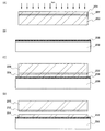
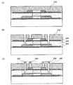
図1に、本発明の半導体装置の構成の一例を示す。図1(A)は本発明の半導体装置の平面図であり、図1(B)は図1(A)のA−Bにおける断面図であり、図1(C)は図1(A)のC−Dにおける断面図である。なお、図1の構成はあくまでも一例であり、本発明は該構成に限定されるものではない。 FIG. 1 shows an example of a structure of a semiconductor device of the present invention. 1A is a plan view of a semiconductor device of the present invention, FIG. 1B is a cross-sectional view taken along line AB of FIG. 1A, and FIG. 1C is a cross-sectional view of FIG. It is sectional drawing in CD. Note that the configuration in FIG. 1 is merely an example, and the present invention is not limited to this configuration.
図1に示す半導体装置は、2層の単結晶半導体層(単結晶半導体層100及び単結晶半導体層102)を有している。単結晶半導体層100は、絶縁層104、及び導電層106と共に第1のトランジスタ108を構成している。単結晶半導体層102は、導電層106及び絶縁層110と共に第2のトランジスタ112を構成している。ここで、第1のトランジスタ108はn型トランジスタであり、第2のトランジスタ112はp型トランジスタである。また、第1のトランジスタ108のソース領域又はドレイン領域の一部には、ソース電極又はドレイン電極114(以下、ソース配線又はドレイン配線とも言う)が電気的に接続されており、第2のトランジスタ112のソース領域又はドレイン領域の一部には、ソース電極又はドレイン電極116が電気的に接続されており、第1のトランジスタ及び第2のトランジスタのソース領域又はドレイン領域を電気的に接続するように、ソース電極又はドレイン電極118が設けられている。
The semiconductor device illustrated in FIG. 1 includes two single crystal semiconductor layers (a single
図1(D)は、上記半導体装置の回路図である。図1(D)からも分かるように、第1のトランジスタ108及び第2のトランジスタ112により、相補型回路(より詳細には、CMOSインバータ回路)が形成されている。導電層106は第1のトランジスタ108及び第2のトランジスタ112のゲート電極として機能し、CMOS回路の入力端子に当たる。また、ソース電極又はドレイン電極118は、CMOS回路の出力端子に当たる。
FIG. 1D is a circuit diagram of the semiconductor device. As can be seen from FIG. 1D, the
図1に示すように、単結晶半導体層を積層して半導体素子(例えば、トランジスタ)を形成することにより、高度に集積化した半導体装置を作製することができる。また、本発明では、全ての半導体素子を、単結晶半導体を用いて形成するから、アモルファス半導体や多結晶半導体を用いる場合と比較して、優れた特性の半導体装置を提供することができる。さらに、本発明においては、単結晶半導体層に電界を加えるための導電層(ゲート電極)を共通化することにより、トランジスタごとの導電層が不要となる。つまり、複数の導電層を積層して形成する必要がないため、低コストに半導体装置を作製することができる。図1の如き相補型回路(CMOS回路、相補型半導体装置とも言う)を形成する場合には、そのメリットは顕著である。 As shown in FIG. 1, a highly integrated semiconductor device can be manufactured by stacking single crystal semiconductor layers to form a semiconductor element (eg, a transistor). In the present invention, since all semiconductor elements are formed using a single crystal semiconductor, a semiconductor device having excellent characteristics can be provided as compared with the case where an amorphous semiconductor or a polycrystalline semiconductor is used. Further, in the present invention, by using a common conductive layer (gate electrode) for applying an electric field to the single crystal semiconductor layer, a conductive layer for each transistor becomes unnecessary. That is, since it is not necessary to stack a plurality of conductive layers, a semiconductor device can be manufactured at low cost. In the case of forming a complementary circuit (also referred to as a CMOS circuit or a complementary semiconductor device) as shown in FIG. 1, the merit is remarkable.
次に、本発明の半導体装置の製造方法の一例について図2乃至7を参照して以下に説明する。 Next, an example of a method for manufacturing a semiconductor device according to the present invention will be described below with reference to FIGS.
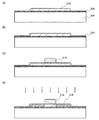
はじめに、単結晶半導体基板200を用意する。そして、単結晶半導体基板200の表面にイオンを照射し、単結晶半導体基板200中に損傷領域202及び単結晶半導体層204を形成する(図2(A)参照)。損傷領域202の形成方法としては、半導体層への不純物元素の添加に用いられる方法(イオンドーピング法)や、イオン化したガスを質量分離して選択的に半導体層に注入する方法(イオン注入法)等が挙げられる。イオンの照射は、形成される単結晶半導体層204の厚さを考慮して行えば良い。該単結晶半導体層204の厚さは5nm乃至500nm程度とすればよく、10nm乃至200nmの厚さとするとより好ましい。イオンを照射する際の加速電圧は上記の厚さを考慮して決定することができる。
First, a single
単結晶半導体基板200は、単結晶半導体からなる基板であれば特に限られないが、本実施の形態においては一例として、単結晶シリコン基板を用いることとする。その他、ゲルマニウム基板や、ガリウムヒ素、インジウムリンなどの化合物半導体による基板を適用することもできる。
Although the single
照射するイオンとしては、フッ素に代表されるハロゲンや、水素、ヘリウム等のイオンが挙げられる。ハロゲンのイオンとしてフッ素イオンを照射する場合には、原料ガスとしてBF3を用いれば良い。たとえば、単結晶半導体基板200として単結晶シリコン基板を用いて、該単結晶シリコン基板にフッ素イオンのようなハロゲンイオンを照射した場合には、損傷領域202には微小な空洞が形成される。これは、打ち込まれたハロゲンイオンがシリコン結晶格子内のシリコン原子を追い出すためと考えられる。このようにして形成された微小な空洞の体積を変化させることにより、単結晶シリコン基板を分離することができる。具体的には、低温の熱処理によって微小な空洞の体積変化を誘起する。なお、フッ素イオンを照射した後に、水素イオンを照射して空洞内に水素を含ませるようにしても良い。
Examples of ions to be irradiated include halogens represented by fluorine, ions of hydrogen, helium, and the like. In the case of irradiation with fluorine ions as halogen ions, BF 3 may be used as a source gas. For example, when a single crystal silicon substrate is used as the single
また、同一の原子から成り、質量の異なる複数のイオンを照射してもよい。例えば、水素を用いる場合には、H+、H2 +、H3 +イオンを含ませると共に、H3 +イオンの割合を高めておくと良い。H3 +イオンの割合を高めることで照射効率を高めることができるため、照射時間を短縮することができる。 Moreover, you may irradiate several ion which consists of the same atoms and from which mass differs. For example, when hydrogen is used, it is preferable to include H + , H 2 + , and H 3 + ions and to increase the ratio of H 3 + ions. Since the irradiation efficiency can be increased by increasing the ratio of H 3 + ions, the irradiation time can be shortened.
なお、損傷領域202の形成前に、単結晶半導体基板200の表面に保護層を形成する構成としても良い。保護層を形成することにより、イオンの照射に伴う単結晶半導体基板の表面の荒れを低減することができる。保護層としては、酸化シリコン、窒化シリコン、窒化酸化シリコン、酸化窒化シリコン等を用いることができる。
Note that a protective layer may be formed on the surface of the single
なお、酸化窒化シリコンとは、その組成において、窒素よりも酸素の含有量が多いものを示し、例えば、酸素が50原子%以上70原子%以下、窒素が0.5原子%以上15原子%以下、珪素が25原子%以上35原子%以下、水素が0.1原子%以上10原子%以下の範囲で含まれるものをいう。また、窒化酸化シリコンとは、その組成において、酸素よりも窒素の含有量が多いものを示し、例えば、酸素が5原子%以上30原子%以下、窒素が20原子%以上55原子%以下、珪素が25原子%以上35原子%以下、水素が10原子%以上25原子%以下の範囲で含まれるものをいう。但し、上記範囲は、ラザフォード後方散乱法(RBS:Rutherford Backscattering Spectrometry)や、水素前方散乱法(HFS:Hydrogen Forward Scattering)を用いて測定した場合のものである。また、構成元素の含有比率は、その合計が100原子%を超えない値をとる。 Note that silicon oxynitride indicates a composition whose oxygen content is higher than that of nitrogen. For example, oxygen is 50 atomic% to 70 atomic% and nitrogen is 0.5 atomic% to 15 atomic%. In this case, silicon is contained in the range of 25 atomic% to 35 atomic% and hydrogen in the range of 0.1 atomic% to 10 atomic%. Silicon nitride oxide refers to a composition having a nitrogen content higher than that of oxygen. For example, oxygen is 5 atomic% to 30 atomic%, nitrogen is 20 atomic% to 55 atomic%, silicon In the range of 25 atomic% to 35 atomic% and hydrogen in the range of 10 atomic% to 25 atomic%. However, the above ranges are those measured using Rutherford Backscattering Spectrometry (RBS) or Hydrogen Forward Scattering (HFS). Further, the content ratio of the constituent elements takes a value that the total does not exceed 100 atomic%.
次に、絶縁表面を有する基板206上に、接合層208を形成する(図2(B)参照)。接合層208は、酸化シリコン膜を、有機シランガスを用いた化学気相成長法(CVD法)により形成すると良い。その他に、シランガスを用いて化学気相成長法により作製される酸化シリコン膜を適用することもできる。なお、接合層208は絶縁性材料より形成されるため、絶縁層と呼ぶことができる。
Next, the
なお、絶縁表面を有する基板206としては、アルミノシリケートガラス、アルミノホウケイ酸ガラス、バリウムホウケイ酸ガラスのような電子工業用に使われる各種ガラス基板、石英基板、セラミック基板、サファイア基板等を用いることができる。好ましくはガラス基板を用いるのがよく、例えば第6世代(1500mm×1850mm)、第7世代(1870mm×2200mm)、第8世代(2200mm×2400mm)と呼ばれる大面積のマザーガラス基板を用いることもできる。大面積のマザーガラス基板を、絶縁表面を有する基板206として用いることで、半導体基板の大面積化が実現できる。なお、絶縁表面を有する基板206は上記の基板に限定されるものではない。例えば、耐熱温度が許せば樹脂材料からなる基板を用いることも可能である。もちろん、シリコンウエハのような単結晶半導体基板を用いても良い。この場合、単結晶半導体基板上に絶縁層を形成したものを用いれば良い。また、あらかじめ素子を形成した単結晶半導体基板上に絶縁層を形成したものを用いても良い。これにより、一層の集積化を図ることができる。
Note that as the
接合層208は平滑に形成され、親水性表面を有する。この接合層208としては酸化シリコン膜が適している。特に有機シランガスを用いて化学気相成長法により作製される酸化シリコン膜が好ましい。有機シランガスとしては、珪酸エチル(TEOS:Si(OC2H5)4)、トリメチルシラン((CH3)3SiH)、テトラメチルシラン((CH3)4Si)、テトラメチルシクロテトラシロキサン(TMCTS)、オクタメチルシクロテトラシロキサン(OMCTS)、ヘキサメチルジシラザン(HMDS)、トリエトキシシラン(SiH(OC2H5)3)、トリスジメチルアミノシラン(SiH(N(CH3)2)3)等のシリコン含有化合物を用いることができる。
The
上記接合層208は、5nm乃至500nm程度の厚さで設けられる。これにより、被成膜表面を平滑化すると共に当該膜の成長表面の平滑性を確保することが可能である。また、接合する基板との歪みを緩和することができる。なお、後の単結晶半導体基板200にも同様の接合層を設けておくことができる。このように、接合を形成する面の一方若しくは双方を、有機シランを原材料として成膜した酸化シリコン膜とすることで、接合を非常に強固なものとすることができる。
The
なお、絶縁表面を有する基板206と接合層208との間に、バリア層を設ける構成としてもよい。バリア層は窒化シリコン、窒化酸化シリコン又は酸化窒化シリコンから選ばれた一又は複数の材料を用いて形成すると良い。なお、バリア層は単層構造でも良いし積層構造でも良い。バリア層は、絶縁表面を有する基板206中の可動イオンや水分等の不純物が、接合層208、又は、接合層208より上に形成される層に侵入することを防ぐために設けられる。なお、不純物の侵入を防ぐことができるのであれば、上記材料以外を用いたバリア層を形成しても良い。また、不純物の侵入が大きな問題とならない場合には、バリア層を設けない構成としても良い。
Note that a barrier layer may be provided between the
本実施の形態においては、単結晶半導体基板200に損傷領域202を形成した後に、絶縁表面を有する基板206上に接合層208を形成する場合について説明したが、本発明はこれに限られない。本発明では、絶縁表面を有する基板206に単結晶半導体層204を形成することができればよいから、損傷領域202と接合層208の形成の順序は特に問われない。例えば、絶縁表面を有する基板206上に接合層208を形成した後に単結晶半導体基板200に損傷領域202を形成しても良い。接合層208の形成と損傷領域202の形成の順序は特に問われず、各々を独立したタイミングにて形成することができる。
In this embodiment, the case where the
次に、接合層208と、単結晶半導体層204とを密接させる(図2(C)参照)。接合層208と単結晶半導体層204とを密接させて圧力をかけることで、水素結合や共有結合による強固な接合を形成することが可能である。なお、接合層208を介して絶縁表面を有する基板206と単結晶半導体基板200とを貼り合わせた後には、加熱処理を行うことが好ましい。加熱処理を行うことで接合強度をより向上させることができる。なお、接合層208と単結晶半導体層204との間に下地層を形成する構成としても良い。下地層を形成することにより、単結晶半導体層204への可動イオン等の侵入を防ぐことができる。下地層は、上記バリア層と同様の材料を用いて作製することができるがこれに限られるものではない。例えば、単結晶半導体層204側から酸化窒化シリコン膜、窒化酸化シリコン膜を積層して下地層とすることができる。
Next, the
良好な接合を形成するために、接合が形成される表面を活性化しておいても良い。例えば、接合を形成する面に原子ビーム又はイオンビームを照射する。原子ビーム又はイオンビームを利用する場合には、アルゴン等の不活性ガス原子ビーム又は不活性ガスイオンビームを用いることができる。その他に、プラズマ処理又はラジカル処理を行う。このような表面処理により、200℃乃至400℃程度の低温で異種材料間の接合を形成することができる。 In order to form a good bond, the surface on which the bond is formed may be activated. For example, an atomic beam or an ion beam is irradiated to the surface on which the junction is formed. When an atomic beam or an ion beam is used, an inert gas atom beam such as argon or an inert gas ion beam can be used. In addition, plasma treatment or radical treatment is performed. By such surface treatment, a bond between different materials can be formed at a low temperature of about 200 ° C. to 400 ° C.
次に、加熱処理を行い、損傷領域202の一部を分離面として単結晶半導体層204を単結晶半導体基板200から分離する(図2(D)参照)。例えば、400℃乃至600℃の熱処理を行うことにより、損傷領域202に形成された微小な空洞の体積変化を誘起して分離させることができる。接合層208は絶縁表面を有する基板206と接合しているので、絶縁表面を有する基板206上には単結晶半導体層204が残存することとなる。なお、図2においては、損傷領域202と単結晶半導体層204との界面にて分離した様子を図示したが、本発明はこれに限られない。例えば、損傷領域202と単結晶半導体基板200との界面にて分離しても良いし、損傷領域202の一部にて分離しても良い。分離が生じる領域は、損傷領域202を形成する際の条件により異なるものと考えられる。
Next, heat treatment is performed so that the single
なお、絶縁表面を有する基板206としてガラス基板を用いる場合には、ガラス基板の歪み点近傍、具体的には歪み点±50℃で加熱を行えば良い。より具体的には、580℃以上680℃以下で行えばよい(ガラス基板の歪み点温度が630℃程度の場合)。なお、ガラス基板は加熱によって収縮するという性質を有する。このため、あらかじめガラス基板を歪み点近傍、具体的には歪み点±50℃程度(若しくはそれ以上)で加熱しておくと、その後の加熱処理における収縮を抑制することができる。これにより、熱膨張率の異なる単結晶半導体層を接合したガラス基板に加熱処理を行う場合であっても、ガラス基板からの単結晶半導体層の剥離を防ぐことができる。また、ガラス基板及び単結晶半導体層の反りなどの変形を防止することもできる。
Note that in the case where a glass substrate is used as the
なお、ガラス基板を用いる場合には、加熱終了時の急速な冷却を避けることが好ましい。具体的には2℃/分以下、好ましくは0.5℃/分以下、より好ましくは0.3℃/分以下の速度で、歪み点以下の温度まで冷却するとよい。降温速度を小さくすることにより、ガラス基板が縮む際に生じる局所的な応力を緩和することができる。該加熱処理は大気圧下で行っても良いし、減圧下で行っても良い。雰囲気も窒素雰囲気、酸素雰囲気など、適宜設定することができる。なお、該加熱処理は、加熱後に収縮する性質を有する基板を用いる場合であればガラス基板に限らず適用することができる。 In addition, when using a glass substrate, it is preferable to avoid rapid cooling at the end of heating. Specifically, it is good to cool to a temperature below the strain point at a rate of 2 ° C./min or less, preferably 0.5 ° C./min or less, more preferably 0.3 ° C./min or less. By reducing the temperature decrease rate, local stress generated when the glass substrate shrinks can be relaxed. The heat treatment may be performed under atmospheric pressure or under reduced pressure. The atmosphere can also be set as appropriate, such as a nitrogen atmosphere or an oxygen atmosphere. Note that the heat treatment is not limited to the glass substrate as long as a substrate having a property of shrinking after heating is used.
なお、接合の工程に係る加熱処理と、分離の工程に係る加熱処理とを同時に行うこともできる。この場合、1度の加熱処理で二つの工程を行うことができるため、低コストに半導体基板を作製することができる。 Note that the heat treatment related to the bonding step and the heat treatment related to the separation step can be performed simultaneously. In this case, since two steps can be performed by one heat treatment, a semiconductor substrate can be manufactured at low cost.
上記の工程によって得られた単結晶半導体層204については、化学的機械的研磨(Chemical Mechanical Polishing:CMP)、レーザー光の照射、ドライエッチング等により表面を平坦化することが好ましい。単結晶半導体層204の平坦性を向上することにより、後に形成する半導体素子のばらつきを抑えることができる。なお、所望の特性が得られるようであれば、CMPやレーザー光照射、ドライエッチング等は省略してもかまわない。レーザー光の照射を行う場合には、イオン照射に起因する欠陥を低減することもできる。
The single
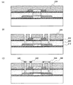
次に、単結晶半導体層204を所望の形状にパターニングして、島状の単結晶半導体層210を形成する(図3(A)参照)。パターニングの際のエッチング加工としては、プラズマエッチング(ドライエッチング)、ウエットエッチングのどちらを採用しても良いが、大面積基板を処理するにはプラズマエッチングが適している。エッチングガスとしては、CF4、NF3、Cl2、BCl3、などのフッ素系又は塩素系のガスを用い、HeやArなどの不活性ガスを適宜加えても良い。また、大気圧放電のエッチング加工を適用すれば、局所的な放電加工も可能であり、基板の全面にマスク層を形成する必要はない。
Next, the single
単結晶半導体層204をパターニングして、島状の単結晶半導体層210を形成した後には、しきい値電圧を制御するために、硼素、アルミニウム、ガリウムなどのp型不純物を添加すると良い。例えば、p型不純物として、硼素を1×1016cm−3以上1×1018cm−3以下の濃度で添加することができる。なお、適切な不純物濃度の単結晶半導体基板を用いることにより、しきい値電圧制御のためのドーピング工程は省略することができる。
After the single
次に、島状の単結晶半導体層210を覆う絶縁層212を形成する(図3(B)参照)。絶縁層212はゲート絶縁層として機能する。絶縁層212はスパッタリング法、CVD法などを用い、厚さを2nm以上150nm以下程度として珪素を含む絶縁膜で形成する。具体的には、窒化珪素、酸化珪素、酸化窒化珪素、窒化酸化珪素に代表される珪素の酸化物材料又は窒化物材料等の材料で形成すればよい。なお、絶縁層212は単層構造であっても良いし、積層構造としても良い。さらに、島状の単結晶半導体層210と絶縁層212との間に、膜厚1nm以上100nm以下、好ましくは1nm以上10nm以下、より好ましくは2nm以上5nm以下の薄い酸化珪素膜を形成してもよい。なお、低い温度でリーク電流の少ないゲート絶縁層を形成するために、アルゴンなどの希ガス元素を反応ガスに含ませても良い。
Next, an insulating
次に、絶縁層212上に導電層を形成し、該導電層をパターニングすることで導電層214を形成する(図3(C)参照)。導電層214はゲート電極として機能する。ここでは、単層構造にて導電層214を形成したが、本発明はこれに限られない。2層以上の積層構造としても良い。導電層214の厚さとしては、20nm以上500nm以下程度が好適である。なお、導電層214は、スパッタリング法、蒸着法、CVD法等の手法により形成することができる。用いることができる材料としては、タンタル(Ta)、タングステン(W)、チタン(Ti)、モリブデン(Mo)、アルミニウム(Al)、銅(Cu)、クロム(Cr)、ネオジム(Nd)から選ばれた元素、又は前記の元素を主成分とする合金材料もしくは化合物材料等が挙げられる。リン等の不純物元素をドーピングした多結晶シリコンに代表される半導体材料や、AgPdCu合金などを用いてもよい。
Next, a conductive layer is formed over the insulating
次に、導電層214をマスクとして、n型を付与する不純物元素を添加し、不純物領域216及びチャネル形成領域218を形成する(図3(D)参照)。本実施の形態では、不純物元素を含むドーピングガスとしてホスフィン(PH3)を用いてドーピングを行う。ここでは、不純物領域216に、n型を付与する不純物元素であるリン(P)が1×10¹⁹/cm3以上1×1021/cm3以下程度の濃度で含まれるようにする。
Next, an impurity element imparting n-type conductivity is added using the
なお、本実施の形態においては、島状の単結晶半導体層210にn型を付与する不純物元素を添加する構成としたが、本発明はこれに限られない。p型を付与する不純物元素を添加する構成としても良い。p型を付与する不純物元素を添加する場合には、不純物元素(例えば、ボロン(B))の濃度が1×10²⁰/cm3以上5×1021/cm3以下程度となるようにする。また、不純物領域216とチャネル形成領域218との間にLDD領域を形成する構成としても良い。LDD領域における不純物元素の濃度は1×1017/cm3以上1×1019/cm3以下程度とするのが好適である。
Note that although an impurity element imparting n-type conductivity is added to the island-shaped single
以上の工程により、第1のトランジスタを構成する島状の単結晶半導体層210、絶縁層212、導電層214が形成されたことになる。なお、不純物領域216の活性化のために加熱処理等を施しても良い。
Through the above steps, the island-shaped single
次に、絶縁層212及び導電層214を覆うように絶縁層220を形成する(図4(A)参照)。絶縁層212はスパッタリング法、蒸着法、CVD法、塗布法などを用いて形成することができる。絶縁層212に用いることができる材料としては、窒化珪素、酸化珪素、酸化窒化珪素、窒化酸化珪素に代表される珪素の酸化物材料又は窒化物材料等が挙げられる。また、酸化アルミニウム、窒化アルミニウム、酸化窒化アルミニウム、窒素含有量が酸素含有量よりも多い窒化酸化アルミニウム、ダイアモンドライクカーボン(DLC)、窒素含有炭素その他の無機絶縁性材料を含む物質から選ばれた材料を用いても良い。また、シロキサン樹脂を用いてもよい。なお、シロキサン樹脂とは、Si−O−Si結合を含む樹脂をいう。シロキサンは、シリコン(Si)と酸素(O)との結合で骨格構造が構成される。置換基として、少なくとも水素を含む有機基(例えばアルキル基、アリール基)が用いられる。有機基はフルオロ基を含んでいても良い。また、ポリイミド、アクリルポリマー、ポリアミド、ポリイミドアミド、ベンゾシクロブテン系材料、ポリシラザン等の有機絶縁性材料を用いることもできる。
Next, the insulating
絶縁層220の目的は、後に単結晶半導体層を接合する領域の平坦性を確保することにあるから、島状の単結晶半導体層210や絶縁層212、導電層214による凹凸が十分に小さい場合には、絶縁層220を形成しない構成としても構わない。しかしながら、凹凸がわずかに存在する場合であっても、接合の不良が生じる場合があるから、絶縁層220を設ける構成とすることが好ましい。
The purpose of the insulating
次に、絶縁層220の上面を、化学的機械的研磨(Chemical Mechanical Polishing:CMP)、レーザー光の照射、ドライエッチング等により平坦化する(図4(B)参照)。より具体的には、導電層214の表面が露出する程度に平坦化すると良い。これにより、後に単結晶半導体層を接合する際の不良を大きく低減することができる。ここで、絶縁層220の上面が十分に平坦である場合には、該平坦化の工程は省略しても構わない。なお、導電層214の表面が露出する程度に平坦化(研磨等)を行うことにより、後に形成される接合層のみをゲート絶縁層として用いることができることになる。接合層は非常に緻密な膜であり、十分に薄く形成することができるから、該接合層はゲート絶縁層として好適であり、該接合層を用いて形成したトランジスタは、その特性が非常に優れたものとなる。
Next, the upper surface of the insulating
次に、絶縁層220上に接合層222を形成する。また、単結晶半導体基板224の表面から所定の深さにイオンを打ち込むことにより、損傷領域226及び単結晶半導体層228を形成する。そして、接合層222と単結晶半導体層228を密接させる(図4(C)参照)。接合層222と単結晶半導体層228とを密接させて圧力をかけることで、水素結合や共有結合による強固な接合を形成することが可能である。なお、接合層222と単結晶半導体層228を密接させた後には、加熱処理を行うことが好ましい。加熱処理を行うことで接合強度をより向上させることができる。なお、接合層222と単結晶半導体層228との間に下地層を形成する構成としても良いが、接合層222のみをゲート絶縁層として用いたい場合には、下地層は形成しない。下地層を形成する場合には、窒化シリコン、窒化酸化シリコン又は酸化窒化シリコンから選ばれた一又は複数の材料を用いて形成すると良い。ここで、接合層222は絶縁性材料より形成されるため、絶縁層と呼ぶことができる。
Next, the
なお、絶縁層220上に接合層222を形成する工程と、単結晶半導体基板224に損傷領域226を形成する工程は、どちらを先に行っても良い。接合層222の形成と損傷領域226の形成の順序は特に問われず、各々を独立したタイミングにて形成することができる。接合に関する詳細については、上記の単結晶半導体層204と接合層208とを接合させる場合を参照できるため、ここでは省略する。
Note that either the step of forming the
次に、加熱処理を行い、損傷領域226の一部を分離面として単結晶半導体層228を単結晶半導体基板224から分離する(図5(A)参照)。例えば、400℃乃至600℃の熱処理を行うことにより、損傷領域226に形成された微小な空洞の体積変化を誘起して分離させることができる。これにより、絶縁層220上には単結晶半導体層228が残存することとなる。なお、図5においては、損傷領域226と単結晶半導体層228との界面にて分離した様子を図示したが、本発明はこれに限られない。例えば、損傷領域226と単結晶半導体基板224との界面にて分離しても良いし、損傷領域226の一部にて分離しても良い。分離が生じる領域は、損傷領域226を形成する際の条件により異なるものと考えられる。
Next, heat treatment is performed so that the single
なお、分離の際の加熱条件の詳細については、上記の単結晶半導体層204を形成する場合を参照できるため、ここでは省略する。以上の工程により、絶縁層220上に単結晶半導体層228を形成することができる(図5(B)参照)。
Note that the details of the heating conditions in the separation are omitted here because the case where the single
上記の工程によって得られた単結晶半導体層228については、化学的機械的研磨(Chemical Mechanical Polishing:CMP)、レーザー光の照射、ドライエッチング等により表面を平坦化することが好ましい。単結晶半導体層228の平坦性を向上することにより、後に形成する半導体素子のばらつきを抑えることができる。なお、所望の特性が得られるようであれば、CMPやレーザー光照射、ドライエッチング等は省略してもかまわない。レーザー光の照射を行う場合には、イオン注入に起因する欠陥を低減することもできる。
The single
次に、単結晶半導体層228を所望の形状にパターニングして、島状の単結晶半導体層230を形成する(図5(C)参照)。パターニングの際のエッチング加工としては、プラズマエッチング(ドライエッチング)、ウエットエッチングのどちらを採用しても良いが、大面積基板を処理するにはプラズマエッチングが適している。エッチングガスとしては、CF4、NF3、Cl2、BCl3、などのフッ素系又は塩素系のガスを用い、HeやArなどの不活性ガスを適宜加えても良い。また、大気圧放電のエッチング加工を適用すれば、局所的な放電加工も可能であり、基板の全面にマスク層を形成する必要はない。
Next, the single
本実施の形態においては、島状の単結晶半導体層230が、島状の単結晶半導体層210より小さくなるようにパターニングする。これは、後に配線(又は電極)を形成する際に、島状の単結晶半導体層210と配線とのコンタクトを良好に形成するためである。ただし、島状の単結晶半導体層210と配線とのコンタクトが適切に形成できるのであれば、これに限られない。
In this embodiment, patterning is performed so that the island-shaped single
単結晶半導体層228をパターニングして、島状の単結晶半導体層230を形成した後には、しきい値電圧を制御するために、硼素、アルミニウム、ガリウムなどのp型不純物を添加すると良い。例えば、p型不純物として、硼素を1×1016cm−3以上1×1018cm−3以下の濃度で添加することができる。なお、適切な不純物濃度の単結晶半導体基板を用いることにより、しきい値電圧制御のためのドーピング工程は省略することができる。
After the single
次に、フォトリソグラフィ法を用いて、島状の単結晶半導体層230上にレジスト材料からなるマスク232を形成する(図6(A)参照)。なお、マスク232は導電層214をマスクとして用いた裏面露光により自己整合的に形成しても良いし、メタルマスクを用いた上面からの露光により形成しても良い。裏面露光により自己整合的にマスク232を形成する場合には、単結晶半導体層や絶縁層を十分に透過する波長の光を用いることが好ましい。例えば、高圧水銀ランプのg線(波長:436nm)等を用いることができる。
Next, a
その後、マスク232を用いてp型を付与する不純物元素を添加し、不純物領域234及びチャネル形成領域236を形成する(図6(B)参照)。本実施の形態では、不純物元素を含むドーピングガスとしてジボラン(B2H6)を用いてドーピングを行う。ここでは、不純物領域234にボロン(B)が1×10²⁰/cm3以上5×1021/cm3以下程度の濃度で含まれるようにする。
After that, an impurity element imparting p-type conductivity is added using the
なお、本実施の形態においては、島状の単結晶半導体層230にp型を付与する不純物元素を添加する構成としたが、本発明はこれに限られない。n型を付与する不純物元素を添加する構成としても良い。また、不純物領域234とチャネル形成領域236との間にLDD領域を形成する構成としても良い。
Note that although an impurity element imparting p-type conductivity is added to the island-shaped single
その後、マスク232を除去する(図6(C)参照)。マスク232の除去後には、不純物領域234の活性化のための加熱処理等を施しても良い。以上により、第2のトランジスタを構成する島状の単結晶半導体層230、接合層222(絶縁層)、導電層214が形成されたことになる。
After that, the
次に、島状の単結晶半導体層230及び接合層222を覆うように絶縁層238を形成する(図7(A)参照)。絶縁層238はスパッタリング法、蒸着法、CVD法、塗布法などを用いて形成することができる。絶縁層238に用いることができる材料としては、窒化珪素、酸化珪素、酸化窒化珪素、窒化酸化珪素に代表される珪素の酸化物材料又は窒化物材料等が挙げられる。また、酸化アルミニウム、窒化アルミニウム、酸化窒化アルミニウム、窒素含有量が酸素含有量よりも多い窒化酸化アルミニウム、ダイアモンドライクカーボン(DLC)、窒素含有炭素その他の無機絶縁性材料を含む物質から選ばれた材料を用いても良い。また、シロキサン樹脂を用いてもよい。なお、シロキサン樹脂とは、Si−O−Si結合を含む樹脂をいう。シロキサンは、シリコン(Si)と酸素(O)との結合で骨格構造が構成される。置換基として、少なくとも水素を含む有機基(例えばアルキル基、アリール基)が用いられる。有機基はフルオロ基を含んでいても良い。また、ポリイミド、アクリルポリマー、ポリアミド、ポリイミドアミド、ベンゾシクロブテン系材料、ポリシラザン等の有機絶縁性材料を用いることもできる。
Next, an insulating
次に、レジスト材料からなるマスクを用いて絶縁層212、絶縁層220、接合層222、絶縁層238にコンタクトホール(開口部)を形成する(図7(B)参照)。エッチングは、用いる材料の選択比によって、一回で行う構成としても良いし、複数回にて行う構成としても良い。
Next, contact holes (openings) are formed in the insulating
その後、開口部を覆うように導電層を形成し、該導電層をエッチングする。これにより、ソース領域又はドレイン領域の一部とそれぞれ電気的に接続するソース電極又はドレイン電極240(ソース配線又はドレイン配線とも言う)、ソース電極又はドレイン電極242、ソース電極又はドレイン電極244を形成する(図7(C)参照)。ソース電極又はドレイン電極には、アルミニウム(Al)、タンタル(Ta)、チタン(Ti)、モリブデン(Mo)、タングステン(W)、ネオジム(Nd)、クロム(Cr)、ニッケル(Ni)、白金(Pt)、金(Au)、銀(Ag)、銅(Cu)、マグネシウム(Mg)、スカンジウム(Sc)、コバルト(Co)、ニッケル(Ni)、亜鉛(Zn)、ニオブ(Nb)、シリコン(Si)、リン(P)、ボロン(B)、ヒ素(As)、ガリウム(Ga)、インジウム(In)、錫(Sn)から選択された一若しくは複数の元素、又は前記元素を成分として含有する化合物や合金材料(例えば、インジウム錫酸化物(ITO)、インジウム亜鉛酸化物(IZO)、酸化珪素を添加したインジウム錫酸化物(ITSO)、酸化亜鉛(ZnO)、アルミネオジム(Al−Nd)、マグネシウム銀(Mg−Ag)など)、若しくはこれらの化合物を組み合わせた物質等が用いられる。その他にも、シリサイド(例えば、アルミシリコン、モリブデンシリコン、ニッケルシリサイド)や、窒素を含有する化合物(例えば、窒化チタン、窒化タンタル、窒化モリブデン)、リン(P)等の不純物元素をドーピングしたシリコン(Si)等を用いることもできる。
After that, a conductive layer is formed so as to cover the opening, and the conductive layer is etched. Thus, a source or drain electrode 240 (also referred to as a source wiring or a drain wiring), a source or
以上の工程で、第1のトランジスタ及び第2のトランジスタからなる相補型回路246(CMOS回路)が形成された(図7(C)参照)。なお、本実施の形態においては、第1のトランジスタをn型とし、第2のトランジスタをp型としたが本発明はこれに限られない。第1のトランジスタをp型とし、第2のトランジスタをn型としても良い。また、異なる極性の二つのトランジスタを用いて相補型回路246を形成することに限られない。同じ極性のトランジスタを積層して形成しても良い。第1のトランジスタ及び第2のトランジスタを同じ極性とする場合には、ゲート電極として機能する導電層を独立して設けても良いし、共通化しても良い。例えば、第1のトランジスタと第2のトランジスタのチャネル形成領域への不純物元素の注入量を異ならせることで、ゲート電極を共通化した場合でも二つのトランジスタを独立させて動作させることが可能である。
Through the above steps, a complementary circuit 246 (CMOS circuit) including the first transistor and the second transistor was formed (see FIG. 7C). Note that in this embodiment mode, the first transistor is an n-type transistor and the second transistor is a p-type transistor, but the present invention is not limited to this. The first transistor may be a p-type and the second transistor may be an n-type. In addition, the
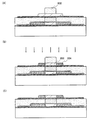
なお、本実施の形態においては、チャネル長方向に対して第1のトランジスタを形成する島状の単結晶半導体層210と、第2のトランジスタを形成する島状の単結晶半導体層230との大きさを異ならせる構成としたが、例えば、図19に示す構成のように、島状の単結晶半導体層210と島状の単結晶半導体層230とのチャネル幅方向の大きさを異ならせることも可能である。ここで、図19(A)は平面図であり、図19(B)は、図19(A)のE−Fにおける断面図である。図19において、ソース電極又はドレイン電極240(ソース配線又はドレイン配線とも言う)、ソース電極又はドレイン電極242、ソース電極又はドレイン電極244の対応関係は図7と同様であり、ソース電極又はドレイン電極244によって、二つのトランジスタが電気的に接続されている。また、図7と同様にゲート電極として機能する導電層214が設けられている。なお、ゲート電極として機能する導電層214はCMOS回路の入力端子に当たり、ソース電極又はドレイン電極244はCMOS回路の出力端子に当たる。図19から分かるように、第1の(下層の)トランジスタのチャネル幅(W1)は第2の(上層の)トランジスタのチャネル幅(W2)より大きくなっている。
Note that in this embodiment, the island-shaped single
上記のように相補型回路を形成する場合には、第1のトランジスタをp型とし、第2のトランジスタをn型とすることで、二つのトランジスタの移動度の差を補完することができる。つまり、移動度の低いp型トランジスタのチャネル幅を、移動度の高いn型トランジスタのチャネル幅より大きくすることで、相対的にp型トランジスタを流れる電流を増加させることができる。すなわち、レイアウトの効率化と共に、相補型回路の動作の高速化を実現することができる。もちろん、上記構成に限らず、要求される電流等に応じて、第1のトランジスタと、第2のトランジスタのチャネル幅を適宜変更しても良い。 In the case where a complementary circuit is formed as described above, the difference in mobility between two transistors can be complemented by making the first transistor p-type and the second transistor n-type. That is, the current flowing through the p-type transistor can be relatively increased by making the channel width of the p-type transistor with low mobility larger than the channel width of the n-type transistor with high mobility. That is, it is possible to increase the speed of the operation of the complementary circuit along with the efficiency of the layout. Needless to say, the channel widths of the first transistor and the second transistor may be changed as appropriate in accordance with a required current or the like without being limited to the above structure.
本発明の如く、単結晶半導体層を積層して半導体素子(例えば、トランジスタ)を形成することにより、プロセスルールの微細化に頼らずに、高度に集積化した半導体装置を作製することができる。つまり、小型かつ高性能な半導体装置を提供することができる。また、プロセスルールの微細化に起因する様々な問題点を解消することができる。また、すべての半導体素子を単結晶半導体を用いて形成するため、アモルファス半導体や多結晶半導体を用いる場合と比較して、優れた特性の半導体装置を提供することができる。 By stacking single crystal semiconductor layers to form a semiconductor element (eg, a transistor) as in the present invention, a highly integrated semiconductor device can be manufactured without depending on miniaturization of process rules. That is, a small and high-performance semiconductor device can be provided. In addition, various problems caused by miniaturization of process rules can be solved. In addition, since all semiconductor elements are formed using a single crystal semiconductor, it is possible to provide a semiconductor device with superior characteristics as compared with the case where an amorphous semiconductor or a polycrystalline semiconductor is used.
また、本発明においては、単結晶半導体層に電界を加える導電層(いわゆるゲート電極)を共通化する。これにより、複数の導電層を形成する必要がないため、低コストに半導体装置を作製することができる。特に、相補型回路(CMOS回路、相補型半導体装置とも言う)を形成する場合には、そのメリットは顕著である。例えば2層の単結晶半導体層にて形成されるすべての回路を相補型回路とした場合には、従来の如く1層の半導体層により相補型回路を形成する場合と比較して、実に2倍の集積度を実現することができる。しかも、ゲート電極はその大部分が共通化されるため、非常に低コストである。さらに、配線が共通化されるため、回路全体の配線長を短縮することができる。すなわち、配線容量に起因する消費電力を低減することができ、低消費電力化に大きく貢献する。 In the present invention, a conductive layer (so-called gate electrode) for applying an electric field to the single crystal semiconductor layer is shared. Accordingly, it is not necessary to form a plurality of conductive layers, so that a semiconductor device can be manufactured at low cost. In particular, when a complementary circuit (also referred to as a CMOS circuit or a complementary semiconductor device) is formed, the merit is remarkable. For example, when all the circuits formed of two single crystal semiconductor layers are complementary circuits, the circuit is doubled compared to the case of forming a complementary circuit with one semiconductor layer as in the prior art. The degree of integration can be realized. In addition, since most of the gate electrode is shared, the cost is very low. Furthermore, since the wiring is shared, the wiring length of the entire circuit can be shortened. That is, the power consumption due to the wiring capacity can be reduced, which greatly contributes to a reduction in power consumption.
もちろん、3層以上の多層構造とすることにより、さらなる集積化を容易に実現することができる。この場合にも、本実施の形態にて説明した作製方法を参照して多層半導体構造を実現することができる。 Of course, further integration can be easily realized by using a multilayer structure of three or more layers. Also in this case, a multilayer semiconductor structure can be realized with reference to the manufacturing method described in this embodiment mode.
(実施の形態2)
本実施の形態では、本発明の半導体装置の製造方法の別の一例について、図8乃至13を参照して説明する。なお、本実施の形態において、実施の形態1を参照できる部分については詳細な説明を省略することとする。
(Embodiment 2)
In this embodiment mode, another example of a method for manufacturing a semiconductor device of the present invention will be described with reference to FIGS. Note that in this embodiment, detailed description of portions to which
はじめに、単結晶半導体基板800を用意する。そして、単結晶半導体基板800の表面から所定の深さにイオンを打ち込み、損傷領域802及び単結晶半導体層804を形成する(図8(A)参照)。損傷領域802及び単結晶半導体層804の形成方法の詳細については、実施の形態1を参照できるため、ここでは省略する。
First, a single
単結晶半導体基板800は、単結晶半導体材料からなる基板であれば特に限られないが、本実施の形態においては一例として、単結晶シリコン基板を用いることとする。その他、ゲルマニウム基板や、ガリウムヒ素、インジウムリンなどの化合物半導体による基板を適用することもできる。
Although the single
なお、損傷領域802の形成前に、単結晶半導体基板800の表面に保護層を形成する構成としても良い。保護層を形成することにより、イオンの照射に伴う単結晶半導体基板の表面の荒れを低減することができる。保護層としては、酸化シリコン、窒化シリコン、窒化酸化シリコン、酸化窒化シリコン等を用いることができる。
Note that a protective layer may be formed on the surface of the single
次に、単結晶半導体層804上に、接合層806を形成する(図8(B)参照)。接合層806は、酸化シリコン膜を、有機シランガスを用いた化学気相成長法(CVD法)により形成すると良い。その他に、シランガスを用いて化学気相成長法により作製される酸化シリコン膜を適用することもできる。なお、接合層806は絶縁性材料より形成されるため、絶縁層と呼ぶことができる。接合層806の詳細については、実施の形態1を参照できるため、ここでは省略する。
Next, the
なお、単結晶半導体層804と接合層806との間に、下地層を設ける構成としてもよい。下地層は窒化シリコン、窒化酸化シリコン若しくは酸化窒化シリコンから選ばれた一又は複数の材料を用いて形成すると良い。なお、下地層は単層構造でも良いし積層構造でも良い。下地層は、可動イオンや水分等の不純物が、単結晶半導体層804に侵入することを防ぐために設けられる。なお、不純物の侵入を防ぐことができるのであれば、上記材料以外を用いた下地層を形成しても良い。また、不純物の侵入が大きな問題とならない場合には、下地層を設けない構成としても良い。上記にて保護層を形成した場合には、該保護層を下地層として用いても良い。
Note that a base layer may be provided between the single
次に、絶縁表面を有する基板808と、接合層806とを密接させる(図8(C)参照)。絶縁表面を有する基板808と接合層806とを密接させて圧力をかけることで、水素結合や共有結合による強固な接合を形成することが可能である。なお、接合層806を介して絶縁表面を有する基板808と単結晶半導体基板800とを貼り合わせた後には、加熱処理を行うことが好ましい。加熱処理を行うことで接合強度をより向上させることができる。また、接合層806と絶縁表面を有する基板808との間にバリア層を形成する構成としても良い。バリア層を形成することにより、単結晶半導体層804への可動イオン等の侵入を防ぐことができる。バリア層は、上記下地層と同様の材料を用いて作製することができるがこれに限られるものではない。
Next, the
なお、絶縁表面を有する基板808としては、アルミノシリケートガラス、アルミノホウケイ酸ガラス、バリウムホウケイ酸ガラスのような電子工業用に使われる各種ガラス基板、石英基板、セラミック基板、サファイア基板等を用いることができる。好ましくはガラス基板を用いるのがよく、例えば第6世代(1500mm×1850mm)、第7世代(1870mm×2200mm)、第8世代(2200mm×2400mm)と呼ばれる大面積のマザーガラス基板を用いることもできる。大面積のマザーガラス基板を、絶縁表面を有する基板808として用いることで、半導体基板の大面積化が実現できる。なお、絶縁表面を有する基板808は上記の基板に限定されるものではない。例えば、耐熱温度が許せば樹脂材料からなる基板を用いることも可能である。
Note that as the
良好な接合を形成するために、接合が形成される表面を活性化しておいても良い。例えば、接合を形成する面に原子ビーム若しくはイオンビームを照射する。原子ビーム又はイオンビームを利用する場合には、アルゴン等の不活性ガス原子ビーム又は不活性ガスイオンビームを用いることができる。その他に、プラズマ処理又はラジカル処理を行う。このような表面処理により、200℃乃至400℃程度の低温で異種材料間の接合を形成することができる。 In order to form a good bond, the surface on which the bond is formed may be activated. For example, an atomic beam or an ion beam is irradiated to the surface on which the junction is formed. When an atomic beam or an ion beam is used, an inert gas atom beam such as argon or an inert gas ion beam can be used. In addition, plasma treatment or radical treatment is performed. By such surface treatment, a bond between different materials can be formed at a low temperature of about 200 ° C. to 400 ° C.
次に、加熱処理を行い、損傷領域802の一部を分離面として単結晶半導体層804を単結晶半導体基板800から分離する(図8(D)参照)。例えば、400℃乃至600℃の熱処理を行うことにより、損傷領域802に形成された微小な空洞の体積変化を誘起して分離させることができる。接合層806は絶縁表面を有する基板808と接合しているので、絶縁表面を有する基板808上には単結晶半導体層804が残存することとなる。なお、図8においては、損傷領域802と単結晶半導体層804との界面にて分離した様子を図示したが、本発明はこれに限られない。例えば、損傷領域802と単結晶半導体基板800との界面にて分離しても良いし、損傷領域802の一部にて分離しても良い。分離が生じる領域は、損傷領域802を形成する際の条件により異なるものと考えられる。
Next, heat treatment is performed so that the single
その他の条件に関しては、実施の形態1を参照できるため、ここでは省略するものとする。 Regarding other conditions, the first embodiment can be referred to, and therefore omitted here.
次に、単結晶半導体層804を所望の形状にパターニングして、島状の単結晶半導体層810を形成する(図9(A)参照)。パターニングの際のエッチング加工としては、プラズマエッチング(ドライエッチング)、ウエットエッチングのどちらを採用しても良いが、大面積基板を処理するにはプラズマエッチングが適している。エッチングガスとしては、CF4、NF3、Cl2、BCl3、などのフッ素系又は塩素系のガスを用い、HeやArなどの不活性ガスを適宜加えても良い。また、大気圧放電のエッチング加工を適用すれば、局所的な放電加工も可能であり、基板の全面にマスク層を形成する必要はない。
Next, the single
単結晶半導体層804をパターニングして、島状の単結晶半導体層810を形成した後には、しきい値電圧を制御するために、硼素、アルミニウム、ガリウムなどのp型不純物を添加すると良い。例えば、p型不純物として、硼素を1×1016cm−3以上1×1018cm−3以下の濃度で添加することができる。なお、適切な不純物濃度の単結晶半導体基板を用いることにより、しきい値電圧制御のためのドーピング工程は省略することができる。
After the single
次に、島状の単結晶半導体層810を覆う絶縁層812を形成する(図9(B)参照)。絶縁層812はゲート絶縁層として機能する。絶縁層812はスパッタリング法、CVD法などを用い、厚さを2nm以上150nm以下程度として珪素を含む絶縁膜で形成する。詳細については、実施の形態1を参照することができる。
Next, an insulating
次に、絶縁層812上に導電層を形成し、該導電層をパターニングすることで導電層814を形成する(図9(C)参照)。導電層814はゲート電極として機能する。詳細については、実施の形態1を参照することができる。
Next, a conductive layer is formed over the insulating
次に、導電層814をマスクとして、n型を付与する不純物元素を添加し、不純物領域816及びチャネル形成領域818を形成する(図9(D)参照)。本実施の形態では、不純物元素を含むドーピングガスとしてホスフィン(PH3)を用いてドーピングを行う。ここでは、不純物領域816に、n型を付与する不純物元素であるリン(P)が1×10¹⁹/cm3以上1×1021/cm3以下程度の濃度で含まれるようにする。
Next, an impurity element imparting n-type conductivity is added using the
なお、本実施の形態においては、島状の単結晶半導体層810にn型を付与する不純物元素を添加する構成としたが、本発明はこれに限られない。p型を付与する不純物元素を添加する構成としても良い。p型を付与する不純物元素を添加する場合には、不純物元素(例えば、ボロン(B))の濃度が1×10²⁰/cm3以上5×1021/cm3以下程度となるようにする。また、不純物領域816とチャネル形成領域818との間にLDD領域を形成する構成としても良い。LDD領域における不純物元素の濃度は1×1017/cm3以上1×1019/cm3以下程度とするのが好適である。
Note that although an impurity element imparting n-type conductivity is added to the island-shaped single
以上の工程により、第1のトランジスタを構成する島状の単結晶半導体層810、絶縁層812、導電層814が形成されたことになる。なお、不純物領域816の活性化のために加熱処理等を施しても良い。
Through the above steps, the island-shaped single
次に、絶縁層812及び導電層814を覆うように絶縁層820を形成する(図10(A)参照)。絶縁層812はスパッタリング法、蒸着法、CVD法、塗布法などを用いて形成することができる。詳細については、実施の形態1を参照すればよい。
Next, an insulating
絶縁層820の目的は、後に単結晶半導体層を接合する領域の平坦性を確保することにあるから、島状の単結晶半導体層810や絶縁層812、導電層814による凹凸が十分に小さい場合には、絶縁層820を形成しない構成としても構わない。しかしながら、凹凸がわずかに存在する場合であっても、接合の不良が生じる場合があるから、絶縁層820を設ける構成とすることが好ましい。
The purpose of the insulating
次に、絶縁層820の上面を、化学的機械的研磨(Chemical Mechanical Polishing:CMP)、レーザー光の照射、ドライエッチング等により平坦化する(図10(B)参照)。より具体的には、導電層814の表面が露出する程度に平坦化すると良い。これにより、後に単結晶半導体層を接合する際の不良を大きく低減することができる。ここで、絶縁層820の上面が十分に平坦である場合には、該平坦化の工程は省略しても構わない。なお、導電層814の表面が露出する程度に平坦化(研磨等)を行うことにより、後に形成される接合層のみをゲート絶縁層として用いることができることになる。接合層は非常に緻密な膜であり、十分に薄く形成することができるから、該接合層はゲート絶縁層として好適であり、該接合層を用いて形成したトランジスタは、その特性が非常に優れたものとなる。
Next, the upper surface of the insulating
次に、単結晶半導体基板822の表面から所定の深さにイオンを打ち込むことにより、損傷領域824及び単結晶半導体層826を形成し、単結晶半導体層826上に接合層828を形成する。そして、接合層828と絶縁層820(及び導電層814)を密接させる(図10(C)参照)。接合層828と絶縁層820とを密接させて圧力をかけることで、水素結合や共有結合による強固な接合を形成することが可能である。なお、接合層828と絶縁層820を密接させた後には、加熱処理を行うことが好ましい。加熱処理を行うことで接合強度をより向上させることができる。なお、単結晶半導体層826と接合層828との間に下地層を形成する構成としても良いが、接合層828のみをゲート絶縁層として用いたい場合には、下地層は形成しない。下地層を形成する場合には、窒化シリコン、窒化酸化シリコン若しくは酸化窒化シリコンから選ばれた一又は複数の材料を用いて形成すると良い。ここで、接合層828は絶縁性材料より形成されるため、絶縁層と呼ぶことができる。
Next, ions are implanted to a predetermined depth from the surface of the single
次に、加熱処理を行い、損傷領域824の一部を分離面として単結晶半導体層826を単結晶半導体基板822から分離する(図11(A)参照)。例えば、400℃乃至600℃の熱処理を行うことにより、損傷領域824に形成された微小な空洞の体積変化を誘起して分離させることができる。これにより、絶縁層820上には単結晶半導体層826が残存することとなる。なお、図11においては、損傷領域824と単結晶半導体層826との界面にて分離した様子を図示したが、本発明はこれに限られない。例えば、損傷領域824と単結晶半導体基板822との界面にて分離しても良いし、損傷領域824の一部にて分離しても良い。分離が生じる領域は、損傷領域824を形成する際の条件により異なるものと考えられる。
Next, heat treatment is performed so that the single
なお、詳細な条件等については、実施の形態1等を参照できるため、ここでは省略する。以上の工程により、絶縁層820上に単結晶半導体層826を形成することができる(図11(B)参照)。
Note that detailed conditions and the like are omitted here because
次に、単結晶半導体層826を所望の形状にパターニングして、島状の単結晶半導体層830を形成する(図11(C)参照)。詳細については、実施の形態1を参照すればよい。
Next, the single
単結晶半導体層826をパターニングして、島状の単結晶半導体層830を形成した後には、しきい値電圧を制御するために、硼素、アルミニウム、ガリウムなどのp型不純物を添加すると良い。例えば、p型不純物として、硼素を1×1016cm−3以上1×1018cm−3以下の濃度で添加することができる。なお、適切な不純物濃度の単結晶半導体基板を用いることにより、しきい値電圧制御のためのドーピング工程は省略することができる。
After the single
次に、フォトリソグラフィ法を用いて、島状の単結晶半導体層830上にレジスト材料からなるマスク832を形成する(図12(A)参照)。そして、マスク832を用いて、p型を付与する不純物元素を添加し、不純物領域834及びチャネル形成領域836を形成する(図12(B)参照)。本実施の形態では、不純物元素を含むドーピングガスとしてジボラン(B2H6)を用いてドーピングを行う。ここでは、不純物領域834にボロン(B)が1×10²⁰/cm3以上5×1021/cm3以下程度の濃度で含まれるようにする。
Next, a
なお、本実施の形態においては、島状の単結晶半導体層830にp型を付与する不純物元素を添加する構成としたが、本発明はこれに限られない。n型を付与する不純物元素を添加する構成としても良い。また、不純物領域834とチャネル形成領域836との間にLDD領域を形成する構成としても良い。
Note that although an impurity element imparting p-type conductivity is added to the island-shaped single
その後、マスク832を除去する(図12(C)参照)。マスク832の除去後には、不純物領域834の活性化のための加熱処理等を施しても良い。以上により、第2のトランジスタを構成する島状の単結晶半導体層830、接合層828(絶縁層)、導電層814が形成されたことになる。
After that, the
次に、島状の単結晶半導体層830及び接合層828を覆うように絶縁層838を形成する(図13(A)参照)。詳細については、実施の形態1を参照することができる。
Next, an insulating
次に、レジスト材料からなるマスクを用いて絶縁層812、絶縁層820、接合層828、絶縁層838にコンタクトホール(開口部)を形成する(図13(B)参照)。エッチングは、用いる材料の選択比によって、一回で行う構成としても良いし、複数回にて行う構成としても良い。
Next, contact holes (openings) are formed in the insulating
その後、開口部を覆うように導電層を形成し、該導電層をエッチングする。これにより、ソース領域又はドレイン領域の一部とそれぞれ電気的に接続するソース電極又はドレイン電極840(ソース配線又はドレイン配線とも言う)、ソース電極又はドレイン電極842、ソース電極又はドレイン電極844を形成する(図13(C)参照)。詳細については、実施の形態1を参照することができる。
After that, a conductive layer is formed so as to cover the opening, and the conductive layer is etched. Thus, a source or drain electrode 840 (also referred to as a source wiring or a drain wiring), a source or
以上の工程で、第1のトランジスタ及び第2のトランジスタからなる相補型回路846(CMOS回路)が形成された(図13(C)参照)。なお、本実施の形態においては、第1のトランジスタをn型とし、第2のトランジスタをp型としたが本発明はこれに限られない。第1のトランジスタをp型とし、第2のトランジスタをn型としても良い。また、異なる極性の二つのトランジスタを用いて相補型回路846を形成することに限られない。同じ極性のトランジスタを積層して形成しても良い。
Through the above steps, a complementary circuit 846 (CMOS circuit) including the first transistor and the second transistor was formed (see FIG. 13C). Note that in this embodiment mode, the first transistor is an n-type transistor and the second transistor is a p-type transistor, but the present invention is not limited to this. The first transistor may be a p-type and the second transistor may be an n-type. In addition, the
また、本実施の形態においては、実施の形態1とは異なり、単結晶半導体基板側に接合層を設ける構成としたが、本発明はこれに限られない。実施の形態1の如く絶縁表面を有する基板側に接合層を設ける構成としても良い。また、第1のトランジスタの単結晶半導体層を形成する際の接合層は絶縁表面を有する基板側に形成し、第2のトランジスタの単結晶半導体層を形成する際の接合層は単結晶半導体基板側に形成する構成としても良い。もちろん、第1のトランジスタの単結晶半導体層を形成する際の接合層は単結晶半導体基板側に形成し、第2のトランジスタの単結晶半導体層を形成する際の接合層は絶縁表面を有する基板側に形成する構成としても良い。
In this embodiment mode, unlike the first embodiment mode, a bonding layer is provided on the single crystal semiconductor substrate side; however, the present invention is not limited to this. As in
本発明の如く、単結晶半導体層を積層して半導体素子(例えば、トランジスタ)を形成することにより、プロセスルールの微細化に頼らずに、高度に集積化した半導体装置を作製することができる。つまり、プロセスルールの微細化に起因する様々な問題点を解消することができる。また、すべての半導体素子を単結晶半導体を用いて形成するため、アモルファス半導体や多結晶半導体を用いる場合と比較して、優れた特性の半導体装置を提供することができる。 By stacking single crystal semiconductor layers to form a semiconductor element (eg, a transistor) as in the present invention, a highly integrated semiconductor device can be manufactured without depending on miniaturization of process rules. That is, various problems resulting from the refinement of process rules can be solved. In addition, since all semiconductor elements are formed using a single crystal semiconductor, it is possible to provide a semiconductor device with superior characteristics as compared with the case where an amorphous semiconductor or a polycrystalline semiconductor is used.
また、本発明においては、単結晶半導体層に電界を加える導電層(いわゆるゲート電極)を共通化する。これにより、複数の導電層を形成する必要がないため、低コストに半導体装置を作製することができる。特に、相補型回路(CMOS回路、相補型半導体装置とも言う)を形成する場合には、そのメリットは顕著である。例えば2層の単結晶半導体層にて形成されるすべての回路を相補型回路とした場合には、従来の如く1層の半導体層により相補型回路を形成する場合と比較して、実に2倍の集積度を実現することができる。しかも、ゲート電極はその大部分が共通化されるため、非常に低コストである。 In the present invention, a conductive layer (so-called gate electrode) for applying an electric field to the single crystal semiconductor layer is shared. Accordingly, it is not necessary to form a plurality of conductive layers, so that a semiconductor device can be manufactured at low cost. In particular, when a complementary circuit (also referred to as a CMOS circuit or a complementary semiconductor device) is formed, the merit is remarkable. For example, when all the circuits formed of two single crystal semiconductor layers are complementary circuits, the circuit is doubled compared to the case of forming a complementary circuit with one semiconductor layer as in the prior art. The degree of integration can be realized. In addition, since most of the gate electrode is shared, the cost is very low.
もちろん、3層以上の多層構造とすることにより、さらなる集積化を容易に実現することができる。この場合にも、本実施の形態にて説明した作製方法を参照してさらなる多層構造を実現することができる。 Of course, further integration can be easily realized by using a multilayer structure of three or more layers. Also in this case, a further multilayer structure can be realized with reference to the manufacturing method described in this embodiment mode.
本実施の形態は、実施の形態1と適宜組み合わせて用いることができる。
This embodiment can be combined with
(実施の形態3)
本実施の形態では、本発明の半導体装置の一例を、図14を参照して説明する。なお、本実施の形態においては、半導体装置の一例として液晶表示装置を挙げて説明するが、本発明により作製できる半導体装置は液晶表示装置に限られるものではない。
(Embodiment 3)
In this embodiment, an example of a semiconductor device of the present invention will be described with reference to FIGS. Note that although a liquid crystal display device is described as an example of a semiconductor device in this embodiment, a semiconductor device that can be manufactured according to the present invention is not limited to a liquid crystal display device.
図14に、本発明の液晶表示装置の一例を示す。図14(A)は液晶表示装置の平面図であり、図14(B)は図14(A)のE−Fにおける断面図である。該液晶表示装置は、実施の形態1や実施の形態2などに示した方法を用いて絶縁表面を有する基板1400上にトランジスタを形成した後、層間絶縁層1402、画素電極1404、スペーサ1406、配向膜として機能する絶縁層1408等を形成し、配向膜として機能する絶縁層1410、対向電極として機能する導電層1412、カラーフィルターとして機能する着色層1414、偏光子1416(偏光板ともいう)等が設けられた対向基板1420を貼り合わせ、空隙に液晶層1418を設けることで作製することができる。なお、絶縁表面を有する基板1400にも偏光子1422(偏光板)を設けるが、本発明はこれに限られない。例えば、反射型の液晶表示装置においては、偏光子は、一方に設ければ良い。
FIG. 14 shows an example of the liquid crystal display device of the present invention. 14A is a plan view of the liquid crystal display device, and FIG. 14B is a cross-sectional view taken along line EF in FIG. 14A. In the liquid crystal display device, after a transistor is formed over a
上記において、画素電極1404は、インジウム錫酸化物(ITO)、酸化インジウムに酸化亜鉛(ZnO)を混合したIZO(indium zinc oxide)、酸化インジウムに酸化珪素(SiO2)を混合した導電性材料、有機インジウム、有機スズ、酸化タングステンを含むインジウム酸化物、酸化タングステンを含むインジウム亜鉛酸化物、酸化チタンを含むインジウム酸化物、酸化チタンを含むインジウム錫酸化物、又はタングステン(W)、モリブデン(Mo)、ジルコニウム(Zr)、ハフニウム(Hf)、バナジウム(V)、ニオブ(Nb)、タンタル(Ta)、クロム(Cr)、コバルト(Co)、ニッケル(Ni)、チタン(Ti)、白金(Pt)、アルミニウム(Al)、銅(Cu)、銀(Ag)等の金属又はその合金、若しくはその金属窒化物を用いて形成することができる。また、導電性高分子(導電性ポリマーともいう)を含む導電性組成物を用いることもできる。導電性組成物は、薄膜におけるシート抵抗が10000Ω/sq.以下であることが好ましい。また、光透過性を有する画素電極層として薄膜を形成する場合には、波長550nmにおける透光率が70%以上であることが好ましい。また、含まれる導電性高分子の抵抗率が0.1Ω・cm以下であることが好ましい。
In the above, the
配向膜として機能する絶縁層1408や、配向膜として機能する絶縁層1410には、ラビング処理が施されている。これにより、液晶分子の配向を制御することができる。
The insulating
本実施の形態にて示した液晶表示装置は、外部端子接続領域1450、封止領域1452、駆動回路領域1454、及び画素領域1456より構成されている。
The liquid crystal display device described in this embodiment includes an external
外部端子接続領域1450では、画素領域1456と電気的に接続された端子電極層1424に、異方性導電体層1426を介してFPC1428が接続されている。FPC1428は、外部からの信号を伝達する役目を担う。封止領域1452ではシール材1430を用いて絶縁表面を有する基板1400と対向基板1420との封止が行われている。駆動回路領域1454にはnチャネル型トランジスタとpチャネル型トランジスタからなるCMOS回路1432が設けられている。また、画素領域1456にはnチャネル型トランジスタ1434、及び容量配線1436が形成されている。なお、画素領域1456におけるnチャネル型トランジスタ1434は、CMOS回路1432のnチャネル型トランジスタ(第1のトランジスタ)と同様にして作製することができる。また、容量配線1436は、各トランジスタにおいてゲート電極として機能する導電層と同じ層にて形成される。
In the external
本実施の形態においては、画素領域1456のトランジスタとして、nチャネル型トランジスタを用いる構成としているが、これに限られず、pチャネル型トランジスタを用いる構成としても良い。pチャネル型トランジスタを用いる場合には、CMOS回路1432のpチャネル型トランジスタ(第2のトランジスタ)と同様にして作製することができる。
In this embodiment mode, an n-channel transistor is used as the transistor in the
なお、画素領域1456に形成されるトランジスタを単結晶半導体にて形成する必要がない場合には、非晶質半導体、微結晶半導体、多結晶半導体等を適宜用いて画素領域1456のトランジスタを作製しても良い。
Note that in the case where the transistor formed in the
本発明の如く、単結晶半導体層を積層してCMOS回路1432を作製することにより、ICチップを外付けで設ける必要が無いため、半導体装置の厚み及び額縁部分の面積を低減し、画素領域を有効に活用した半導体装置を低コストに提供することができる。特に、積層によりCMOS回路1432を設けているため、単層にて同様の回路を形成する場合と比較して、回路の面積を低減することができる。すなわち、額縁の領域を十分に小さくすることができ、画素領域を最大限に活用することができる。
By manufacturing a
なお、本実施の形態においては液晶表示装置の一例について説明したが、本発明はこれに限られるものではない。例えば、エレクトロルミネッセンス表示装置(発光装置、EL表示装置とも呼ばれる)や、電気泳動素子を用いる表示装置(電子ペーパ、電気泳動表示装置ともいわれる)等についても、同様の構成にて提供することができる。本実施の形態は、実施の形態1及び実施の形態2と適宜組み合わせて用いることができる。
Note that although an example of a liquid crystal display device has been described in this embodiment, the present invention is not limited to this. For example, an electroluminescent display device (also referred to as a light-emitting device or an EL display device), a display device using an electrophoretic element (also referred to as electronic paper or an electrophoretic display device), or the like can be provided with a similar structure. . This embodiment can be combined with
(実施の形態4)
本実施の形態では、本発明に係る半導体装置の別の例について、図15及び16を参照して説明する。なお、本実施の形態においては、マイクロプロセッサ及び電子タグを例に挙げて説明するが、本発明の半導体装置はこれらに限られるものではない。
(Embodiment 4)
In this embodiment, another example of a semiconductor device according to the present invention will be described with reference to FIGS. Note that although a microprocessor and an electronic tag are described as examples in this embodiment, the semiconductor device of the present invention is not limited to these.
図15に、本発明のマイクロプロセッサの構成の一例を示す。図15のマイクロプロセッサ1500は、本発明の半導体基板を用いて製造されるものである。該マイクロプロセッサ1500は、演算回路1501(Arithmetic logic unit(ALU))、演算回路制御部1502(ALU Controller)、命令解析部1503(Instruction Decoder)、割り込み制御部1504(Interrupt Controller)、タイミング制御部1505(Timing Controller)、レジスタ1506(Register)、レジスタ制御部1507(Register Controller)、バスインターフェース1508(Bus I/F)、読み出し専用メモリ1509(Read Only Memory(ROM))、及びメモリインターフェース1510(ROM I/F)を有している。
FIG. 15 shows an example of the configuration of the microprocessor of the present invention. A
バスインターフェース1508を介してマイクロプロセッサ1500に入力された命令は、命令解析部1503に入力され、デコードされた後、演算回路制御部1502、割り込み制御部1504、レジスタ制御部1507、タイミング制御部1505に入力される。演算回路制御部1502、割り込み制御部1504、レジスタ制御部1507、タイミング制御部1505は、デコードされた命令に基づき各種制御を行う。具体的に演算回路制御部1502は、演算回路1501の動作を制御するための信号を生成する。また、割り込み制御部1504は、マイクロプロセッサ1500のプログラム実行中に、外部の入出力装置や周辺回路からの割り込み要求を、その優先度等から判断して処理する。レジスタ制御部1507は、レジスタ1506のアドレスを生成し、マイクロプロセッサ1500の状態に応じてレジスタ1506の読み出しや書き込みを行う。タイミング制御部1505は、演算回路1501、演算回路制御部1502、命令解析部1503、割り込み制御部1504、レジスタ制御部1507の動作のタイミングを制御する信号を生成する。例えばタイミング制御部1505は、基準クロック信号CLK1を元に、内部クロック信号CLK2を生成する内部クロック生成部を備えており、クロック信号CLK2を上記各種回路に供給する。なお、図15に示すマイクロプロセッサ1500の構成は、あくまで一例であり、その用途によって適宜構成を変更することができる。
An instruction input to the
本発明のマイクロプロセッサ1500は、絶縁性表面を有する基板上に接合された結晶方位が一定の単結晶半導体層を用いて集積回路を形成しているため、処理速度の高速化、低消費電力化を実現できる。さらに、本発明の半導体基板を用いて作製されたマイクロプロセッサ1500では、単結晶半導体層の表面と裏面にレーザー光を照射して、単結晶半導体層の結晶性や活性化率等を均一にしている。これにより、半導体素子の特性が向上するため、非常に高性能且つ信頼性の高いマイクロプロセッサを提供することができる。
In the
次に、非接触でデータの送受信を行うことのできる演算機能を備えた半導体装置の一例について図16を参照して説明する。図16は無線通信により外部装置と信号の送受信を行って動作する無線タグの一例である。なお、本発明の無線タグは内部に中央処理装置(CPU)を有しており、いわば小型のコンピュータである。無線タグ1600は、アナログ回路部1601とデジタル回路部1602を有している。アナログ回路部1601として、共振容量を有する共振回路1603、整流回路1604、定電圧回路1605、リセット回路1606、発振回路1607、復調回路1608、変調回路1609を有している。デジタル回路部1602は、RFインターフェース1610、制御レジスタ1611、クロックコントローラ1612、インターフェース1613、中央処理装置1614、ランダムアクセスメモリ1615、読み出し専用メモリ1616を有している。
Next, an example of a semiconductor device having an arithmetic function capable of transmitting and receiving data without contact will be described with reference to FIGS. FIG. 16 is an example of a wireless tag that operates by transmitting / receiving a signal to / from an external device through wireless communication. Note that the wireless tag of the present invention has a central processing unit (CPU) therein, which is a small computer. The
このような構成の無線タグ1600の動作は概略以下の通りである。アンテナ1617が信号を受信すると、共振回路1603により誘導起電力が発生する。誘導起電力は、整流回路1604を経て容量部1618に充電される。この容量部1618はセラミックコンデンサーや電気二重層コンデンサーなどのキャパシタで形成されていることが好ましい。容量部1618は無線タグ1600と一体にて形成されていても良いし、別の部品として無線タグ1600を構成する絶縁性表面を有する基板に取り付けられていても良い。
The operation of the
リセット回路1606は、デジタル回路部1602をリセットし初期化する信号を生成する。例えば、電源電圧の上昇に遅延して立ち上がる信号をリセット信号として生成する。発振回路1607は、定電圧回路1605により生成される制御信号に応じて、クロック信号の周波数とデューティー比を変更する。ローパスフィルタで形成される復調回路1608は、例えば振幅変調(ASK)方式の受信信号の振幅の変動を二値化する。変調回路1609は、振幅変調(ASK)方式の送信信号の振幅を変動させて送信する。変調回路1609は、共振回路1603の共振点を変化させることにより通信信号の振幅を変化させている。クロックコントローラ1612は、電源電圧又は中央処理装置1614における消費電流に応じてクロック信号の周波数とデューティー比を変更するための制御信号を生成している。電源電圧の監視は電源管理回路1619が行っている。
The
アンテナ1617から無線タグ1600に入力された信号は復調回路1608で復調された後、RFインターフェース1610で制御コマンドやデータなどに分けられる。制御コマンドは制御レジスタ1611に格納される。制御コマンドには、読み出し専用メモリ1616に記憶されているデータの読み出し、ランダムアクセスメモリ1615へのデータの書き込み、中央処理装置1614への演算命令などが含まれている。中央処理装置1614は、インターフェース1613を介して読み出し専用メモリ1616、ランダムアクセスメモリ1615、制御レジスタ1611にアクセスする。インターフェース1613は、中央処理装置1614が要求するアドレスより、読み出し専用メモリ1616、ランダムアクセスメモリ1615、制御レジスタ1611のいずれかに対するアクセス信号を生成する機能を有している。
A signal input from the
中央処理装置1614の演算方式は、読み出し専用メモリ1616にOS(オペレーティングシステム)を記憶させておき、起動とともにプログラムを読み出し実行する方式を採用することができる。また、演算回路を構成して、演算処理をハードウェア的に処理する方式を採用することもできる。ハードウェアとソフトウェアを併用する方式では、専用の演算回路で一部の処理を行い、残りの演算を、プログラムを用いて中央処理装置1614が実行する方式を適用することができる。
As a calculation method of the
本発明の無線タグ1600は、絶縁性表面を有する基板上に接合された結晶方位が一定の単結晶半導体層を用いて集積回路を形成しているため、処理速度の高速化、低消費電力化を実現できる。さらに、本発明の半導体基板を用いて作製された無線タグ1600では、単結晶半導体層を積層することにより、高度の集積化を実現している。これにより、高性能な半導体素子の面積を低減することができるため、高性能かつ小型の無線タグを提供することができる。
In the
本実施の形態は、実施の形態1乃至3と適宜組み合わせて用いることができる。
This embodiment can be combined with any of
(実施の形態5)
本実施の形態では、本発明の半導体装置、特に表示装置を用いた電子機器について、図17を参照して説明する。
(Embodiment 5)
In this embodiment mode, electronic devices using the semiconductor device of the present invention, particularly a display device, will be described with reference to FIGS.
本発明の半導体装置を用いて作製される電子機器として、ビデオカメラ、デジタルカメラ等のカメラ、ゴーグル型ディスプレイ(ヘッドマウントディスプレイ)、ナビゲーションシステム、音響再生装置(カーオーディオコンポ等)、コンピュータ、ゲーム機器、携帯情報端末(モバイルコンピュータ、携帯電話、携帯型ゲーム機または電子書籍等)、記録媒体を備えた画像再生装置(具体的にはDigital Versatile Disc(DVD)等の記録媒体を再生し、その画像を表示しうるディスプレイを備えた装置)などが挙げられる。 As electronic devices manufactured using the semiconductor device of the present invention, cameras such as video cameras and digital cameras, goggle type displays (head mounted displays), navigation systems, sound reproducing devices (car audio components, etc.), computers, and game machines , A portable information terminal (mobile computer, cellular phone, portable game machine, electronic book, etc.), an image reproducing device (specifically, a digital versatile disc (DVD)) provided with a recording medium, and the image And the like).
図17(A)はテレビ受像器又はパーソナルコンピュータのモニタである。筺体1701、支持台1702、表示部1703、スピーカー部1704、ビデオ入力端子1705等を含む。表示部1703には、本発明の半導体装置が用いられている。本発明により、高性能且つ高信頼性のテレビ受像器又はパーソナルコンピュータのモニタを提供することができる。
FIG. 17A illustrates a television receiver or a personal computer monitor. A
図17(B)はデジタルカメラである。本体1711の正面部分には受像部1713が設けられており、本体1711の上面部分にはシャッターボタン1716が設けられている。また、本体1711の背面部分には、表示部1712、操作キー1714、及び外部接続ポート1715が設けられている。表示部1712には、本発明の半導体装置が用いられている。本発明により、高性能且つ高信頼性のデジタルカメラを提供することができる。
FIG. 17B illustrates a digital camera. An
図17(C)はノート型パーソナルコンピュータである。本体1721には、キーボード1724、外部接続ポート1725、ポインティングデバイス1726が設けられている。また、本体1721には、表示部1723を有する筐体1722が取り付けられている。表示部1723には、本発明の半導体装置が用いられている。本発明により、高性能且つ高信頼性のノート型パーソナルコンピュータを提供することができる。
FIG. 17C illustrates a laptop personal computer. A
図17(D)はモバイルコンピュータであり、本体1731、表示部1732、スイッチ1733、操作キー1734、赤外線ポート1735等を含む。表示部1732にはアクティブマトリクス表示装置が設けられている。表示部1732には、本発明の半導体装置が用いられている。本発明により、高性能且つ高信頼性のモバイルコンピュータを提供することができる。
FIG. 17D illustrates a mobile computer, which includes a
図17(E)は画像再生装置である。本体1741には、表示部1744、記録媒体読み込み部1745及び操作キー1746が設けられている。また、本体1741には、スピーカー部1747及び表示部1743それぞれを有する筐体1742が取り付けられている。表示部1743及び表示部1744それぞれには、本発明の半導体装置が用いられている。本発明により、高性能且つ高信頼性の画像再生装置を提供することができる。
FIG. 17E illustrates an image reproduction device. A
図17(F)は電子書籍である。本体1751には操作キー1753が設けられている。また、本体1751には複数の表示部1752が取り付けられている。表示部1752には、本発明の半導体装置が用いられている。本発明により、高性能且つ高信頼性の電子書籍を提供することができる。
FIG. 17F illustrates an electronic book. The
図17(G)はビデオカメラであり、本体1761には外部接続ポート1764、リモコン受信部1765、受像部1766、バッテリー1767、音声入力部1768、操作キー1769が設けられている、また、本体1761には、表示部1762を有する筐体1763が取り付けられている。表示部1762には、本発明の半導体装置が用いられている。本発明により、高性能且つ高信頼性のビデオカメラを提供することができる。
FIG. 17G illustrates a video camera. A
図17(H)は携帯電話であり、本体1771、筐体1772、表示部1773、音声入力部1774、音声出力部1775、操作キー1776、外部接続ポート1777、アンテナ1778等を含む。表示部1773には、本発明の半導体装置が用いられている。本発明により、高性能且つ高信頼性の携帯電話を提供することができる。
FIG. 17H illustrates a mobile phone, which includes a
以上の様に、本発明の適用範囲は極めて広く、あらゆる分野の電子機器に用いることが可能である。なお、本実施の形態は、実施の形態1乃至4と適宜組み合わせて用いることができる。
As described above, the applicable range of the present invention is so wide that it can be used for electronic devices in various fields. Note that this embodiment can be combined with any of
(実施の形態6)
本実施の形態では、本発明の半導体装置、特に無線タグの用途について、図18を参照して説明する。
(Embodiment 6)
In this embodiment mode, application of a semiconductor device of the present invention, particularly a wireless tag, will be described with reference to FIGS.
本発明により無線タグとして機能する半導体装置を形成することができる。無線タグの用途は多岐にわたるが、例えば、紙幣、硬貨、有価証券類、無記名債券類、証書類(運転免許証や住民票等、図18(A)参照)、包装用容器類(包装紙やボトル等、図18(C)参照)、記録媒体(DVDソフトやビデオテープ等、図18(B)参照)、乗物類(自転車等、図18(D)参照)、身の回り品(鞄や眼鏡等)、食品類、植物類、衣類、生活用品類、電子機器等の商品や荷物の荷札(図18(E)、(F)参照)等の物品に設けて使用することができる。なお、図18において、無線タグは1800で示すものである。 According to the present invention, a semiconductor device functioning as a wireless tag can be formed. There are various uses for wireless tags. For example, banknotes, coins, securities, bearer bonds, certificates (driver's license, resident card, etc., see FIG. 18A), packaging containers (wrapping paper and Bottle, etc., see FIG. 18C), recording medium (DVD software, video tape, etc., see FIG. 18B), vehicles (bicycles, etc., see FIG. 18D), personal items (bags, glasses, etc.) ), Products such as foods, plants, clothing, daily necessities, electronic devices, and goods such as luggage tags (see FIGS. 18E and 18F). In FIG. 18, the wireless tag is indicated by 1800.
なお、電子機器とは、例えば、液晶表示装置、EL表示装置、テレビジョン装置(単にテレビ、テレビ受像機、テレビジョン受像機とも呼ぶ)、携帯電話の他、実施の形態5にて示した物品等を指す。また、上記半導体装置を、動物類、人体等に用いることもできる。 Note that an electronic device refers to, for example, a liquid crystal display device, an EL display device, a television device (also simply referred to as a television, a television receiver, or a television receiver), a cellular phone, or the article described in Embodiment 5. Etc. The semiconductor device can also be used for animals, human bodies, and the like.
無線タグは、物品の表面に貼ったり、物品に埋め込んだりして、物品に固定される。例えば、本であれば紙に埋め込み、有機樹脂からなる包装用容器等であれば当該有機樹脂に埋め込むとよい。紙幣、硬貨、有価証券類、無記名債券類、証書類等にRFIDタグを設けることにより、偽造を防止することができる。また、包装用容器類、記録媒体、身の回り品、食品類、衣類、生活用品類、電子機器等にRFIDタグを設けることにより、検品システムやレンタル店のシステムなどの効率化を図ることができる。本発明により作製することが可能な無線タグは、高い性能且つ信頼性を有しており、さまざまな物品に対して適用することができる。 The wireless tag is fixed to the article by being attached to the surface of the article or embedded in the article. For example, a book can be embedded in paper, and a packaging container made of an organic resin can be embedded in the organic resin. Forgery can be prevented by providing RFID tags on bills, coins, securities, bearer bonds, certificates, etc. In addition, by providing RFID tags for packaging containers, recording media, personal items, foods, clothing, daily necessities, electronic devices, etc., it is possible to improve the efficiency of inspection systems and rental store systems. A wireless tag that can be manufactured according to the present invention has high performance and reliability, and can be applied to various articles.
本発明により形成することが可能な無線タグを、物の管理や流通のシステムに応用することで、システムの高機能化を図ることができる。例えば、荷札に設けられるRFIDタグに記録された情報を、ベルトコンベアの脇に設けられたリーダライタで読み取ることにより、流通過程及び配達先等の情報が読み出され、商品の検品や荷物の分配を容易に行うことができる。 By applying the wireless tag that can be formed according to the present invention to an object management or distribution system, it is possible to improve the functionality of the system. For example, by reading the information recorded on the RFID tag provided on the tag with a reader / writer provided on the side of the belt conveyor, information such as the distribution process and delivery destination is read, and inspection of goods and distribution of goods Can be easily performed.
以上の様に、本発明の適用範囲は極めて広く、あらゆる物品に対して用いることが可能である。なお、本実施の形態は、実施の形態1乃至5と適宜組み合わせて用いることができる。
As described above, the application range of the present invention is extremely wide, and can be used for any article. Note that this embodiment can be combined with any of
100 単結晶半導体層
102 単結晶半導体層
104 絶縁層
106 導電層
108 トランジスタ
110 絶縁層
112 トランジスタ
114 ソース電極又はドレイン電極
116 ソース電極又はドレイン電極
118 ソース電極又はドレイン電極
200 単結晶半導体基板
202 損傷領域
204 単結晶半導体層
206 基板
208 接合層
210 単結晶半導体層
212 絶縁層
214 導電層
216 不純物領域
218 チャネル形成領域
220 絶縁層
222 接合層
224 単結晶半導体基板
226 損傷領域
228 単結晶半導体層
230 単結晶半導体層
232 マスク
234 不純物領域
236 チャネル形成領域
238 絶縁層
240 ソース電極又はドレイン電極
242 ソース電極又はドレイン電極
244 ソース電極又はドレイン電極
246 相補型回路
800 単結晶半導体基板
802 損傷領域
804 単結晶半導体層
806 接合層
808 基板
810 単結晶半導体層
812 絶縁層
814 導電層
816 不純物領域
818 チャネル形成領域
820 絶縁層
822 単結晶半導体基板
824 損傷領域
826 単結晶半導体層
828 接合層
830 単結晶半導体層
832 マスク
834 不純物領域
836 チャネル形成領域
838 絶縁層
840 ソース電極又はドレイン電極
842 ソース電極又はドレイン電極
844 ソース電極又はドレイン電極
846 相補型回路
100 single
Claims (10)
前記第1の単結晶半導体層上の第1の絶縁層と、
前記第1の絶縁層上の導電層と、
前記導電層上の第2の絶縁層と、
前記第2の絶縁層上の第2の単結晶半導体層を有することを特徴とする半導体装置。 A first single crystal semiconductor layer on an insulating surface;
A first insulating layer on the first single crystal semiconductor layer;
A conductive layer on the first insulating layer;
A second insulating layer on the conductive layer;
A semiconductor device comprising a second single crystal semiconductor layer over the second insulating layer.
前記第1の単結晶半導体層上の第1の絶縁層と、
前記第1の絶縁層上の導電層と、
前記導電層上の第2の絶縁層と、
前記第2の絶縁層上の第2の単結晶半導体層と、を有し、
前記導電層は、前記第1の絶縁層及び前記第2の絶縁層を介して、前記第1の単結晶半導体層及び前記第2の単結晶半導体層に電界を加えるためのものであることを特徴とする半導体装置。 A first single crystal semiconductor layer on an insulating surface;
A first insulating layer on the first single crystal semiconductor layer;
A conductive layer on the first insulating layer;
A second insulating layer on the conductive layer;
A second single crystal semiconductor layer on the second insulating layer,
The conductive layer is for applying an electric field to the first single crystal semiconductor layer and the second single crystal semiconductor layer through the first insulating layer and the second insulating layer. A featured semiconductor device.
前記第1の単結晶半導体層、前記第1の絶縁層、及び前記導電層により、トップゲート型の第1のトランジスタが形成され、
前記導電層、前記第2の絶縁層、及び前記第2の単結晶半導体層により、ボトムゲート型の第2のトランジスタが形成されたことを特徴とする半導体装置。 In claim 1 or 2,
A top gate type first transistor is formed by the first single crystal semiconductor layer, the first insulating layer, and the conductive layer.
A semiconductor device, wherein a bottom-gate second transistor is formed by the conductive layer, the second insulating layer, and the second single crystal semiconductor layer.
前記第1のトランジスタのソース領域又はドレイン領域と、前記第2のトランジスタのソース領域又はドレイン領域には、それぞれ異なる導電性を付与する不純物元素が添加されていることを特徴とする半導体装置。 In claim 3,
An impurity element imparting different conductivity is added to each of a source region or a drain region of the first transistor and a source region or a drain region of the second transistor.
前記半導体装置は相補型半導体装置であることを特徴とする半導体装置。 In claim 4,
The semiconductor device is a complementary semiconductor device.
前記第1の単結晶半導体基板を、前記第1の損傷領域において分離して、前記絶縁表面を有する基板上に第1の単結晶半導体層を形成し、
前記第1の単結晶半導体層上に第2の絶縁層を形成し、
前記第2の絶縁層上の前記第1の単結晶半導体層の一部と重なる領域に導電層を形成し、
前記第2の絶縁層及び前記導電層を覆うように第3の絶縁層を形成し、
前記第3の絶縁層の上面を平坦化し、
前記第3の絶縁層上に第4の絶縁層を形成し、
第2の損傷領域を有する第2の単結晶半導体基板の表面と、前記第4の絶縁層とを貼り合わせ、
前記第2の単結晶半導体基板を、前記第2の損傷領域において分離して、前記絶縁表面を有する基板上に第2の単結晶半導体層を形成することを特徴とする半導体装置の作製方法。 Bonding the surface of the first single crystal semiconductor substrate having the first damaged region and the first insulating layer formed on the surface of the substrate having the insulating surface;
Separating the first single crystal semiconductor substrate in the first damaged region to form a first single crystal semiconductor layer on the substrate having the insulating surface;
Forming a second insulating layer on the first single crystal semiconductor layer;
Forming a conductive layer in a region overlapping with a part of the first single crystal semiconductor layer on the second insulating layer;
Forming a third insulating layer so as to cover the second insulating layer and the conductive layer;
Planarizing the top surface of the third insulating layer;
Forming a fourth insulating layer on the third insulating layer;
Bonding the surface of the second single crystal semiconductor substrate having the second damaged region and the fourth insulating layer;
A method for manufacturing a semiconductor device, wherein the second single crystal semiconductor substrate is separated in the second damaged region, and a second single crystal semiconductor layer is formed over the substrate having the insulating surface.
前記第1の単結晶半導体基板を、前記第1の損傷領域において分離して、前記絶縁表面を有する基板上に第1の単結晶半導体層を形成し、
前記第1の単結晶半導体層上に第2の絶縁層を形成し、
前記第2の絶縁層上の前記第1の単結晶半導体層の一部と重なる領域に導電層を形成し、
前記第2の絶縁層及び前記導電層を覆うように第3の絶縁層を形成し、
前記第3の絶縁層の上面を平坦化し、
前記第3の絶縁層上に第4の絶縁層を形成し、
第2の損傷領域を有する第2の単結晶半導体基板の表面と、前記第4の絶縁層とを貼り合わせ、
前記第2の単結晶半導体基板を、前記第2の損傷領域において分離して、前記絶縁表面を有する基板上に第2の単結晶半導体層を形成することを特徴とする半導体装置の作製方法。 The first insulating layer formed on the surface of the first single crystal semiconductor substrate having the first damaged region is bonded to the surface of the substrate having the insulating surface,
Separating the first single crystal semiconductor substrate in the first damaged region to form a first single crystal semiconductor layer on the substrate having the insulating surface;
Forming a second insulating layer on the first single crystal semiconductor layer;
Forming a conductive layer in a region overlapping with a part of the first single crystal semiconductor layer on the second insulating layer;
Forming a third insulating layer so as to cover the second insulating layer and the conductive layer;
Planarizing the top surface of the third insulating layer;
Forming a fourth insulating layer on the third insulating layer;
Bonding the surface of the second single crystal semiconductor substrate having the second damaged region and the fourth insulating layer;
A method for manufacturing a semiconductor device, wherein the second single crystal semiconductor substrate is separated in the second damaged region, and a second single crystal semiconductor layer is formed over the substrate having the insulating surface.
前記第1の単結晶半導体層、前記第2の絶縁層、及び前記導電層により、トップゲート型の第1のトランジスタを形成し、
前記導電層、前記第4の絶縁層、及び前記第2の単結晶半導体層により、ボトムゲート型の第2のトランジスタを形成することを特徴とする半導体装置の作製方法。 In claim 7 or 8,
A first gate type first transistor is formed by the first single crystal semiconductor layer, the second insulating layer, and the conductive layer,
A method for manufacturing a semiconductor device, wherein a bottom-gate second transistor is formed using the conductive layer, the fourth insulating layer, and the second single crystal semiconductor layer.
前記第1のトランジスタのソース領域又はドレイン領域と、前記第2のトランジスタのソース領域又はドレイン領域には、それぞれ異なる導電性を付与する不純物元素を添加することを特徴とする半導体装置の作製方法。 In claim 9,
A manufacturing method of a semiconductor device, wherein an impurity element imparting different conductivity is added to each of a source region or a drain region of the first transistor and a source region or a drain region of the second transistor.
Priority Applications (1)
| Application Number | Priority Date | Filing Date | Title |
|---|---|---|---|
| JP2008179747A JP2009038368A (en) | 2007-07-11 | 2008-07-10 | Semiconductor device, electronic instrument, and method of manufacturing semiconductor device |
Applications Claiming Priority (2)
| Application Number | Priority Date | Filing Date | Title |
|---|---|---|---|
| JP2007181762 | 2007-07-11 | ||
| JP2008179747A JP2009038368A (en) | 2007-07-11 | 2008-07-10 | Semiconductor device, electronic instrument, and method of manufacturing semiconductor device |
Publications (2)
| Publication Number | Publication Date |
|---|---|
| JP2009038368A true JP2009038368A (en) | 2009-02-19 |
| JP2009038368A5 JP2009038368A5 (en) | 2011-08-18 |
Family
ID=40252369
Family Applications (1)
| Application Number | Title | Priority Date | Filing Date |
|---|---|---|---|
| JP2008179747A Withdrawn JP2009038368A (en) | 2007-07-11 | 2008-07-10 | Semiconductor device, electronic instrument, and method of manufacturing semiconductor device |
Country Status (2)
| Country | Link |
|---|---|
| US (3) | US8049253B2 (en) |
| JP (1) | JP2009038368A (en) |
Cited By (10)
| Publication number | Priority date | Publication date | Assignee | Title |
|---|---|---|---|---|
| JP2011009413A (en) * | 2009-06-25 | 2011-01-13 | Seiko Epson Corp | Semiconductor device, and electronic apparatus |
| JP2011114563A (en) * | 2009-11-26 | 2011-06-09 | Murata Mfg Co Ltd | Method for manufacturing piezoelectric device |
| JP2013089752A (en) * | 2011-10-18 | 2013-05-13 | Nippon Hoso Kyokai <Nhk> | Stacked semiconductor device and manufacturing method thereof |
| JP2013145878A (en) * | 2011-12-14 | 2013-07-25 | Semiconductor Energy Lab Co Ltd | Semiconductor device, and display device using the same |
| JPWO2015037327A1 (en) * | 2013-09-12 | 2017-03-02 | ソニー株式会社 | Display device, manufacturing method thereof, and electronic device |
| KR20170124523A (en) * | 2016-04-01 | 2017-11-10 | 보에 테크놀로지 그룹 컴퍼니 리미티드 | Tft array substrate, method for manufacturing the same, and display device |
| JP2018072840A (en) * | 2016-10-31 | 2018-05-10 | エルジー ディスプレイ カンパニー リミテッド | Liquid crystal display device having extremely high resolution |
| JP2020036034A (en) * | 2014-02-28 | 2020-03-05 | 株式会社半導体エネルギー研究所 | Semiconductor device |
| JP2020074386A (en) * | 2009-11-13 | 2020-05-14 | 株式会社半導体エネルギー研究所 | Semiconductor device |
| JP2021158358A (en) * | 2009-10-30 | 2021-10-07 | 株式会社半導体エネルギー研究所 | Semiconductor device |
Families Citing this family (37)
| Publication number | Priority date | Publication date | Assignee | Title |
|---|---|---|---|---|
| US7736964B2 (en) * | 2004-11-22 | 2010-06-15 | Semiconductor Energy Laboratory Co., Ltd. | Semiconductor device, and method for manufacturing the same |
| JP2009076879A (en) * | 2007-08-24 | 2009-04-09 | Semiconductor Energy Lab Co Ltd | Semiconductor device |
| KR20120059509A (en) * | 2009-08-25 | 2012-06-08 | 가부시키가이샤 한도오따이 에네루기 켄큐쇼 | Semiconductor device and manufacturing method thereof |
| US11101266B2 (en) * | 2009-10-12 | 2021-08-24 | Monolithic 3D Inc. | 3D device and devices with bonding |
| KR101473684B1 (en) * | 2009-12-25 | 2014-12-18 | 가부시키가이샤 한도오따이 에네루기 켄큐쇼 | Semiconductor device |
| WO2011145484A1 (en) * | 2010-05-21 | 2011-11-24 | Semiconductor Energy Laboratory Co., Ltd. | Semiconductor device |
| US20120129318A1 (en) * | 2010-11-24 | 2012-05-24 | Semiconductor Energy Laboratory Co., Ltd. | Atmospheric pressure plasma etching apparatus and method for manufacturing soi substrate |
| US8772130B2 (en) | 2011-08-23 | 2014-07-08 | Semiconductor Energy Laboratory Co., Ltd. | Manufacturing method of SOI substrate |
| US8981367B2 (en) | 2011-12-01 | 2015-03-17 | Semiconductor Energy Laboratory Co., Ltd. | Semiconductor device |
| US8907392B2 (en) | 2011-12-22 | 2014-12-09 | Semiconductor Energy Laboratory Co., Ltd. | Semiconductor memory device including stacked sub memory cells |
| US8704221B2 (en) | 2011-12-23 | 2014-04-22 | Semiconductor Energy Laboratory Co., Ltd. | Semiconductor device |
| US9680027B2 (en) * | 2012-03-07 | 2017-06-13 | Taiwan Semiconductor Manufacturing Co., Ltd. | Nickelide source/drain structures for CMOS transistors |
| TW201338102A (en) * | 2012-03-14 | 2013-09-16 | Wintek Corp | Active device and active device array substrate |
| CN103367353A (en) * | 2012-03-30 | 2013-10-23 | 东莞万士达液晶显示器有限公司 | Active device and active device array substrate |
| AU2013203666B2 (en) * | 2012-10-10 | 2015-05-28 | Waratah Nz Limited | Method, apparatus, and system for controlling a timber-working device |
| US9525753B2 (en) * | 2012-12-12 | 2016-12-20 | Netspective Communications Llc | Integration of devices through a social networking platform |
| US8952431B2 (en) * | 2013-05-09 | 2015-02-10 | International Business Machines Corporation | Stacked carbon-based FETs |
| KR102392059B1 (en) * | 2013-07-29 | 2022-04-28 | 삼성전자주식회사 | Semiconductor device and method of fabricating the same |
| TWI566328B (en) * | 2013-07-29 | 2017-01-11 | 高效電源轉換公司 | Gan transistors with polysilicon layers for creating additional components |
| KR102099881B1 (en) | 2013-09-03 | 2020-05-15 | 삼성전자 주식회사 | Semiconductor device and method of fabricating the same |
| CN104752426A (en) * | 2013-12-26 | 2015-07-01 | 昆山国显光电有限公司 | Common-gate stereoscopic CMOS (Complementary Metal-Oxide-Semiconductor Transistor) device, OLED (Organic Light Emitting Diode) device and manufacturing method thereof |
| CN104409514A (en) * | 2014-11-21 | 2015-03-11 | 京东方科技集团股份有限公司 | Thin-film transistor structure, production method thereof and related device |
| CN104779257B (en) * | 2015-04-14 | 2017-11-03 | 深圳市华星光电技术有限公司 | TFT layout structures |
| CN108292675A (en) * | 2015-12-26 | 2018-07-17 | 英特尔公司 | The dynamic logic built with the stacked transistors of shared public grid |
| KR102458660B1 (en) | 2016-08-03 | 2022-10-26 | 가부시키가이샤 한도오따이 에네루기 켄큐쇼 | Display device and electronic device |
| KR20180030286A (en) * | 2016-09-12 | 2018-03-22 | 삼성디스플레이 주식회사 | Display device having test unit |
| CN108400139B (en) * | 2017-02-08 | 2020-12-01 | 京东方科技集团股份有限公司 | Array substrate, manufacturing method thereof and display device |
| GB2561004B (en) | 2017-03-31 | 2022-06-01 | Pragmatic Printing Ltd | Electronic structures and their methods of manufacture |
| WO2019132927A1 (en) * | 2017-12-28 | 2019-07-04 | Intel Corporation | Stacked transistor layout |
| KR20200030751A (en) * | 2018-09-13 | 2020-03-23 | 엘지디스플레이 주식회사 | TFT substrate and light emitting display device including the same |
| TWI710820B (en) * | 2019-03-28 | 2020-11-21 | 友達光電股份有限公司 | Display apparatus |
| CN110060998B (en) * | 2019-04-29 | 2022-05-17 | 厦门天马微电子有限公司 | Inverting circuit structure, gate drive circuit and display panel |
| CN110098235B (en) * | 2019-05-08 | 2021-09-24 | 深圳市华星光电半导体显示技术有限公司 | Display panel and manufacturing method thereof |
| US11574845B2 (en) | 2019-08-07 | 2023-02-07 | Tokyo Electron Limited | Apparatus and method for simultaneous formation of diffusion break, gate cut, and independent N and P gates for 3D transistor devices |
| CN110648629B (en) * | 2019-10-31 | 2023-09-22 | 厦门天马微电子有限公司 | Display panel, manufacturing method thereof and display device |
| KR20220001984A (en) * | 2020-06-30 | 2022-01-06 | 엘지디스플레이 주식회사 | Display apparatus |
| CN112490254B (en) * | 2020-12-03 | 2022-10-04 | Tcl华星光电技术有限公司 | Array substrate, display panel and preparation method thereof |
Citations (5)
| Publication number | Priority date | Publication date | Assignee | Title |
|---|---|---|---|---|
| JPS6041250A (en) * | 1983-08-15 | 1985-03-04 | Seiko Epson Corp | Semiconductor device |
| JPH05206467A (en) * | 1992-01-28 | 1993-08-13 | Canon Inc | Insulated gate field effect transistor, and its semiconductor using it, and its manufacture |
| JP2000077287A (en) * | 1998-08-26 | 2000-03-14 | Nissin Electric Co Ltd | Manufacture of crystal thin-film substrate |
| JP2000277715A (en) * | 1999-03-25 | 2000-10-06 | Matsushita Electric Ind Co Ltd | Semiconductor substrate, its manufacture and semiconductor device |
| JP2001217433A (en) * | 2000-01-07 | 2001-08-10 | Samsung Electronics Co Ltd | Cmos integrated circuit element with buried silicon germanium layer, substrate and its manufacturing method |
Family Cites Families (42)
| Publication number | Priority date | Publication date | Assignee | Title |
|---|---|---|---|---|
| US4555721A (en) | 1981-05-19 | 1985-11-26 | International Business Machines Corporation | Structure of stacked, complementary MOS field effect transistor circuits |
| JPS63102264A (en) | 1986-10-20 | 1988-05-07 | Nissan Motor Co Ltd | Thin film semiconductor device |
| JPH01246863A (en) | 1988-03-29 | 1989-10-02 | Seiko Epson Corp | Semiconductor device and manufacture thereof |
| DE69026503T2 (en) | 1990-07-31 | 1996-11-14 | Ibm | Process for the production of components with self-aligned field-effect transistors made of polisilicon and the structure resulting therefrom |
| US5095347A (en) | 1990-08-01 | 1992-03-10 | Motorola, Inc. | Plural transistor silicon on insulator structure with shared electrodes |
| JP3015186B2 (en) | 1991-03-28 | 2000-03-06 | 三菱電機株式会社 | Semiconductor memory device and data reading and writing method |
| FR2681472B1 (en) | 1991-09-18 | 1993-10-29 | Commissariat Energie Atomique | PROCESS FOR PRODUCING THIN FILMS OF SEMICONDUCTOR MATERIAL. |
| DE69317800T2 (en) | 1992-01-28 | 1998-09-03 | Canon Kk | Method of manufacturing a semiconductor device |
| JP2742747B2 (en) | 1992-05-29 | 1998-04-22 | 株式会社半導体エネルギー研究所 | Multilayer semiconductor integrated circuit having thin film transistor |
| JPH0613606A (en) | 1992-06-25 | 1994-01-21 | Victor Co Of Japan Ltd | Semiconductor device |
| JPH06291269A (en) | 1993-04-06 | 1994-10-18 | Sony Corp | Filed-effect transistor |
| JPH0794743A (en) | 1993-09-20 | 1995-04-07 | Fujitsu Ltd | Semiconductor device |
| US5426315A (en) | 1993-10-04 | 1995-06-20 | Motorola Inc. | Thin-film transistor having an inlaid thin-film channel region |
| JP3836166B2 (en) | 1993-11-22 | 2006-10-18 | 株式会社半導体エネルギー研究所 | Two-layer transistor and manufacturing method thereof |
| JP4801488B2 (en) | 1993-11-22 | 2011-10-26 | 株式会社半導体エネルギー研究所 | Flip-flop circuit and static RAM using the same |
| JP2734962B2 (en) | 1993-12-27 | 1998-04-02 | 日本電気株式会社 | Thin film transistor and method of manufacturing the same |
| JPH08148693A (en) | 1994-09-22 | 1996-06-07 | Sanyo Electric Co Ltd | Thin-film transistor and manufacture thereof |
| JP3323381B2 (en) | 1995-12-14 | 2002-09-09 | 三菱電機株式会社 | Semiconductor device and manufacturing method thereof |
| JP4103968B2 (en) * | 1996-09-18 | 2008-06-18 | 株式会社半導体エネルギー研究所 | Insulated gate type semiconductor device |
| US5949092A (en) | 1997-08-01 | 1999-09-07 | Advanced Micro Devices, Inc. | Ultra-high-density pass gate using dual stacked transistors having a gate structure with planarized upper surface in relation to interlayer insulator |
| US6388652B1 (en) | 1997-08-20 | 2002-05-14 | Semiconductor Energy Laboratory Co., Ltd. | Electrooptical device |
| US6686623B2 (en) | 1997-11-18 | 2004-02-03 | Semiconductor Energy Laboratory Co., Ltd. | Nonvolatile memory and electronic apparatus |
| JP2000012864A (en) | 1998-06-22 | 2000-01-14 | Semiconductor Energy Lab Co Ltd | Manufacture of semiconductor device |
| US6271101B1 (en) | 1998-07-29 | 2001-08-07 | Semiconductor Energy Laboratory Co., Ltd. | Process for production of SOI substrate and process for production of semiconductor device |
| JP4476390B2 (en) | 1998-09-04 | 2010-06-09 | 株式会社半導体エネルギー研究所 | Method for manufacturing semiconductor device |
| US6633066B1 (en) | 2000-01-07 | 2003-10-14 | Samsung Electronics Co., Ltd. | CMOS integrated circuit devices and substrates having unstrained silicon active layers |
| US6320228B1 (en) * | 2000-01-14 | 2001-11-20 | Advanced Micro Devices, Inc. | Multiple active layer integrated circuit and a method of making such a circuit |
| JP2002184993A (en) | 2000-12-11 | 2002-06-28 | Sony Corp | Semiconductor device |
| US6887753B2 (en) * | 2001-02-28 | 2005-05-03 | Micron Technology, Inc. | Methods of forming semiconductor circuitry, and semiconductor circuit constructions |
| TW548860B (en) * | 2001-06-20 | 2003-08-21 | Semiconductor Energy Lab | Light emitting device and method of manufacturing the same |
| TWI291729B (en) * | 2001-11-22 | 2007-12-21 | Semiconductor Energy Lab | A semiconductor fabricating apparatus |
| JP4137459B2 (en) | 2002-02-07 | 2008-08-20 | 株式会社半導体エネルギー研究所 | Semiconductor device and manufacturing method thereof |
| US6998683B2 (en) * | 2002-10-03 | 2006-02-14 | Micron Technology, Inc. | TFT-based common gate CMOS inverters, and computer systems utilizing novel CMOS inverters |
| JP4554152B2 (en) | 2002-12-19 | 2010-09-29 | 株式会社半導体エネルギー研究所 | Manufacturing method of semiconductor chip |
| JP4574118B2 (en) | 2003-02-12 | 2010-11-04 | 株式会社半導体エネルギー研究所 | Semiconductor device and manufacturing method thereof |
| US7105448B2 (en) | 2003-02-28 | 2006-09-12 | Semiconductor Energy Laboratory Co., Ltd. | Method for peeling off semiconductor element and method for manufacturing semiconductor device |
| US6821826B1 (en) | 2003-09-30 | 2004-11-23 | International Business Machines Corporation | Three dimensional CMOS integrated circuits having device layers built on different crystal oriented wafers |
| JP2005107195A (en) | 2003-09-30 | 2005-04-21 | Renesas Technology Corp | Photomask, method for manufacturing photomask, and method for manufacturing semiconductor device by using the photomask |
| CN100565806C (en) * | 2004-07-30 | 2009-12-02 | 株式会社半导体能源研究所 | laser irradiating device and laser irradiating method |
| US7566974B2 (en) * | 2004-09-29 | 2009-07-28 | Sandisk 3D, Llc | Doped polysilicon via connecting polysilicon layers |
| JP2006147897A (en) | 2004-11-22 | 2006-06-08 | Samsung Electronics Co Ltd | Method of manufacturing semiconductor apparatus |
| US20070090417A1 (en) * | 2005-10-26 | 2007-04-26 | Chiaki Kudo | Semiconductor device and method for fabricating the same |
-
2008
- 2008-07-08 US US12/216,567 patent/US8049253B2/en not_active Expired - Fee Related
- 2008-07-10 JP JP2008179747A patent/JP2009038368A/en not_active Withdrawn
-
2011
- 2011-10-03 US US13/251,641 patent/US8470688B2/en not_active Expired - Fee Related
-
2013
- 2013-05-16 US US13/895,484 patent/US8841730B2/en not_active Expired - Fee Related
Patent Citations (5)
| Publication number | Priority date | Publication date | Assignee | Title |
|---|---|---|---|---|
| JPS6041250A (en) * | 1983-08-15 | 1985-03-04 | Seiko Epson Corp | Semiconductor device |
| JPH05206467A (en) * | 1992-01-28 | 1993-08-13 | Canon Inc | Insulated gate field effect transistor, and its semiconductor using it, and its manufacture |
| JP2000077287A (en) * | 1998-08-26 | 2000-03-14 | Nissin Electric Co Ltd | Manufacture of crystal thin-film substrate |
| JP2000277715A (en) * | 1999-03-25 | 2000-10-06 | Matsushita Electric Ind Co Ltd | Semiconductor substrate, its manufacture and semiconductor device |
| JP2001217433A (en) * | 2000-01-07 | 2001-08-10 | Samsung Electronics Co Ltd | Cmos integrated circuit element with buried silicon germanium layer, substrate and its manufacturing method |
Cited By (30)
| Publication number | Priority date | Publication date | Assignee | Title |
|---|---|---|---|---|
| JP2011009413A (en) * | 2009-06-25 | 2011-01-13 | Seiko Epson Corp | Semiconductor device, and electronic apparatus |
| JP7174096B2 (en) | 2009-10-30 | 2022-11-17 | 株式会社半導体エネルギー研究所 | semiconductor equipment |
| JP2021158358A (en) * | 2009-10-30 | 2021-10-07 | 株式会社半導体エネルギー研究所 | Semiconductor device |
| JP2020074386A (en) * | 2009-11-13 | 2020-05-14 | 株式会社半導体エネルギー研究所 | Semiconductor device |
| JP7376651B2 (en) | 2009-11-13 | 2023-11-08 | 株式会社半導体エネルギー研究所 | semiconductor equipment |
| JP2021153190A (en) * | 2009-11-13 | 2021-09-30 | 株式会社半導体エネルギー研究所 | Semiconductor device |
| JP2011114563A (en) * | 2009-11-26 | 2011-06-09 | Murata Mfg Co Ltd | Method for manufacturing piezoelectric device |
| JP2013089752A (en) * | 2011-10-18 | 2013-05-13 | Nippon Hoso Kyokai <Nhk> | Stacked semiconductor device and manufacturing method thereof |
| US10680110B2 (en) | 2011-12-14 | 2020-06-09 | Semiconductor Energy Laboratory Co., Ltd. | Semiconductor device and display device including the same |
| JP2013145878A (en) * | 2011-12-14 | 2013-07-25 | Semiconductor Energy Lab Co Ltd | Semiconductor device, and display device using the same |
| US11302819B2 (en) | 2011-12-14 | 2022-04-12 | Semiconductor Energy Laboratory Co., Ltd. | Semiconductor device and display device including the same |
| US10002968B2 (en) | 2011-12-14 | 2018-06-19 | Semiconductor Energy Laboratory Co., Ltd. | Semiconductor device and display device including the same |
| US11569325B2 (en) | 2013-09-12 | 2023-01-31 | Sony Group Corporation | Display device, method of manufacturing the same, and electronic apparatus |
| US10312314B2 (en) | 2013-09-12 | 2019-06-04 | Sony Corporation | Display device, method of manufacturing the same, and electronic apparatus |
| US10103212B2 (en) | 2013-09-12 | 2018-10-16 | Sony Corporation | Display device, method of manufacturing the same, and electronic apparatus |
| US11233109B2 (en) | 2013-09-12 | 2022-01-25 | Sony Group Corporation | Display device, method of manufacturing the same, and electronic apparatus |
| JPWO2015037327A1 (en) * | 2013-09-12 | 2017-03-02 | ソニー株式会社 | Display device, manufacturing method thereof, and electronic device |
| US10615237B2 (en) | 2013-09-12 | 2020-04-07 | Sony Corporation | Display device, method of manufacturing the same, and electronic apparatus |
| US10615238B2 (en) | 2013-09-12 | 2020-04-07 | Sony Corporation | Display device, method of manufacturing the same, and electronic apparatus |
| US10026796B2 (en) | 2013-09-12 | 2018-07-17 | Sony Corporation | Display device, method of manufacturing the same, and electronic apparatus |
| US10147779B2 (en) | 2013-09-12 | 2018-12-04 | Sony Corporation | Display device, method of manufacturing the same, and electronic apparatus |
| US11004924B2 (en) | 2013-09-12 | 2021-05-11 | Sony Corporation | Display device, method of manufacturing the same, and electronic apparatus |
| US10121841B2 (en) | 2013-09-12 | 2018-11-06 | Sony Corporation | Display device, method of manufacturing the same, and electronic apparatus |
| JP2020036034A (en) * | 2014-02-28 | 2020-03-05 | 株式会社半導体エネルギー研究所 | Semiconductor device |
| US10325938B2 (en) | 2016-04-01 | 2019-06-18 | Boe Technology Group Co., Ltd. | TFT array substrate, method for manufacturing the same, and display device |
| KR20170124523A (en) * | 2016-04-01 | 2017-11-10 | 보에 테크놀로지 그룹 컴퍼니 리미티드 | Tft array substrate, method for manufacturing the same, and display device |
| KR102055247B1 (en) * | 2016-04-01 | 2019-12-11 | 보에 테크놀로지 그룹 컴퍼니 리미티드 | Tft array substrate, method for manufacturing the same, and display device |
| JP2018072840A (en) * | 2016-10-31 | 2018-05-10 | エルジー ディスプレイ カンパニー リミテッド | Liquid crystal display device having extremely high resolution |
| JP2020003808A (en) * | 2016-10-31 | 2020-01-09 | エルジー ディスプレイ カンパニー リミテッド | Super-high resolving power liquid crystal display device |
| US10162207B2 (en) | 2016-10-31 | 2018-12-25 | Lg Display Co., Ltd. | Ultra high resolution liquid crystal display |
Also Published As
| Publication number | Publication date |
|---|---|
| US20120018808A1 (en) | 2012-01-26 |
| US8470688B2 (en) | 2013-06-25 |
| US8841730B2 (en) | 2014-09-23 |
| US8049253B2 (en) | 2011-11-01 |
| US20130249009A1 (en) | 2013-09-26 |
| US20090014799A1 (en) | 2009-01-15 |
Similar Documents
| Publication | Publication Date | Title |
|---|---|---|
| JP2009038368A (en) | Semiconductor device, electronic instrument, and method of manufacturing semiconductor device | |
| JP5459987B2 (en) | Semiconductor substrate, semiconductor substrate manufacturing method, semiconductor device, and electronic apparatus | |
| JP6050279B2 (en) | Method for manufacturing semiconductor substrate | |
| JP5981512B2 (en) | Semiconductor device | |
| US7947570B2 (en) | Manufacturing method and manufacturing apparatus of semiconductor substrate | |
| JP5498990B2 (en) | Semiconductor device manufacturing method and electro-optical device | |
| US8581309B2 (en) | Semiconductor device | |
| TWI514520B (en) | Semiconductor substrate and method for manufacturing the same | |
| TW564471B (en) | Semiconductor device and peeling off method and method of manufacturing semiconductor device | |
| US7846817B2 (en) | Method for manufacturing semiconductor device | |
| US8236668B2 (en) | Method for manufacturing SOI substrate | |
| TW202306163A (en) | Semiconductor element, semiconductor device, and method for manufacturing the same | |
| TW202404099A (en) | Semiconductor device and manufacturing method thereof | |
| TW201145512A (en) | Semiconductor device and method for manufacturing the same | |
| JP2009076890A (en) | Manufacturing method of semiconductor device, semiconductor device, and electronic device | |
| JP5188355B2 (en) | Method for manufacturing semiconductor device, semiconductor device | |
| JP2009076729A (en) | Method of manufacturing semiconductor device | |
| JP7163065B2 (en) | Semiconductor equipment and electronic equipment | |
| TWI831050B (en) | Semiconductor device and manufacturing method thereof |
Legal Events
| Date | Code | Title | Description |
|---|---|---|---|
| A521 | Request for written amendment filed |
Free format text: JAPANESE INTERMEDIATE CODE: A523 Effective date: 20110704 |
|
| A621 | Written request for application examination |
Free format text: JAPANESE INTERMEDIATE CODE: A621 Effective date: 20110704 |
|
| A131 | Notification of reasons for refusal |
Free format text: JAPANESE INTERMEDIATE CODE: A131 Effective date: 20130507 |
|
| A521 | Request for written amendment filed |
Free format text: JAPANESE INTERMEDIATE CODE: A523 Effective date: 20130625 |
|
| A02 | Decision of refusal |
Free format text: JAPANESE INTERMEDIATE CODE: A02 Effective date: 20130806 |
|
| A761 | Written withdrawal of application |
Free format text: JAPANESE INTERMEDIATE CODE: A761 Effective date: 20130909 |