JP2008529273A - 検知エレメントに関するウェハレベルチップスケールパッケージを備えた装置および方法 - Google Patents
検知エレメントに関するウェハレベルチップスケールパッケージを備えた装置および方法 Download PDFInfo
- Publication number
- JP2008529273A JP2008529273A JP2007552128A JP2007552128A JP2008529273A JP 2008529273 A JP2008529273 A JP 2008529273A JP 2007552128 A JP2007552128 A JP 2007552128A JP 2007552128 A JP2007552128 A JP 2007552128A JP 2008529273 A JP2008529273 A JP 2008529273A
- Authority
- JP
- Japan
- Prior art keywords
- wafer
- sacrificial material
- sensor
- depositing
- sealing layer
- Prior art date
- Legal status (The legal status is an assumption and is not a legal conclusion. Google has not performed a legal analysis and makes no representation as to the accuracy of the status listed.)
- Pending
Links
Images


Classifications
-
- H—ELECTRICITY
- H01—ELECTRIC ELEMENTS
- H01L—SEMICONDUCTOR DEVICES NOT COVERED BY CLASS H10
- H01L21/00—Processes or apparatus adapted for the manufacture or treatment of semiconductor or solid state devices or of parts thereof
-
- B—PERFORMING OPERATIONS; TRANSPORTING
- B81—MICROSTRUCTURAL TECHNOLOGY
- B81C—PROCESSES OR APPARATUS SPECIALLY ADAPTED FOR THE MANUFACTURE OR TREATMENT OF MICROSTRUCTURAL DEVICES OR SYSTEMS
- B81C1/00—Manufacture or treatment of devices or systems in or on a substrate
- B81C1/00015—Manufacture or treatment of devices or systems in or on a substrate for manufacturing microsystems
- B81C1/00261—Processes for packaging MEMS devices
- B81C1/00309—Processes for packaging MEMS devices suitable for fluid transfer from the MEMS out of the package or vice versa, e.g. transfer of liquid, gas, sound
-
- B—PERFORMING OPERATIONS; TRANSPORTING
- B81—MICROSTRUCTURAL TECHNOLOGY
- B81C—PROCESSES OR APPARATUS SPECIALLY ADAPTED FOR THE MANUFACTURE OR TREATMENT OF MICROSTRUCTURAL DEVICES OR SYSTEMS
- B81C2201/00—Manufacture or treatment of microstructural devices or systems
- B81C2201/05—Temporary protection of devices or parts of the devices during manufacturing
- B81C2201/053—Depositing a protective layers
Abstract
Description
検知された特性を処理するために、センサエレメント106は、回路104に接続される。センサエレメント106は、種々の在来の仕方の1つで回路104に直接または間接的に結合されうる。センサエレメント106はまた、参照データを提供するリファレンスエレメント107に結合されうる。リファレンスエレメント107は、参照データを提供するために適当な種々のデバイスの1つであって良い。図1に例示された実施形態では、リファレンスエレメント107は、参照圧力を提供するように構成されたドーム形状のダイヤフラムである。更に、リファレンスエレメント107は、センサエレメント106の隣に配置するように示されるが、リファレンスエレメント107がセンサ100の他の部分に結合されうることも明らかであろう。図1の実施形態では、回路104は、参照圧力と検知された環境圧力との間の差を計算するように構成される。
Claims (20)
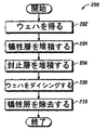
- ウェハ上に取り付けられた少なくとも1つのセンサエレメントを備えた該ウェハ上に第1の所定の厚さで、前記少なくとも1つのセンサエレメント上に少なくとも部分的に犠牲材料を堆積させるステップと、
前記ウェハ上で、前記堆積された犠牲材料の周りに前記第1の所定の厚さよりも薄い第2の所定の厚さで封止層を形成するステップと、
前記犠牲材料を除去するステップと
を有することを特徴とするセンサを製造する方法。 - 前記除去するステップの前に、
複数のチップを形成するために前記ウェハをダイシングするステップ
を更に有することを特徴とする請求項1に記載の方法。 - 前記堆積させるステップの後に、前記ウェハおよび前記堆積された犠牲材料を硬化させるステップを更に有することを特徴とする請求項1に記載の方法。
- 前記堆積させるステップが、揺変性の特性を備え、少なくとも約140℃の温度に耐える能力を備えた材料を堆積させることを更に含むことを特徴とする請求項1に記載の方法。
- 前記材料を堆積させるステップが、一時的に、水溶性熱可塑性接着材料を堆積させることを更に含むことを特徴とする請求項4に記載の方法。
- 前記堆積させるステップが、前記ウェハ上にニードルから前記犠牲材料を分配することを含むことを特徴とする請求項1に記載の方法。
- 前記堆積させるステップが、前記ウェハ上にマスクを配置することを含み、
前記マスクは、少なくとも1つの前記センサエレメントを露出させ、前記マスクの上から前記犠牲材料をシルクスクリーンさせることを特徴とする請求項1に記載の方法。 - 前記封止層を形成するステップが、前記封止層を形成するための液体モールディング技術を使用することを含むことを特徴とする請求項1に記載の方法。
- 前記除去するステップが、前記犠牲材料に溶液を適用することを含むことを特徴とする請求項1に記載の方法。
- 前記除去するステップが、前記犠牲材料の上に高圧脱イオン水をスプレーすることを含むことを特徴とする請求項9に記載の方法。
- 前記除去するステップが、前記犠牲材料にフォトレジストを適用することを含むことを特徴とする請求項9に記載の方法。
- 前記除去するステップが、前記犠牲材料にプラズマを適用することを含むことを特徴とする請求項9に記載の方法。
- 前記犠牲材料を除去するステップの後に、
前記ウェハを回路ボードに結合させるステップを更に有することを特徴とする請求項1に記載の方法。 - ウェハ上に取り付けられた少なくとも1つのセンサエレメントを備えた前記ウェハ上に第1の所定の厚さで犠牲材料を堆積させるステップと、を有し、
前記犠牲材料は、揺変性の特性を備え、少なくとも約140℃の温度に耐える能力を備え、少なくとも1つのセンサエレメント上の少なくとも一部に堆積され、
前記ウェハ上で、前記堆積された犠牲材料の周りに前記第1の所定の厚さよりも薄い代2の所定の厚さで封止層を形成するステップと、
前記犠牲材料を除去するステップと、
を有することを特徴とするセンサを製造する方法。 - 前記堆積させるステップが、前記ウェハ上にニードルから前記犠牲材料を分配させることを含むことを特徴とする請求項14に記載の方法。
- 前記堆積させるステップが、
前記ウェハ上にマスクを配置させることを有し、
前記マスクは少なくとも前記センサエレメントの1つを露出させ、前記マスクの上に前記犠牲材料をシルクスクリーンすることを特徴とする請求項14に記載の方法。 - 前記封止層を形成するステップが、前記封止層を形成するための液体モールディング技術を使用することを含むことを特徴とする請求項14に記載の方法。
- 前記除去するステップが、前記犠牲材料に対して溶液を適用することを含むことを特徴とする請求項14に記載の方法。
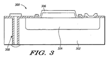
- 第1と第2の側を備えたウェハと、を有し、
前記第1の側の表面で露出された端を備えた相互接続が、第1の側と第2の側との間に延び、
前記ウェハの第2の側に結合したセンサエレメントと、
前記ウェハの第2の側に結合した封止層と、を有し
前記封止層が、貫通して延びる開口部を備え、前記センサエレメントを露出させるようにセンサの上に配置される、
ことを特徴とするセンサ。 - 前記封止層が、プラスチック、ポリイミド、または、絶縁体からなることを特徴とする請求項19に記載のセンサ。
Applications Claiming Priority (2)
| Application Number | Priority Date | Filing Date | Title |
|---|---|---|---|
| US11/039,688 US7109055B2 (en) | 2005-01-20 | 2005-01-20 | Methods and apparatus having wafer level chip scale package for sensing elements |
| PCT/US2005/045204 WO2006078374A1 (en) | 2005-01-20 | 2005-12-14 | Methods and apparatus having wafer level chip scale package for sensing elements |
Publications (2)
| Publication Number | Publication Date |
|---|---|
| JP2008529273A true JP2008529273A (ja) | 2008-07-31 |
| JP2008529273A5 JP2008529273A5 (ja) | 2009-02-12 |
Family
ID=36684436
Family Applications (1)
| Application Number | Title | Priority Date | Filing Date |
|---|---|---|---|
| JP2007552128A Pending JP2008529273A (ja) | 2005-01-20 | 2005-12-14 | 検知エレメントに関するウェハレベルチップスケールパッケージを備えた装置および方法 |
Country Status (7)
| Country | Link |
|---|---|
| US (1) | US7109055B2 (ja) |
| EP (1) | EP1842224A4 (ja) |
| JP (1) | JP2008529273A (ja) |
| KR (1) | KR101174937B1 (ja) |
| CN (1) | CN101065826A (ja) |
| TW (1) | TWI392032B (ja) |
| WO (1) | WO2006078374A1 (ja) |
Cited By (1)
| Publication number | Priority date | Publication date | Assignee | Title |
|---|---|---|---|---|
| JP2011220865A (ja) * | 2010-04-09 | 2011-11-04 | Alps Electric Co Ltd | フォースセンサパッケージ及びその製造方法 |
Families Citing this family (36)
| Publication number | Priority date | Publication date | Assignee | Title |
|---|---|---|---|---|
| TWI313501B (en) * | 2006-03-22 | 2009-08-11 | Ind Tech Res Inst | A process for manufacture plastic package of mems devices and the structure for the same |
| US7632698B2 (en) | 2006-05-16 | 2009-12-15 | Freescale Semiconductor, Inc. | Integrated circuit encapsulation and method therefor |
| WO2008005547A2 (en) * | 2006-07-05 | 2008-01-10 | Microstrain, Inc. | Rfid tag packaging system |
| US8153016B2 (en) | 2007-10-03 | 2012-04-10 | Apple Inc. | Shaping a cover glass |
| US8035216B2 (en) * | 2008-02-22 | 2011-10-11 | Intel Corporation | Integrated circuit package and method of manufacturing same |
| TWI398934B (zh) * | 2008-04-15 | 2013-06-11 | Analog Devices Inc | 晶圓級csp感測器 |
| US8037771B2 (en) * | 2009-05-13 | 2011-10-18 | Lsi Corporation | Electronic pressure-sensing device |
| US20110108999A1 (en) * | 2009-11-06 | 2011-05-12 | Nalla Ravi K | Microelectronic package and method of manufacturing same |
| US8742561B2 (en) | 2009-12-29 | 2014-06-03 | Intel Corporation | Recessed and embedded die coreless package |
| US8901724B2 (en) | 2009-12-29 | 2014-12-02 | Intel Corporation | Semiconductor package with embedded die and its methods of fabrication |
| US8535989B2 (en) | 2010-04-02 | 2013-09-17 | Intel Corporation | Embedded semiconductive chips in reconstituted wafers, and systems containing same |
| US8319318B2 (en) | 2010-04-06 | 2012-11-27 | Intel Corporation | Forming metal filled die back-side film for electromagnetic interference shielding with coreless packages |
| US8618652B2 (en) | 2010-04-16 | 2013-12-31 | Intel Corporation | Forming functionalized carrier structures with coreless packages |
| US8939347B2 (en) | 2010-04-28 | 2015-01-27 | Intel Corporation | Magnetic intermetallic compound interconnect |
| US9847308B2 (en) | 2010-04-28 | 2017-12-19 | Intel Corporation | Magnetic intermetallic compound interconnect |
| US8313958B2 (en) | 2010-05-12 | 2012-11-20 | Intel Corporation | Magnetic microelectronic device attachment |
| US8434668B2 (en) | 2010-05-12 | 2013-05-07 | Intel Corporation | Magnetic attachment structure |
| US8609532B2 (en) | 2010-05-26 | 2013-12-17 | Intel Corporation | Magnetically sintered conductive via |
| US20120001339A1 (en) | 2010-06-30 | 2012-01-05 | Pramod Malatkar | Bumpless build-up layer package design with an interposer |
| US8372666B2 (en) | 2010-07-06 | 2013-02-12 | Intel Corporation | Misalignment correction for embedded microelectronic die applications |
| US8754516B2 (en) | 2010-08-26 | 2014-06-17 | Intel Corporation | Bumpless build-up layer package with pre-stacked microelectronic devices |
| US8304913B2 (en) | 2010-09-24 | 2012-11-06 | Intel Corporation | Methods of forming fully embedded bumpless build-up layer packages and structures formed thereby |
| US8937382B2 (en) | 2011-06-27 | 2015-01-20 | Intel Corporation | Secondary device integration into coreless microelectronic device packages |
| US8848380B2 (en) | 2011-06-30 | 2014-09-30 | Intel Corporation | Bumpless build-up layer package warpage reduction |
| DE102011083719B4 (de) * | 2011-09-29 | 2022-12-08 | Robert Bosch Gmbh | Verfahren zur Herstellung einer Zweichipanordnung |
| WO2013106442A1 (en) | 2012-01-10 | 2013-07-18 | Hzo, Inc. | Masks for use in applying protective coatings to electronic assemblies, masked electronic assemblies and associated methods |
| JP5999302B2 (ja) | 2012-02-09 | 2016-09-28 | セイコーエプソン株式会社 | 電子デバイスおよびその製造方法、並びに電子機器 |
| JP5983912B2 (ja) * | 2012-02-09 | 2016-09-06 | セイコーエプソン株式会社 | 電子デバイスおよびその製造方法、並びに電子機器 |
| US9257368B2 (en) | 2012-05-14 | 2016-02-09 | Intel Corporation | Microelectric package utilizing multiple bumpless build-up structures and through-silicon vias |
| DE112012006469B4 (de) | 2012-06-08 | 2022-05-05 | Intel Corporation | Mikroelektronisches Gehäuse mit nicht komplanaren gekapselten mikroelektronischen Bauelementen und einer Aufbauschicht ohne Kontaktierhügel |
| US20130335898A1 (en) | 2012-06-18 | 2013-12-19 | Hzo, Inc. | Systems and methods for applying protective coatings to internal surfaces of fully assembled electronic devices |
| US9894776B2 (en) | 2013-01-08 | 2018-02-13 | Hzo, Inc. | System for refurbishing or remanufacturing an electronic device |
| US10449568B2 (en) | 2013-01-08 | 2019-10-22 | Hzo, Inc. | Masking substrates for application of protective coatings |
| JP6034884B2 (ja) | 2013-01-08 | 2016-11-30 | エイチズィーオー・インコーポレーテッド | 基板からの保護被覆選択部分の除去 |
| US9595485B2 (en) * | 2014-06-26 | 2017-03-14 | Nxp Usa, Inc. | Microelectronic packages having embedded sidewall substrates and methods for the producing thereof |
| EP3153851B1 (en) * | 2015-10-06 | 2024-05-01 | Carrier Corporation | Mems die with sensing structures |
Citations (3)
| Publication number | Priority date | Publication date | Assignee | Title |
|---|---|---|---|---|
| JPH10144707A (ja) * | 1996-11-05 | 1998-05-29 | Nippon Retsuku Kk | 電子部品の製造方法 |
| JP2003282791A (ja) * | 2002-03-20 | 2003-10-03 | Fujitsu Ltd | 接触型センサ内蔵半導体装置及びその製造方法 |
| US20040118214A1 (en) * | 2002-12-23 | 2004-06-24 | Motorola, Inc. | Method and structure for fabricating sensors with a sacrificial gel dome |
Family Cites Families (14)
| Publication number | Priority date | Publication date | Assignee | Title |
|---|---|---|---|---|
| US5445559A (en) * | 1993-06-24 | 1995-08-29 | Texas Instruments Incorporated | Wafer-like processing after sawing DMDs |
| US5511428A (en) * | 1994-06-10 | 1996-04-30 | Massachusetts Institute Of Technology | Backside contact of sensor microstructures |
| JP2001227902A (ja) * | 2000-02-16 | 2001-08-24 | Mitsubishi Electric Corp | 半導体装置 |
| US6335224B1 (en) * | 2000-05-16 | 2002-01-01 | Sandia Corporation | Protection of microelectronic devices during packaging |
| EP1211722B9 (en) * | 2000-11-30 | 2005-07-13 | STMicroelectronics S.r.l. | Manufacturing method of electronic device package |
| US6995034B2 (en) * | 2000-12-07 | 2006-02-07 | Reflectivity, Inc | Methods for depositing, releasing and packaging micro-electromechanical devices on wafer substrates |
| US6472243B2 (en) * | 2000-12-11 | 2002-10-29 | Motorola, Inc. | Method of forming an integrated CMOS capacitive pressure sensor |
| US6432737B1 (en) * | 2001-01-03 | 2002-08-13 | Amkor Technology, Inc. | Method for forming a flip chip pressure sensor die package |
| US6635509B1 (en) * | 2002-04-12 | 2003-10-21 | Dalsa Semiconductor Inc. | Wafer-level MEMS packaging |
| US7071032B2 (en) * | 2002-08-01 | 2006-07-04 | Taiwan Semiconductor Manufacturing Co., Ltd. | Material to improve image sensor yield during wafer sawing |
| DE10246283B3 (de) * | 2002-10-02 | 2004-03-25 | Infineon Technologies Ag | Verfahren zur Herstellung von Kanälen und Kavitäten in Halbleitergehäusen und elektronisches Bauteil mit derartigen Kanälen und Kavitäten |
| DE10316776B4 (de) * | 2003-04-11 | 2005-03-17 | Infineon Technologies Ag | Verfahren zum Erzeugen einer Schutzabdeckung für ein Bauelement |
| US6951769B2 (en) * | 2003-06-04 | 2005-10-04 | Texas Instruments Incorporated | Method for stripping sacrificial layer in MEMS assembly |
| US7091058B2 (en) * | 2003-12-11 | 2006-08-15 | Omnivision Technologies, Inc. | Sacrificial protective layer for image sensors and method of using |
-
2005
- 2005-01-20 US US11/039,688 patent/US7109055B2/en active Active
- 2005-12-14 CN CNA2005800400747A patent/CN101065826A/zh active Pending
- 2005-12-14 WO PCT/US2005/045204 patent/WO2006078374A1/en active Application Filing
- 2005-12-14 EP EP05854003A patent/EP1842224A4/en not_active Withdrawn
- 2005-12-14 KR KR1020077016574A patent/KR101174937B1/ko active IP Right Grant
- 2005-12-14 JP JP2007552128A patent/JP2008529273A/ja active Pending
- 2005-12-27 TW TW094146740A patent/TWI392032B/zh active
Patent Citations (3)
| Publication number | Priority date | Publication date | Assignee | Title |
|---|---|---|---|---|
| JPH10144707A (ja) * | 1996-11-05 | 1998-05-29 | Nippon Retsuku Kk | 電子部品の製造方法 |
| JP2003282791A (ja) * | 2002-03-20 | 2003-10-03 | Fujitsu Ltd | 接触型センサ内蔵半導体装置及びその製造方法 |
| US20040118214A1 (en) * | 2002-12-23 | 2004-06-24 | Motorola, Inc. | Method and structure for fabricating sensors with a sacrificial gel dome |
Cited By (1)
| Publication number | Priority date | Publication date | Assignee | Title |
|---|---|---|---|---|
| JP2011220865A (ja) * | 2010-04-09 | 2011-11-04 | Alps Electric Co Ltd | フォースセンサパッケージ及びその製造方法 |
Also Published As
| Publication number | Publication date |
|---|---|
| CN101065826A (zh) | 2007-10-31 |
| WO2006078374A1 (en) | 2006-07-27 |
| TWI392032B (zh) | 2013-04-01 |
| US7109055B2 (en) | 2006-09-19 |
| US20060160264A1 (en) | 2006-07-20 |
| TW200711007A (en) | 2007-03-16 |
| EP1842224A1 (en) | 2007-10-10 |
| KR101174937B1 (ko) | 2012-08-17 |
| KR20070095959A (ko) | 2007-10-01 |
| EP1842224A4 (en) | 2012-07-04 |
Similar Documents
| Publication | Publication Date | Title |
|---|---|---|
| JP2008529273A (ja) | 検知エレメントに関するウェハレベルチップスケールパッケージを備えた装置および方法 | |
| US9893213B2 (en) | Method of forming a wire bond sensor package | |
| CN109844938B (zh) | 具有增强性能的晶片级封装 | |
| US10157811B2 (en) | Chip package and method for forming the same | |
| TWI512930B (zh) | 晶片封裝體及其形成方法 | |
| CN103426838B (zh) | 晶片封装体及其形成方法 | |
| US20050205977A1 (en) | Methods and apparatus for packaging integrated circuit devices | |
| US8900924B2 (en) | Chip package and method for forming the same | |
| US9082681B2 (en) | Adhesive bonding technique for use with capacitive micro-sensors | |
| CN109801893A (zh) | 半导体装置 | |
| US9799588B2 (en) | Chip package and manufacturing method thereof | |
| KR101219619B1 (ko) | 웨이퍼 레벨에서의 반도체 패키징 방법 | |
| US9546089B1 (en) | Pressure sensor and packaging method thereof | |
| US20220221363A1 (en) | Pressure Sensor Device and Method for Forming a Pressure Sensor Device | |
| CN104701332A (zh) | 具有冷却特征的传感器封装和制造其的方法 | |
| US20040166662A1 (en) | MEMS wafer level chip scale package | |
| CN107369695B (zh) | 晶片封装体与其制造方法 | |
| US10118816B2 (en) | Method of forming a protective coating for a packaged semiconductor device | |
| TW201709447A (zh) | 感測模組及其製造方法 | |
| US7911043B2 (en) | Wafer level device package with sealing line having electroconductive pattern and method of packaging the same | |
| TWI588954B (zh) | 晶片封裝體及其製造方法 |
Legal Events
| Date | Code | Title | Description |
|---|---|---|---|
| A521 | Request for written amendment filed |
Free format text: JAPANESE INTERMEDIATE CODE: A523 Effective date: 20081215 |
|
| A621 | Written request for application examination |
Free format text: JAPANESE INTERMEDIATE CODE: A621 Effective date: 20081215 |
|
| A977 | Report on retrieval |
Free format text: JAPANESE INTERMEDIATE CODE: A971007 Effective date: 20110511 |
|
| A131 | Notification of reasons for refusal |
Free format text: JAPANESE INTERMEDIATE CODE: A131 Effective date: 20110519 |
|
| A521 | Request for written amendment filed |
Free format text: JAPANESE INTERMEDIATE CODE: A523 Effective date: 20110819 |
|
| RD04 | Notification of resignation of power of attorney |
Free format text: JAPANESE INTERMEDIATE CODE: A7424 Effective date: 20110915 |
|
| A02 | Decision of refusal |
Free format text: JAPANESE INTERMEDIATE CODE: A02 Effective date: 20120130 |