JP2008529273A - Apparatus and method with wafer level chip scale package for sensing element - Google Patents
Apparatus and method with wafer level chip scale package for sensing element Download PDFInfo
- Publication number
- JP2008529273A JP2008529273A JP2007552128A JP2007552128A JP2008529273A JP 2008529273 A JP2008529273 A JP 2008529273A JP 2007552128 A JP2007552128 A JP 2007552128A JP 2007552128 A JP2007552128 A JP 2007552128A JP 2008529273 A JP2008529273 A JP 2008529273A
- Authority
- JP
- Japan
- Prior art keywords
- wafer
- sacrificial material
- sensor
- depositing
- sealing layer
- Prior art date
- Legal status (The legal status is an assumption and is not a legal conclusion. Google has not performed a legal analysis and makes no representation as to the accuracy of the status listed.)
- Pending
Links
Images


Classifications
-
- H—ELECTRICITY
- H01—ELECTRIC ELEMENTS
- H01L—SEMICONDUCTOR DEVICES NOT COVERED BY CLASS H10
- H01L21/00—Processes or apparatus adapted for the manufacture or treatment of semiconductor or solid state devices or of parts thereof
-
- B—PERFORMING OPERATIONS; TRANSPORTING
- B81—MICROSTRUCTURAL TECHNOLOGY
- B81C—PROCESSES OR APPARATUS SPECIALLY ADAPTED FOR THE MANUFACTURE OR TREATMENT OF MICROSTRUCTURAL DEVICES OR SYSTEMS
- B81C1/00—Manufacture or treatment of devices or systems in or on a substrate
- B81C1/00015—Manufacture or treatment of devices or systems in or on a substrate for manufacturing microsystems
- B81C1/00261—Processes for packaging MEMS devices
- B81C1/00309—Processes for packaging MEMS devices suitable for fluid transfer from the MEMS out of the package or vice versa, e.g. transfer of liquid, gas, sound
-
- B—PERFORMING OPERATIONS; TRANSPORTING
- B81—MICROSTRUCTURAL TECHNOLOGY
- B81C—PROCESSES OR APPARATUS SPECIALLY ADAPTED FOR THE MANUFACTURE OR TREATMENT OF MICROSTRUCTURAL DEVICES OR SYSTEMS
- B81C2201/00—Manufacture or treatment of microstructural devices or systems
- B81C2201/05—Temporary protection of devices or parts of the devices during manufacturing
- B81C2201/053—Depositing a protective layers
Landscapes
- Engineering & Computer Science (AREA)
- Microelectronics & Electronic Packaging (AREA)
- Manufacturing & Machinery (AREA)
- Physics & Mathematics (AREA)
- Condensed Matter Physics & Semiconductors (AREA)
- General Physics & Mathematics (AREA)
- Computer Hardware Design (AREA)
- Power Engineering (AREA)
- Pressure Sensors (AREA)
- Measuring Fluid Pressure (AREA)
- Encapsulation Of And Coatings For Semiconductor Or Solid State Devices (AREA)
Abstract
センサ(100)を製造するための方法を提供する。該方法は、ウェハ上に取り付けられた少なくとも1つのセンサエレメントを備えた該ウェハ上に第1の所定の厚さで犠牲材料(330)を堆積させ、該犠牲材料は少なくとも1つのセンサエレメント上の少なくとも一部に堆積され、前記ウェハ上で、堆積された犠牲材料の周りに第1の所定の厚さよりも薄い第2の所定の厚さで封止層(332)を形成し、犠牲材料を除去することを有する。上述の方法により製造されたセンサのための装置も提供される。 A method for manufacturing a sensor (100) is provided. The method deposits a sacrificial material (330) at a first predetermined thickness on the wafer with at least one sensor element mounted on the wafer, the sacrificial material on the at least one sensor element. Forming a sealing layer (332) on the wafer at a second predetermined thickness less than the first predetermined thickness on the wafer and deposited around the deposited sacrificial material; Have to remove. An apparatus for a sensor manufactured by the method described above is also provided.
Description
本発明は一般的にはチップパッケージングに関し、特にウェハレベルチップスケールパッケージに関する。 The present invention relates generally to chip packaging, and more particularly to wafer level chip scale packages.
センサは、無数の用途に使用され、多数のタイプのデータを収集するのに使用されうる。あるセンサは、例えば参照圧力と測定された圧力との間、または、2つの測定された圧力の間の圧力差を判断するのに用いられる。典型的には、これらの圧力センサは、そこに印刷された回路、および/または、そこに取り付けられた他のコンポーネントを備えた集積されたチップを含む。あるセンサ構成では、チップは、センサコンポーネントを保護し、チップ作動中の回路によって生成される熱を放散させるように構成されたハードケース内に配置される。他のセンサ構成では、チップはまた、ダイを回路ボードに取り付けるために使用される複数のボンドワイヤを含む。ボンドワイヤは典型的には、チップからケースの外に延びる。 Sensors are used in myriad applications and can be used to collect multiple types of data. Some sensors are used, for example, to determine a pressure difference between a reference pressure and a measured pressure, or between two measured pressures. These pressure sensors typically include an integrated chip with circuitry printed thereon and / or other components attached thereto. In some sensor configurations, the chip is placed in a hard case that is configured to protect the sensor components and dissipate the heat generated by the circuit during chip operation. In other sensor configurations, the chip also includes a plurality of bond wires that are used to attach the die to the circuit board. The bond wire typically extends out of the case from the chip.
上述のセンサ構成は一般的には殆どの用途で良好に作動するけれども、他の用途では所定の欠点から不利益を被る。例えば、医療用デバイス関連では、移植可能異物の医療用デバイスに使用されるコンポーネントは、インプラント患者によって経験されうる不快を低減させるために可能な限り極めて小さい。しかしながら、上述したこれらのようなケースを備えた在来のセンサは、比較的高い高さ、および/または、大きなフットプリントを有しており、そのため、インプラント可能な医療用デバイスから除かれうるスペースを不必要に占める。他の例では、上述のチップは、製造するのに比較的高価である。その結果、比較的安価なコンポーネントは、センサチップ技術に組み入れられず、また、別の実施形態では、該チップが組み入れられるならば、コンポーネントの費用は増大する。 While the sensor arrangements described above generally work well for most applications, other applications suffer from certain drawbacks. For example, in the context of medical devices, the components used in implantable foreign medical devices are as small as possible to reduce discomfort that can be experienced by an implant patient. However, conventional sensors with cases like those described above have a relatively high height and / or a large footprint, so that space that can be removed from an implantable medical device. Occupy unnecessarily. In other examples, the above-described chip is relatively expensive to manufacture. As a result, relatively inexpensive components are not incorporated into sensor chip technology, and in other embodiments, the cost of the component increases if the chip is incorporated.
従って、在来の集積チップパッケージと比較して相対的に小さい集積チップパッケージを有することが望まれる。さらに、製造するのに相対的にシンプルで高価でない集積コンポーネントを作るための方法が望まれる。さらに、本発明の他の望ましい特徴および特性は、この発明の背景と添付の図面を参照して、発明の詳細な説明および特許請求の範囲から明らかになるであろう。 It is therefore desirable to have an integrated chip package that is relatively small compared to conventional integrated chip packages. Furthermore, a method is desired for making integrated components that are relatively simple and inexpensive to manufacture. Furthermore, other desirable features and characteristics of the present invention will become apparent from the detailed description of the invention and the claims, taken in conjunction with the background of the invention and the accompanying drawings.
かくして、在来の集積チップパッケージと比較して相対的に小さい集積チップスケールパッケージを提供する。更に、相対的に安価でシンプルであるチップスケールパッケージングを処理するための方法が提供される。 Thus, an integrated chip scale package that is relatively small compared to conventional integrated chip packages is provided. Furthermore, a method is provided for processing chip scale packaging that is relatively inexpensive and simple.
以下の本発明の詳細な説明は、単に例示的なものであり、本発明の使用及び用途を限定するものではない。更に、上記背景技術に示したいかなる理論によっても本発明は制限されない。 The following detailed description of the invention is merely exemplary and is not intended to limit the use and application of the invention. Furthermore, the present invention is not limited by any theory presented in the background art.
図1を参照すると、典型的な集積コンポーネントまたはセンサ100の断面図が示されている。センサ100は、基板層102、回路104、センサエレメント106、相互接続108、および、封止層110を含む。基板層102は、センサコンポーネントが結合されるベースを提供する。伝統的に使用される基板は、例えば、シリコン、シリコンゲルマニウム、ガリウム砒素、シリコン−オン−絶縁体、絶縁ガラス、サファイア、または他の如何なる適切な材料を含み、基板層はそれらの種々のタイプの材料からなることを認識すべきであろう。回路104は、基板層102の少なくとも一部に配置され、例えば、通信、輸送、一般的な計算のような種々の集積回路の用途のために構成され得る。例えば、ある実施形態では、回路104は、圧力データと通信するように構成される。回路104は、例えば、スクリーン印刷、および、フォトリソグラフィーのような種々の在来の手段のいずれかで基板層102上に形成されうる。
Referring to FIG. 1, a cross-sectional view of a typical integrated component or
センサエレメント106は、センサ100の周りの環境特性を検知するように構成される。センサエレメント106は、環境の特定の特性を検知するように用いられ得る種々のタイプのデバイスの1つである。例えば、図1に例示した実施形態では、センサエレメント106は、キャビティ112を画定する薄いドーム形状のダイヤフラムであり、その下に、キャビティ112内の圧力と環境圧力との間の圧力差に応答するように延び、または、接触する。
検知された特性を処理するために、センサエレメント106は、回路104に接続される。センサエレメント106は、種々の在来の仕方の1つで回路104に直接または間接的に結合されうる。センサエレメント106はまた、参照データを提供するリファレンスエレメント107に結合されうる。リファレンスエレメント107は、参照データを提供するために適当な種々のデバイスの1つであって良い。図1に例示された実施形態では、リファレンスエレメント107は、参照圧力を提供するように構成されたドーム形状のダイヤフラムである。更に、リファレンスエレメント107は、センサエレメント106の隣に配置するように示されるが、リファレンスエレメント107がセンサ100の他の部分に結合されうることも明らかであろう。図1の実施形態では、回路104は、参照圧力と検知された環境圧力との間の差を計算するように構成される。
The
相互接続108により、回路104は、センサエレメント106によって検知されたデータ、および/または、センサエレメント106とリファレンスエレメント107との間の計算された差を、他の図示されていない外部コンポーネントと通信させることができる。これに関して、相互接続108は、データを送信および受信するために、例えば、金属またはポリシリコンのような適当な種々の材料のうちの1つから構成される。相互接続108は、基板層102を貫通して形成された通路120内の少なくとも一部に配置される。しかしながら、相互接続108は、センサ100のいかなる部分にも位置決めされない。単一の相互接続108と通路120を図示したけれども、それぞれ1つ以上のものがセンサ100に組み入れられても良いことは明らかである。
Interconnect 108 allows
相互接続108は、第1の端114と第2の端116とを有する。第1の端114は、回路104に接続され、相互接続108の一方の端に形成されてもよく、若しくは、図1に図示したように、相互接続108に続いて結合される別に形成された部分であっても良い。別のケースでは、第1の端114は、電気通信をすることが出来る伝導材料から構成される。第2の端116は、センサ100まで外部に延び、センサ100と、例えば回路ボード、モジュールハウジング、または、基板のようなものと結合されうるセンサ100に対する外部コンポーネントとの間のインターフェースを提供する。第1の端114と同様に、第2の端116は、相互接続108の一部として形成されても良く、または、別の実施形態として、図1に示したように、別に形成された部分であってもよい。図1に例示したように、第2の端116は、相互接続108に接続された平らな部分122と、平らな部分122に接続された伝導部分124とを備えた伝導材料の一部である。伝導部分124は、センサ100から外側に向けてさら形である。相互接続108と回路104との間に生じる可能性がある電気的接続の交差を防ぐために、パッシベーション層126が、基板層102と通路120との上に横たわる。パッシベーション層126は、例えば、パリレン、二酸化シリコン、窒化シリコンなどのような多数の絶縁材料のうちの1つから構成されうる。
The
封止層110は、化学的、物理的、熱的、および/または、他のいかなるタイプのダメージから回路104を保護するのに採用される。これに関して、封止層110は、センサ100が配置されるいかなる化学的、物理的、または、熱的環境に耐えることができる種々の封止材料から構成される。適当な材料は、プラスチック、硬質ポリマー、ポリイミドなどのようなものを含むが、それらに限定されない。センサエレメント106を環境に接触させることが出来るように、開口部128がそこに設けられる。開口部128は、センサエレメント106が実質的に露出されているセンサエレメント106の上に位置決めされる。別の実施形態では、センサエレメント106は、図1に示したように開口部128内に配置される。更に、開口部128は、リファレンスエレメント107の上に配置され、または、リファレンスエレメント107は、開口部128内に位置決めされうる。ある実施形態では、開口部128は、封止層110がセンサエレメント106と接触しないように寸法決めされる。
The sealing
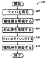
図2乃至6を参照すると、集積されたコンポーネント100が製造される例示の方法が開示されている。全体のプロセス200がまず全体的に記載される。以下の記述において挿入されるリファレンスは、図2に示されたフローチャートブロックに関連する参照番号に対応することを理解すべきである。まず、基板層302、回路304、少なくとも1つのセンサエレメント306、および、少なくとも1つの相互接続308を備えたウェハ300を用意する(202)。次いで、犠牲層330が各センサエレメント306の上に配置される(204)。次いで、封止層332がウェハ300に適用される(206)。ウェハ300は次いで、ダイシングされる(208)。最後に、犠牲層330が除去される(210)。これらのステップを以下に更に詳細に記載する。
With reference to FIGS. 2-6, an exemplary method by which an integrated
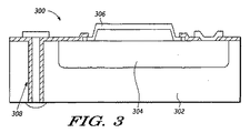
図3を参照すると、用意することができ得る(202)典型的なウェハ300の一部が図示されている。ウェハ部分300は、基板層302、その上に印刷またはスクリーン(シルクスクリーン印刷)された回路304、回路に結合された少なくとも1つのセンサエレメント306、ウェハ部分300を通って延びる相互接続308を含む。ウェハ部分300は、1つ以上のウェハ部分300を含むウェハの一部である。ウェハは、例えば、フォトリソグラフィー、化学気相蒸着(CVD)、物理的CVD、化学機械的平坦化、および/または、化学的エッチングを含むが、それらに限定されない表面製造技術と、バックエンド製造技術を使用してウェハを製造する種々の在来の方法でプロセス200の一部として製造される。別の実施形態では、ウェハ300は、プロセス200の前に用意されうる。
Referring to FIG. 3, a portion of a
簡単に上述したように、次いで、図4に示したように犠牲層330が各センサエレメント306の上に配置される(204)。堆積は、種々の仕方で実行されうる。例えばある実施形態では、犠牲層材料は、適当に形成されたニードルを使用して各センサエレメント306の上に配置される。別の実施形態では、適当に構成されたマスクが、ウェハ300の上に配置され、犠牲層材料は、マスクおよびウェハ300の上にスクリーンされる。更に別の実施形態では、犠牲層材料は、シャドウマスクおよびスプレー、または、アプリケーションのスピンを使用して配置されうる。犠牲層330は、少なくともセンサエレメント106が完全に被覆されるように配置されるのが好ましい。ある実施形態では、犠牲層330は、約0.020と2mmとの間の厚さで配置される。別の実施形態では、犠牲層330は、結果としてのセンサ100の厚さの約10%の厚さであって良い。しかしながら、他の適合な厚さも同様に採用することができ得る。
As briefly described above, a
犠牲層材料は、ダメージ無くセンサエレメント306に対して一時的に接着するのに適当な種々の材料であってよい。材料は、揺変性で、少なくとも140℃、または、プロセス200で採用されうる他のいかなる温度でも硬化することなく、分解することなく次のダイシングステップ(208)を耐えることができるものが好ましい。更に、材料は、除去溶液または除去プロセスの適用の際に容易に除去可能なものであるのが好ましい。ある実施形態では、犠牲材料は、水溶性で、脱イオン水の適用で除去可能である。別の実施形態では、材料は、フォトレジストストリッパ、または、他の化学的若しくはプラズマ材料を使用することにより除去される。適当な犠牲層材料は、米国カリフォルニア州PlacentiaのAquabond, LLCによって提供されるAquabond S65、または、コネチカットのDymaxコーポレーションによって提供されるDymax 9−20553を含むが、それらの接着剤に限定されるわけではない。いつかの材料では、センサエレメント306の上に犠牲層330を十分にセットするために、硬化を生じさせる必要があり得る。犠牲層330が、センサエレメント306の上に堆積されるようにここでは記載されるけれども、堆積は、保護される必要のない他のウェハ取り付けコンポーネント上でも生じうることは明らかであろう。
The sacrificial layer material can be a variety of materials suitable for temporary adhesion to the
犠牲層材料が堆積された後、封止層332がウェハ300の上に形成される(206)。図5に図示したように、封止層332は、液体モールディング技術を含むが、それには限定されない、ウェハを封止する種々の在来の仕方を使用して形成されうる。例えば、ウェハレベルモールディング技術が用いられてもよい。ある実施形態では、封止層材料からなるペレットが、ウェハ上に配置され、ウェハ300は2つのホットプラテンの間に取り付けられる。ホットプラテンが互いに近づいてきて、プラテンからの熱によって、封止層材料がウェハ300の上で流れることが出来るようにペレットを溶かす。材料が犠牲層330の間のスペースに流れるように封止層材料の量が使用されるが、犠牲層330を包まないのが好ましい。封止層332を作るのに使用される材料は、回路の上を保護するように被覆する際に典型的に使用される種々の材料であって良い。例えば、封止層332は、プラスチック、エポキシ、ポリイミド、または、他のいかなる適当な絶縁材料のタイプからなっても良い。
After the sacrificial layer material is deposited, a
封止層332がウェハ300の上に適当に形成されたのち、ウェハ300はダイシングされる(208)。ダイシングステップ(208)中、ウェハ300は、図6に図示したように複数のダイまたはチップ300a,300b,300cに切断される。ダイシングは、ソー技術を採用するように、ダイシングの従来の方法を使用して実行されうる。封止ステップ(206)の後に行われる、ダイシングステップ(208)をここで記載したけれども、ダイシングは、例えばプロセス(200)の終わりのプロセス中に他の適当な接合で生じうることも明らかであろう。
After the
次いで、犠牲層330は、チップ300aから離される(210)。犠牲層330は、採用される犠牲層材料によって、脱イオン水、プラズマ、または、他のケミカルのような適当な除去溶液を使用して除去されうる。ある実施形態では、除去溶液は、高圧下に配置され、続いて、犠牲層330にスプレーされる。犠牲層300材料が除去されるとき、開口部338が形成されセンサエレメント308を露出し、その結果、図1に示したようなセンサ100が生じる。チップ300aは次いで、回路ボードまたは他の外部デバイスに取り付けられ得る。
The
かくして、在来の集積チップパッケージと比較して相対的に小さい集積チップスケールパッケージを提供する。更に、相対的に安価でシンプルであるチップスケールパッケージングを処理するための方法が提供される。 Thus, an integrated chip scale package that is relatively small compared to conventional integrated chip packages is provided. Furthermore, a method is provided for processing chip scale packaging that is relatively inexpensive and simple.
少なくとも1つの例示的な実施形態を詳細な説明で記載してきたが、莫大な数のバリエーションが存在することを理解すべきである。また実施形態は、単に例示なだけであり、いかなる場合においても本発明の範囲、適用、または構成を制限するものではない。むしろ、本発明の例示的な実施形態を実装するための便利なロードマップとして当業者は理解するものであり、本発明の範囲および均等の範囲は、添付の特許請求の範囲から判断されるべきであり、かかる範囲を逸脱することなく本発明の種々の変更をすることが出来ることを理解すべきである。 Although at least one exemplary embodiment has been described in the detailed description, it should be understood that a vast number of variations exist. Also, the embodiments are merely illustrative and do not limit the scope, application, or configuration of the invention in any way. Rather, those skilled in the art will appreciate that this is a convenient roadmap for implementing the exemplary embodiments of the present invention, and the scope and equivalent scope of the present invention should be determined from the appended claims. It should be understood that various modifications of the present invention can be made without departing from this scope.
Claims (20)
前記ウェハ上で、前記堆積された犠牲材料の周りに前記第1の所定の厚さよりも薄い第2の所定の厚さで封止層を形成するステップと、
前記犠牲材料を除去するステップと
を有することを特徴とするセンサを製造する方法。 Depositing at least partially a sacrificial material on the at least one sensor element at a first predetermined thickness on the wafer comprising at least one sensor element mounted on the wafer;
Forming a sealing layer on the wafer with a second predetermined thickness less than the first predetermined thickness around the deposited sacrificial material;
Removing the sacrificial material. A method of manufacturing a sensor.
複数のチップを形成するために前記ウェハをダイシングするステップ
を更に有することを特徴とする請求項1に記載の方法。 Before the removing step,
The method of claim 1, further comprising dicing the wafer to form a plurality of chips.
前記マスクは、少なくとも1つの前記センサエレメントを露出させ、前記マスクの上から前記犠牲材料をシルクスクリーンさせることを特徴とする請求項1に記載の方法。 The step of depositing comprises disposing a mask on the wafer;
The method of claim 1, wherein the mask exposes at least one of the sensor elements and silkscreens the sacrificial material over the mask.
前記ウェハを回路ボードに結合させるステップを更に有することを特徴とする請求項1に記載の方法。 After the step of removing the sacrificial material,
The method of claim 1, further comprising the step of bonding the wafer to a circuit board.
前記犠牲材料は、揺変性の特性を備え、少なくとも約140℃の温度に耐える能力を備え、少なくとも1つのセンサエレメント上の少なくとも一部に堆積され、
前記ウェハ上で、前記堆積された犠牲材料の周りに前記第1の所定の厚さよりも薄い代2の所定の厚さで封止層を形成するステップと、
前記犠牲材料を除去するステップと、
を有することを特徴とするセンサを製造する方法。 Depositing a sacrificial material at a first predetermined thickness on the wafer comprising at least one sensor element mounted on the wafer;
The sacrificial material has thixotropic properties, has the ability to withstand a temperature of at least about 140 ° C., and is deposited on at least a portion of at least one sensor element;
Forming a sealing layer on the wafer around the deposited sacrificial material at a predetermined thickness of thickness 2 that is less than the first predetermined thickness;
Removing the sacrificial material;
A method of manufacturing a sensor comprising:
前記ウェハ上にマスクを配置させることを有し、
前記マスクは少なくとも前記センサエレメントの1つを露出させ、前記マスクの上に前記犠牲材料をシルクスクリーンすることを特徴とする請求項14に記載の方法。 The depositing step comprises:
Having a mask disposed on the wafer;
15. The method of claim 14, wherein the mask exposes at least one of the sensor elements and silkscreens the sacrificial material over the mask.
前記第1の側の表面で露出された端を備えた相互接続が、第1の側と第2の側との間に延び、
前記ウェハの第2の側に結合したセンサエレメントと、
前記ウェハの第2の側に結合した封止層と、を有し
前記封止層が、貫通して延びる開口部を備え、前記センサエレメントを露出させるようにセンサの上に配置される、
ことを特徴とするセンサ。 A wafer having first and second sides;
An interconnect with an end exposed at the surface of the first side extending between the first side and the second side;
A sensor element coupled to a second side of the wafer;
A sealing layer coupled to a second side of the wafer, the sealing layer comprising an opening extending therethrough and disposed on the sensor to expose the sensor element;
A sensor characterized by that.
Applications Claiming Priority (2)
| Application Number | Priority Date | Filing Date | Title |
|---|---|---|---|
| US11/039,688 US7109055B2 (en) | 2005-01-20 | 2005-01-20 | Methods and apparatus having wafer level chip scale package for sensing elements |
| PCT/US2005/045204 WO2006078374A1 (en) | 2005-01-20 | 2005-12-14 | Methods and apparatus having wafer level chip scale package for sensing elements |
Publications (2)
| Publication Number | Publication Date |
|---|---|
| JP2008529273A true JP2008529273A (en) | 2008-07-31 |
| JP2008529273A5 JP2008529273A5 (en) | 2009-02-12 |
Family
ID=36684436
Family Applications (1)
| Application Number | Title | Priority Date | Filing Date |
|---|---|---|---|
| JP2007552128A Pending JP2008529273A (en) | 2005-01-20 | 2005-12-14 | Apparatus and method with wafer level chip scale package for sensing element |
Country Status (7)
| Country | Link |
|---|---|
| US (1) | US7109055B2 (en) |
| EP (1) | EP1842224A4 (en) |
| JP (1) | JP2008529273A (en) |
| KR (1) | KR101174937B1 (en) |
| CN (1) | CN101065826A (en) |
| TW (1) | TWI392032B (en) |
| WO (1) | WO2006078374A1 (en) |
Cited By (1)
| Publication number | Priority date | Publication date | Assignee | Title |
|---|---|---|---|---|
| JP2011220865A (en) * | 2010-04-09 | 2011-11-04 | Alps Electric Co Ltd | Force sensor package and manufacturing method of the same |
Families Citing this family (36)
| Publication number | Priority date | Publication date | Assignee | Title |
|---|---|---|---|---|
| TWI313501B (en) * | 2006-03-22 | 2009-08-11 | Ind Tech Res Inst | A process for manufacture plastic package of mems devices and the structure for the same |
| US7632698B2 (en) * | 2006-05-16 | 2009-12-15 | Freescale Semiconductor, Inc. | Integrated circuit encapsulation and method therefor |
| WO2008005547A2 (en) * | 2006-07-05 | 2008-01-10 | Microstrain, Inc. | Rfid tag packaging system |
| US8153016B2 (en) | 2007-10-03 | 2012-04-10 | Apple Inc. | Shaping a cover glass |
| US8035216B2 (en) * | 2008-02-22 | 2011-10-11 | Intel Corporation | Integrated circuit package and method of manufacturing same |
| WO2009129198A1 (en) * | 2008-04-15 | 2009-10-22 | Analog Devices, Inc. | Wafer level csp sensor |
| US8037771B2 (en) * | 2009-05-13 | 2011-10-18 | Lsi Corporation | Electronic pressure-sensing device |
| US20110108999A1 (en) * | 2009-11-06 | 2011-05-12 | Nalla Ravi K | Microelectronic package and method of manufacturing same |
| US8901724B2 (en) | 2009-12-29 | 2014-12-02 | Intel Corporation | Semiconductor package with embedded die and its methods of fabrication |
| US8742561B2 (en) | 2009-12-29 | 2014-06-03 | Intel Corporation | Recessed and embedded die coreless package |
| US8535989B2 (en) | 2010-04-02 | 2013-09-17 | Intel Corporation | Embedded semiconductive chips in reconstituted wafers, and systems containing same |
| US8319318B2 (en) | 2010-04-06 | 2012-11-27 | Intel Corporation | Forming metal filled die back-side film for electromagnetic interference shielding with coreless packages |
| US8618652B2 (en) | 2010-04-16 | 2013-12-31 | Intel Corporation | Forming functionalized carrier structures with coreless packages |
| US9847308B2 (en) | 2010-04-28 | 2017-12-19 | Intel Corporation | Magnetic intermetallic compound interconnect |
| US8939347B2 (en) | 2010-04-28 | 2015-01-27 | Intel Corporation | Magnetic intermetallic compound interconnect |
| US8313958B2 (en) | 2010-05-12 | 2012-11-20 | Intel Corporation | Magnetic microelectronic device attachment |
| US8434668B2 (en) | 2010-05-12 | 2013-05-07 | Intel Corporation | Magnetic attachment structure |
| US8609532B2 (en) | 2010-05-26 | 2013-12-17 | Intel Corporation | Magnetically sintered conductive via |
| US20120001339A1 (en) | 2010-06-30 | 2012-01-05 | Pramod Malatkar | Bumpless build-up layer package design with an interposer |
| US8372666B2 (en) | 2010-07-06 | 2013-02-12 | Intel Corporation | Misalignment correction for embedded microelectronic die applications |
| US8754516B2 (en) | 2010-08-26 | 2014-06-17 | Intel Corporation | Bumpless build-up layer package with pre-stacked microelectronic devices |
| US8304913B2 (en) | 2010-09-24 | 2012-11-06 | Intel Corporation | Methods of forming fully embedded bumpless build-up layer packages and structures formed thereby |
| US8937382B2 (en) | 2011-06-27 | 2015-01-20 | Intel Corporation | Secondary device integration into coreless microelectronic device packages |
| US8848380B2 (en) | 2011-06-30 | 2014-09-30 | Intel Corporation | Bumpless build-up layer package warpage reduction |
| DE102011083719B4 (en) * | 2011-09-29 | 2022-12-08 | Robert Bosch Gmbh | Method of manufacturing a two-chip device |
| US20130176691A1 (en) * | 2012-01-10 | 2013-07-11 | Hzo, Inc. | Masks for use in applying protective coatings to electronic assemblies, masked electronic assemblies and associated methods |
| JP5999302B2 (en) | 2012-02-09 | 2016-09-28 | セイコーエプソン株式会社 | Electronic device, manufacturing method thereof, and electronic apparatus |
| JP5983912B2 (en) * | 2012-02-09 | 2016-09-06 | セイコーエプソン株式会社 | Electronic device, manufacturing method thereof, and electronic apparatus |
| WO2013172814A1 (en) | 2012-05-14 | 2013-11-21 | Intel Corporation | Microelectronic package utilizing multiple bumpless build-up structures and through-silicon vias |
| CN104321864B (en) | 2012-06-08 | 2017-06-20 | 英特尔公司 | Microelectronics Packaging with the non-coplanar, microelectronic component of encapsulating and solderless buildup layer |
| KR20150020574A (en) | 2012-06-18 | 2015-02-26 | 에이치제트오 인코포레이티드 | Systems and methods for applying protective coatings to internal surfaces of fully assembled electronic devices |
| US10449568B2 (en) | 2013-01-08 | 2019-10-22 | Hzo, Inc. | Masking substrates for application of protective coatings |
| JP6034884B2 (en) | 2013-01-08 | 2016-11-30 | エイチズィーオー・インコーポレーテッド | Removal of selected protective coating from substrate |
| US9894776B2 (en) | 2013-01-08 | 2018-02-13 | Hzo, Inc. | System for refurbishing or remanufacturing an electronic device |
| US9595485B2 (en) * | 2014-06-26 | 2017-03-14 | Nxp Usa, Inc. | Microelectronic packages having embedded sidewall substrates and methods for the producing thereof |
| EP3153851B1 (en) * | 2015-10-06 | 2024-05-01 | Carrier Corporation | Mems die with sensing structures |
Citations (3)
| Publication number | Priority date | Publication date | Assignee | Title |
|---|---|---|---|---|
| JPH10144707A (en) * | 1996-11-05 | 1998-05-29 | Nippon Retsuku Kk | Manufacture of electronic component |
| JP2003282791A (en) * | 2002-03-20 | 2003-10-03 | Fujitsu Ltd | Semiconductor device with built-in contact-type sensor and manufacturing method thereof |
| US20040118214A1 (en) * | 2002-12-23 | 2004-06-24 | Motorola, Inc. | Method and structure for fabricating sensors with a sacrificial gel dome |
Family Cites Families (14)
| Publication number | Priority date | Publication date | Assignee | Title |
|---|---|---|---|---|
| US5445559A (en) * | 1993-06-24 | 1995-08-29 | Texas Instruments Incorporated | Wafer-like processing after sawing DMDs |
| US5511428A (en) * | 1994-06-10 | 1996-04-30 | Massachusetts Institute Of Technology | Backside contact of sensor microstructures |
| JP2001227902A (en) * | 2000-02-16 | 2001-08-24 | Mitsubishi Electric Corp | Semiconductor device |
| US6335224B1 (en) * | 2000-05-16 | 2002-01-01 | Sandia Corporation | Protection of microelectronic devices during packaging |
| EP1211722B9 (en) * | 2000-11-30 | 2005-07-13 | STMicroelectronics S.r.l. | Manufacturing method of electronic device package |
| US6995034B2 (en) * | 2000-12-07 | 2006-02-07 | Reflectivity, Inc | Methods for depositing, releasing and packaging micro-electromechanical devices on wafer substrates |
| US6472243B2 (en) * | 2000-12-11 | 2002-10-29 | Motorola, Inc. | Method of forming an integrated CMOS capacitive pressure sensor |
| US6432737B1 (en) * | 2001-01-03 | 2002-08-13 | Amkor Technology, Inc. | Method for forming a flip chip pressure sensor die package |
| US6635509B1 (en) * | 2002-04-12 | 2003-10-21 | Dalsa Semiconductor Inc. | Wafer-level MEMS packaging |
| US7071032B2 (en) * | 2002-08-01 | 2006-07-04 | Taiwan Semiconductor Manufacturing Co., Ltd. | Material to improve image sensor yield during wafer sawing |
| DE10246283B3 (en) * | 2002-10-02 | 2004-03-25 | Infineon Technologies Ag | Production of an electronic component used in semiconductor sensors comprises preparing a semiconductor chip on a switching substrate, applying a sacrificial part on the sensor region of the chip and further processing |
| DE10316776B4 (en) * | 2003-04-11 | 2005-03-17 | Infineon Technologies Ag | Method for producing a protective cover for a component |
| US6951769B2 (en) * | 2003-06-04 | 2005-10-04 | Texas Instruments Incorporated | Method for stripping sacrificial layer in MEMS assembly |
| US7091058B2 (en) * | 2003-12-11 | 2006-08-15 | Omnivision Technologies, Inc. | Sacrificial protective layer for image sensors and method of using |
-
2005
- 2005-01-20 US US11/039,688 patent/US7109055B2/en active Active
- 2005-12-14 CN CNA2005800400747A patent/CN101065826A/en active Pending
- 2005-12-14 KR KR1020077016574A patent/KR101174937B1/en active IP Right Grant
- 2005-12-14 WO PCT/US2005/045204 patent/WO2006078374A1/en active Application Filing
- 2005-12-14 EP EP05854003A patent/EP1842224A4/en not_active Withdrawn
- 2005-12-14 JP JP2007552128A patent/JP2008529273A/en active Pending
- 2005-12-27 TW TW094146740A patent/TWI392032B/en active
Patent Citations (3)
| Publication number | Priority date | Publication date | Assignee | Title |
|---|---|---|---|---|
| JPH10144707A (en) * | 1996-11-05 | 1998-05-29 | Nippon Retsuku Kk | Manufacture of electronic component |
| JP2003282791A (en) * | 2002-03-20 | 2003-10-03 | Fujitsu Ltd | Semiconductor device with built-in contact-type sensor and manufacturing method thereof |
| US20040118214A1 (en) * | 2002-12-23 | 2004-06-24 | Motorola, Inc. | Method and structure for fabricating sensors with a sacrificial gel dome |
Cited By (1)
| Publication number | Priority date | Publication date | Assignee | Title |
|---|---|---|---|---|
| JP2011220865A (en) * | 2010-04-09 | 2011-11-04 | Alps Electric Co Ltd | Force sensor package and manufacturing method of the same |
Also Published As
| Publication number | Publication date |
|---|---|
| WO2006078374A1 (en) | 2006-07-27 |
| TWI392032B (en) | 2013-04-01 |
| EP1842224A1 (en) | 2007-10-10 |
| US20060160264A1 (en) | 2006-07-20 |
| KR101174937B1 (en) | 2012-08-17 |
| KR20070095959A (en) | 2007-10-01 |
| US7109055B2 (en) | 2006-09-19 |
| CN101065826A (en) | 2007-10-31 |
| TW200711007A (en) | 2007-03-16 |
| EP1842224A4 (en) | 2012-07-04 |
Similar Documents
| Publication | Publication Date | Title |
|---|---|---|
| JP2008529273A (en) | Apparatus and method with wafer level chip scale package for sensing element | |
| US9893213B2 (en) | Method of forming a wire bond sensor package | |
| CN109844938B (en) | Wafer level package with enhanced performance | |
| US10157811B2 (en) | Chip package and method for forming the same | |
| TWI512930B (en) | Chip package and method for forming the same | |
| CN103426838B (en) | Wafer encapsulation body and forming method thereof | |
| US20050205977A1 (en) | Methods and apparatus for packaging integrated circuit devices | |
| US8900924B2 (en) | Chip package and method for forming the same | |
| US9082681B2 (en) | Adhesive bonding technique for use with capacitive micro-sensors | |
| CN109801893A (en) | Semiconductor device | |
| US9799588B2 (en) | Chip package and manufacturing method thereof | |
| KR101219619B1 (en) | Method for packaging semiconductors at a wafer level | |
| US9546089B1 (en) | Pressure sensor and packaging method thereof | |
| US20220221363A1 (en) | Pressure Sensor Device and Method for Forming a Pressure Sensor Device | |
| CN104701332A (en) | Sensor package with cooling feature and method of making same | |
| TWI595618B (en) | Sensing module and method for forming the same | |
| US20040166662A1 (en) | MEMS wafer level chip scale package | |
| CN107369695B (en) | Chip package and method for manufacturing the same | |
| US10118816B2 (en) | Method of forming a protective coating for a packaged semiconductor device | |
| US7911043B2 (en) | Wafer level device package with sealing line having electroconductive pattern and method of packaging the same | |
| TWI588954B (en) | Chip package and manufacturing method thereof |
Legal Events
| Date | Code | Title | Description |
|---|---|---|---|
| A521 | Request for written amendment filed |
Free format text: JAPANESE INTERMEDIATE CODE: A523 Effective date: 20081215 |
|
| A621 | Written request for application examination |
Free format text: JAPANESE INTERMEDIATE CODE: A621 Effective date: 20081215 |
|
| A977 | Report on retrieval |
Free format text: JAPANESE INTERMEDIATE CODE: A971007 Effective date: 20110511 |
|
| A131 | Notification of reasons for refusal |
Free format text: JAPANESE INTERMEDIATE CODE: A131 Effective date: 20110519 |
|
| A521 | Request for written amendment filed |
Free format text: JAPANESE INTERMEDIATE CODE: A523 Effective date: 20110819 |
|
| RD04 | Notification of resignation of power of attorney |
Free format text: JAPANESE INTERMEDIATE CODE: A7424 Effective date: 20110915 |
|
| A02 | Decision of refusal |
Free format text: JAPANESE INTERMEDIATE CODE: A02 Effective date: 20120130 |