JP2008511989A - 分離ウェルを用いるmosバラクタ - Google Patents
分離ウェルを用いるmosバラクタ Download PDFInfo
- Publication number
- JP2008511989A JP2008511989A JP2007529890A JP2007529890A JP2008511989A JP 2008511989 A JP2008511989 A JP 2008511989A JP 2007529890 A JP2007529890 A JP 2007529890A JP 2007529890 A JP2007529890 A JP 2007529890A JP 2008511989 A JP2008511989 A JP 2008511989A
- Authority
- JP
- Japan
- Prior art keywords
- region
- conductivity type
- well
- well region
- semiconductor substrate
- Prior art date
- Legal status (The legal status is an assumption and is not a legal conclusion. Google has not performed a legal analysis and makes no representation as to the accuracy of the status listed.)
- Pending
Links
Images
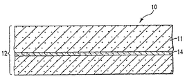


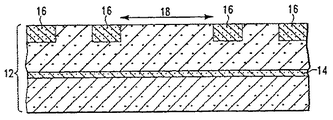
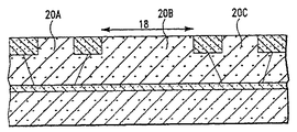
Classifications
-
- H—ELECTRICITY
- H10—SEMICONDUCTOR DEVICES; ELECTRIC SOLID-STATE DEVICES NOT OTHERWISE PROVIDED FOR
- H10D—INORGANIC ELECTRIC SEMICONDUCTOR DEVICES
- H10D1/00—Resistors, capacitors or inductors
- H10D1/60—Capacitors
- H10D1/62—Capacitors having potential barriers
- H10D1/64—Variable-capacitance diodes, e.g. varactors
-
- H—ELECTRICITY
- H10—SEMICONDUCTOR DEVICES; ELECTRIC SOLID-STATE DEVICES NOT OTHERWISE PROVIDED FOR
- H10D—INORGANIC ELECTRIC SEMICONDUCTOR DEVICES
- H10D1/00—Resistors, capacitors or inductors
- H10D1/60—Capacitors
- H10D1/62—Capacitors having potential barriers
- H10D1/66—Conductor-insulator-semiconductor capacitors, e.g. MOS capacitors
-
- H—ELECTRICITY
- H10—SEMICONDUCTOR DEVICES; ELECTRIC SOLID-STATE DEVICES NOT OTHERWISE PROVIDED FOR
- H10D—INORGANIC ELECTRIC SEMICONDUCTOR DEVICES
- H10D84/00—Integrated devices formed in or on semiconductor substrates that comprise only semiconducting layers, e.g. on Si wafers or on GaAs-on-Si wafers
Landscapes
- Metal-Oxide And Bipolar Metal-Oxide Semiconductor Integrated Circuits (AREA)
- Element Separation (AREA)
- Semiconductor Integrated Circuits (AREA)
- Insulated Gate Type Field-Effect Transistor (AREA)
Applications Claiming Priority (2)
| Application Number | Priority Date | Filing Date | Title |
|---|---|---|---|
| US10/711,144 US7714412B2 (en) | 2004-08-27 | 2004-08-27 | MOS varactor using isolation well |
| PCT/US2005/027738 WO2006026055A2 (en) | 2004-08-27 | 2005-08-05 | Mos varactor using isolation well |
Publications (2)
| Publication Number | Publication Date |
|---|---|
| JP2008511989A true JP2008511989A (ja) | 2008-04-17 |
| JP2008511989A5 JP2008511989A5 (cg-RX-API-DMAC7.html) | 2008-07-24 |
Family
ID=35941835
Family Applications (1)
| Application Number | Title | Priority Date | Filing Date |
|---|---|---|---|
| JP2007529890A Pending JP2008511989A (ja) | 2004-08-27 | 2005-08-05 | 分離ウェルを用いるmosバラクタ |
Country Status (7)
| Country | Link |
|---|---|
| US (1) | US7714412B2 (cg-RX-API-DMAC7.html) |
| EP (1) | EP1800343A4 (cg-RX-API-DMAC7.html) |
| JP (1) | JP2008511989A (cg-RX-API-DMAC7.html) |
| KR (1) | KR101013251B1 (cg-RX-API-DMAC7.html) |
| CN (1) | CN101015058A (cg-RX-API-DMAC7.html) |
| TW (1) | TWI353654B (cg-RX-API-DMAC7.html) |
| WO (1) | WO2006026055A2 (cg-RX-API-DMAC7.html) |
Families Citing this family (19)
| Publication number | Priority date | Publication date | Assignee | Title |
|---|---|---|---|---|
| US20070013026A1 (en) * | 2005-07-12 | 2007-01-18 | Ching-Hung Kao | Varactor structure and method for fabricating the same |
| US7936041B2 (en) | 2006-09-15 | 2011-05-03 | International Business Machines Corporation | Schottky barrier diodes for millimeter wave SiGe BICMOS applications |
| US20080149983A1 (en) * | 2006-12-20 | 2008-06-26 | International Business Machines Corporation | Metal-oxide-semiconductor (mos) varactors and methods of forming mos varactors |
| US7598560B2 (en) * | 2007-03-30 | 2009-10-06 | Kavalieros Jack T | Hetero-bimos injection process for non-volatile flash memory |
| EP2420958B1 (en) * | 2008-04-07 | 2016-10-19 | Ruizhang Technology Limited Company | Voltage multiplier powering RFID tags |
| US7804119B2 (en) * | 2008-04-08 | 2010-09-28 | International Business Machines Corporation | Device structures with a hyper-abrupt P-N junction, methods of forming a hyper-abrupt P-N junction, and design structures for an integrated circuit |
| CN101924142B (zh) * | 2009-06-17 | 2011-09-14 | 中国科学院微电子研究所 | 一种GaAs肖特基变容二极管及其制作方法 |
| TWI513011B (zh) * | 2011-07-06 | 2015-12-11 | United Microelectronics Corp | 差動可變電容元件 |
| US9236466B1 (en) | 2011-10-07 | 2016-01-12 | Mie Fujitsu Semiconductor Limited | Analog circuits having improved insulated gate transistors, and methods therefor |
| JP2013143446A (ja) * | 2012-01-10 | 2013-07-22 | Sony Corp | 容量素子、半導体装置及び電子機器 |
| US8586439B1 (en) | 2012-07-11 | 2013-11-19 | International Business Machines Corporation | Inversion mode varactor |
| CN106485290B (zh) | 2015-08-24 | 2019-08-13 | 瑞章科技有限公司 | 增强标签反向散射能量的装置及方法 |
| KR102345676B1 (ko) * | 2015-09-09 | 2021-12-31 | 에스케이하이닉스 주식회사 | 모스 버렉터 및 이를 포함하는 반도체 집적소자 |
| US9960284B2 (en) | 2015-10-30 | 2018-05-01 | Globalfoundries Inc. | Semiconductor structure including a varactor |
| US9882066B1 (en) | 2017-02-10 | 2018-01-30 | Qualcomm Incorporated | Transcap manufacturing techniques without a silicide-blocking mask |
| US10840387B2 (en) * | 2018-04-05 | 2020-11-17 | Qualcomm Incorporated | Buried oxide transcap devices |
| US10622491B2 (en) | 2018-06-21 | 2020-04-14 | Qualcomm Incorporated | Well doping for metal oxide semiconductor (MOS) varactor |
| US10958216B2 (en) | 2019-08-22 | 2021-03-23 | Taiwan Semiconductor Manufacturing Co., Ltd. | Semiconductor device and operation method thereof |
| US20230420578A1 (en) * | 2022-06-24 | 2023-12-28 | Intel Corporation | Varactor device with backside electrical contact |
Citations (5)
| Publication number | Priority date | Publication date | Assignee | Title |
|---|---|---|---|---|
| JP2001177059A (ja) * | 1999-11-12 | 2001-06-29 | Motorola Inc | Cmos工程におけるリニア・コンデンサ構造 |
| US20020074589A1 (en) * | 2000-11-28 | 2002-06-20 | Kamel Benaissa | Semiconductor varactor with reduced parasitic resistance |
| JP2003068869A (ja) * | 2001-08-24 | 2003-03-07 | Mitsubishi Electric Corp | 半導体装置及びその製造方法 |
| JP2004235577A (ja) * | 2003-01-31 | 2004-08-19 | Nec Electronics Corp | 電圧制御可変容量素子 |
| JP2005079159A (ja) * | 2003-08-28 | 2005-03-24 | Matsushita Electric Ind Co Ltd | 半導体装置及びその製造方法 |
Family Cites Families (17)
| Publication number | Priority date | Publication date | Assignee | Title |
|---|---|---|---|---|
| US5742090A (en) * | 1996-04-04 | 1998-04-21 | Advanced Micro Devices, Inc. | Narrow width trenches for field isolation in integrated circuits |
| EP1981087B1 (en) | 1997-09-11 | 2012-11-21 | TELEFONAKTIEBOLAGET LM ERICSSON (publ) | Electrical device comprising a voltage dependant capacitance and method for manufacturing the same |
| US6172378B1 (en) * | 1999-05-03 | 2001-01-09 | Silicon Wave, Inc. | Integrated circuit varactor having a wide capacitance range |
| US6566971B1 (en) * | 2000-02-24 | 2003-05-20 | Broadcom Corporation | Method and circuitry for implementing a differentially tuned varactor-inductor oscillator |
| US6407412B1 (en) * | 2000-03-10 | 2002-06-18 | Pmc-Sierra Inc. | MOS varactor structure with engineered voltage control range |
| US6917095B1 (en) * | 2000-05-30 | 2005-07-12 | Altera Corporation | Integrated radio frequency circuits |
| US6521939B1 (en) * | 2000-09-29 | 2003-02-18 | Chartered Semiconductor Manufacturing Ltd. | High performance integrated varactor on silicon |
| KR100425578B1 (ko) * | 2001-09-17 | 2004-04-03 | 한국전자통신연구원 | SiGe 이종접합 바이폴라 트랜지스터를 이용하여개선된 Q-인자 특성을 갖는 버렉터 및 그 제조 방법 |
| US6542043B1 (en) * | 2001-10-16 | 2003-04-01 | Broadcom Corporation | All PMOS fully differential voltage controlled oscillator |
| SE520590C2 (sv) | 2001-11-15 | 2003-07-29 | Ericsson Telefon Ab L M | Halvledarprocess och PMOS-varaktor |
| US6521506B1 (en) * | 2001-12-13 | 2003-02-18 | International Business Machines Corporation | Varactors for CMOS and BiCMOS technologies |
| US6670654B2 (en) * | 2002-01-09 | 2003-12-30 | International Business Machines Corporation | Silicon germanium heterojunction bipolar transistor with carbon incorporation |
| JP3877597B2 (ja) * | 2002-01-21 | 2007-02-07 | シャープ株式会社 | マルチ端子型mosバラクタ |
| US6608362B1 (en) * | 2002-08-20 | 2003-08-19 | Chartered Semiconductor Manufacturing Ltd. | Method and device for reducing capacitive and magnetic effects from a substrate by using a schottky diode under passive components |
| TW575989B (en) * | 2002-09-25 | 2004-02-11 | Mediatek Inc | NPN Darlington ESD protection circuit |
| US6847095B2 (en) * | 2003-04-01 | 2005-01-25 | Texas Instruments Incorporated | Variable reactor (varactor) with engineered capacitance-voltage characteristics |
| US6949440B2 (en) * | 2003-11-11 | 2005-09-27 | United Microelectronics Corp. | Method of forming a varactor |
-
2004
- 2004-08-27 US US10/711,144 patent/US7714412B2/en not_active Expired - Lifetime
-
2005
- 2005-08-02 TW TW094126260A patent/TWI353654B/zh not_active IP Right Cessation
- 2005-08-05 EP EP05782737A patent/EP1800343A4/en not_active Withdrawn
- 2005-08-05 CN CNA2005800288291A patent/CN101015058A/zh active Pending
- 2005-08-05 JP JP2007529890A patent/JP2008511989A/ja active Pending
- 2005-08-05 WO PCT/US2005/027738 patent/WO2006026055A2/en not_active Ceased
- 2005-08-05 KR KR1020077003435A patent/KR101013251B1/ko not_active Expired - Fee Related
Patent Citations (5)
| Publication number | Priority date | Publication date | Assignee | Title |
|---|---|---|---|---|
| JP2001177059A (ja) * | 1999-11-12 | 2001-06-29 | Motorola Inc | Cmos工程におけるリニア・コンデンサ構造 |
| US20020074589A1 (en) * | 2000-11-28 | 2002-06-20 | Kamel Benaissa | Semiconductor varactor with reduced parasitic resistance |
| JP2003068869A (ja) * | 2001-08-24 | 2003-03-07 | Mitsubishi Electric Corp | 半導体装置及びその製造方法 |
| JP2004235577A (ja) * | 2003-01-31 | 2004-08-19 | Nec Electronics Corp | 電圧制御可変容量素子 |
| JP2005079159A (ja) * | 2003-08-28 | 2005-03-24 | Matsushita Electric Ind Co Ltd | 半導体装置及びその製造方法 |
Also Published As
| Publication number | Publication date |
|---|---|
| US20060043454A1 (en) | 2006-03-02 |
| US7714412B2 (en) | 2010-05-11 |
| KR20070053219A (ko) | 2007-05-23 |
| TWI353654B (en) | 2011-12-01 |
| TW200610103A (en) | 2006-03-16 |
| WO2006026055A3 (en) | 2006-12-14 |
| EP1800343A4 (en) | 2008-11-19 |
| KR101013251B1 (ko) | 2011-02-09 |
| CN101015058A (zh) | 2007-08-08 |
| WO2006026055A2 (en) | 2006-03-09 |
| EP1800343A2 (en) | 2007-06-27 |
Similar Documents
| Publication | Publication Date | Title |
|---|---|---|
| CN101179074B (zh) | 集成半导体器件及其形成方法 | |
| KR101013251B1 (ko) | 분리 웰을 이용한 mos 버랙터 | |
| US6521506B1 (en) | Varactors for CMOS and BiCMOS technologies | |
| US6475838B1 (en) | Methods for forming decoupling capacitors | |
| US6521939B1 (en) | High performance integrated varactor on silicon | |
| US6630377B1 (en) | Method for making high-gain vertical bipolar junction transistor structures compatible with CMOS process | |
| CN101030604B (zh) | 半导体结构及其制造方法 | |
| CN102738246B (zh) | 具有金属栅电极的肖特基二极管及其形成方法 | |
| US20070232010A1 (en) | Method for fabricating a junction varactor with high q factor | |
| KR20030095402A (ko) | 실리콘 온 인슐레이터 전계 효과 트랜지스터(soifet) 및 그의 제조 방법 | |
| JP5044818B2 (ja) | 補償されたカソード・コンタクトを使用する1マスク超階段接合バラクタの形成方法 | |
| JPWO2004097943A1 (ja) | 半導体装置とその製造方法 | |
| US20090039461A1 (en) | Formation of improved soi substrates using bulk semiconductor wafers | |
| US20090065817A1 (en) | Dielectric spacer removal | |
| US20080149983A1 (en) | Metal-oxide-semiconductor (mos) varactors and methods of forming mos varactors | |
| US7682919B2 (en) | Semiconductor process and PMOS varactor | |
| US20050035412A1 (en) | Semiconductor fabrication process, lateral PNP transistor, and integrated circuit | |
| KR20040000442A (ko) | 반도체 디바이스 제조 방법 및 바이폴라 트랜지스터 | |
| US9748270B2 (en) | Tunable capacitor for FDSOI applications | |
| US7554174B2 (en) | Bipolar transistor having semiconductor patterns filling contact windows of an insulating layer | |
| JP2008500720A (ja) | 半導体装置及びそのような装置を製造する方法 | |
| US7491632B2 (en) | Buried subcollector for high frequency passive semiconductor devices | |
| JP2001189321A (ja) | 横型ヘテロバイポーラトランジスタ及びその製造方法 | |
| JP2003218364A (ja) | 半導体装置およびその製造方法 |
Legal Events
| Date | Code | Title | Description |
|---|---|---|---|
| A521 | Request for written amendment filed |
Free format text: JAPANESE INTERMEDIATE CODE: A523 Effective date: 20080530 |
|
| A621 | Written request for application examination |
Free format text: JAPANESE INTERMEDIATE CODE: A621 Effective date: 20080530 |
|
| A977 | Report on retrieval |
Free format text: JAPANESE INTERMEDIATE CODE: A971007 Effective date: 20110304 |
|
| A131 | Notification of reasons for refusal |
Free format text: JAPANESE INTERMEDIATE CODE: A131 Effective date: 20110315 |
|
| RD12 | Notification of acceptance of power of sub attorney |
Free format text: JAPANESE INTERMEDIATE CODE: A7432 Effective date: 20110325 |
|
| A521 | Request for written amendment filed |
Free format text: JAPANESE INTERMEDIATE CODE: A821 Effective date: 20110325 |
|
| A521 | Request for written amendment filed |
Free format text: JAPANESE INTERMEDIATE CODE: A523 Effective date: 20110613 |
|
| A02 | Decision of refusal |
Free format text: JAPANESE INTERMEDIATE CODE: A02 Effective date: 20110712 |
|
| RD14 | Notification of resignation of power of sub attorney |
Free format text: JAPANESE INTERMEDIATE CODE: A7434 Effective date: 20110712 |