JP2008511989A - MOS varactor using isolation well - Google Patents
MOS varactor using isolation well Download PDFInfo
- Publication number
- JP2008511989A JP2008511989A JP2007529890A JP2007529890A JP2008511989A JP 2008511989 A JP2008511989 A JP 2008511989A JP 2007529890 A JP2007529890 A JP 2007529890A JP 2007529890 A JP2007529890 A JP 2007529890A JP 2008511989 A JP2008511989 A JP 2008511989A
- Authority
- JP
- Japan
- Prior art keywords
- region
- conductivity type
- well
- well region
- semiconductor substrate
- Prior art date
- Legal status (The legal status is an assumption and is not a legal conclusion. Google has not performed a legal analysis and makes no representation as to the accuracy of the status listed.)
- Pending
Links
- 238000002955 isolation Methods 0.000 title claims abstract description 62
- 239000000758 substrate Substances 0.000 claims abstract description 68
- 239000004065 semiconductor Substances 0.000 claims abstract description 56
- 238000000034 method Methods 0.000 claims abstract description 45
- 239000004020 conductor Substances 0.000 claims abstract description 26
- 230000005669 field effect Effects 0.000 claims abstract description 12
- 238000004519 manufacturing process Methods 0.000 claims abstract description 10
- 239000002019 doping agent Substances 0.000 claims description 41
- 229910021420 polycrystalline silicon Inorganic materials 0.000 claims description 18
- 238000005468 ion implantation Methods 0.000 claims description 16
- 229920005591 polysilicon Polymers 0.000 claims description 14
- 125000006850 spacer group Chemical group 0.000 claims description 9
- 238000000926 separation method Methods 0.000 abstract description 2
- 125000004429 atom Chemical group 0.000 description 26
- 238000000137 annealing Methods 0.000 description 15
- 238000002513 implantation Methods 0.000 description 10
- 238000005530 etching Methods 0.000 description 9
- 238000003860 storage Methods 0.000 description 9
- 239000007943 implant Substances 0.000 description 8
- 238000005137 deposition process Methods 0.000 description 6
- 229920002120 photoresistant polymer Polymers 0.000 description 6
- 238000005516 engineering process Methods 0.000 description 5
- 229910000577 Silicon-germanium Inorganic materials 0.000 description 4
- 230000015572 biosynthetic process Effects 0.000 description 4
- 238000005229 chemical vapour deposition Methods 0.000 description 4
- 238000000151 deposition Methods 0.000 description 4
- 230000008021 deposition Effects 0.000 description 4
- 239000012212 insulator Substances 0.000 description 4
- 150000004767 nitrides Chemical class 0.000 description 4
- 230000003647 oxidation Effects 0.000 description 4
- 238000007254 oxidation reaction Methods 0.000 description 4
- XUIMIQQOPSSXEZ-UHFFFAOYSA-N Silicon Chemical compound [Si] XUIMIQQOPSSXEZ-UHFFFAOYSA-N 0.000 description 3
- 229910052785 arsenic Inorganic materials 0.000 description 3
- 230000001413 cellular effect Effects 0.000 description 3
- 150000002500 ions Chemical class 0.000 description 3
- 238000001459 lithography Methods 0.000 description 3
- 239000002184 metal Substances 0.000 description 3
- 229910052751 metal Inorganic materials 0.000 description 3
- 230000003071 parasitic effect Effects 0.000 description 3
- 229910052698 phosphorus Inorganic materials 0.000 description 3
- 229910052710 silicon Inorganic materials 0.000 description 3
- 239000010703 silicon Substances 0.000 description 3
- 229910004298 SiO 2 Inorganic materials 0.000 description 2
- BOTDANWDWHJENH-UHFFFAOYSA-N Tetraethyl orthosilicate Chemical compound CCO[Si](OCC)(OCC)OCC BOTDANWDWHJENH-UHFFFAOYSA-N 0.000 description 2
- 230000004913 activation Effects 0.000 description 2
- 238000000231 atomic layer deposition Methods 0.000 description 2
- 229910052796 boron Inorganic materials 0.000 description 2
- 239000003990 capacitor Substances 0.000 description 2
- 238000009792 diffusion process Methods 0.000 description 2
- 238000001312 dry etching Methods 0.000 description 2
- 238000011049 filling Methods 0.000 description 2
- 229910052733 gallium Inorganic materials 0.000 description 2
- 229910052738 indium Inorganic materials 0.000 description 2
- 239000000463 material Substances 0.000 description 2
- 239000000203 mixture Substances 0.000 description 2
- 230000000737 periodic effect Effects 0.000 description 2
- 238000005240 physical vapour deposition Methods 0.000 description 2
- 229910021332 silicide Inorganic materials 0.000 description 2
- FVBUAEGBCNSCDD-UHFFFAOYSA-N silicide(4-) Chemical compound [Si-4] FVBUAEGBCNSCDD-UHFFFAOYSA-N 0.000 description 2
- 239000000126 substance Substances 0.000 description 2
- 230000001360 synchronised effect Effects 0.000 description 2
- 229910018072 Al 2 O 3 Inorganic materials 0.000 description 1
- 229910001218 Gallium arsenide Inorganic materials 0.000 description 1
- 229910000673 Indium arsenide Inorganic materials 0.000 description 1
- 229910021193 La 2 O 3 Inorganic materials 0.000 description 1
- 229910003811 SiGeC Inorganic materials 0.000 description 1
- 229910002367 SrTiO Inorganic materials 0.000 description 1
- 229910010413 TiO 2 Inorganic materials 0.000 description 1
- 229910052782 aluminium Inorganic materials 0.000 description 1
- 229910052787 antimony Inorganic materials 0.000 description 1
- 229910052797 bismuth Inorganic materials 0.000 description 1
- 238000003486 chemical etching Methods 0.000 description 1
- 238000000224 chemical solution deposition Methods 0.000 description 1
- 238000004891 communication Methods 0.000 description 1
- 230000000295 complement effect Effects 0.000 description 1
- 230000003111 delayed effect Effects 0.000 description 1
- 238000000280 densification Methods 0.000 description 1
- 230000000694 effects Effects 0.000 description 1
- 238000001704 evaporation Methods 0.000 description 1
- 230000008020 evaporation Effects 0.000 description 1
- 238000000227 grinding Methods 0.000 description 1
- 125000005843 halogen group Chemical group 0.000 description 1
- 238000011065 in-situ storage Methods 0.000 description 1
- RPQDHPTXJYYUPQ-UHFFFAOYSA-N indium arsenide Chemical compound [In]#[As] RPQDHPTXJYYUPQ-UHFFFAOYSA-N 0.000 description 1
- 238000002347 injection Methods 0.000 description 1
- 239000007924 injection Substances 0.000 description 1
- 239000011810 insulating material Substances 0.000 description 1
- 230000010354 integration Effects 0.000 description 1
- 238000010884 ion-beam technique Methods 0.000 description 1
- 238000000608 laser ablation Methods 0.000 description 1
- 229910052914 metal silicate Inorganic materials 0.000 description 1
- 229910003465 moissanite Inorganic materials 0.000 description 1
- -1 nitride silicates Chemical class 0.000 description 1
- 238000000059 patterning Methods 0.000 description 1
- 238000001020 plasma etching Methods 0.000 description 1
- 238000000623 plasma-assisted chemical vapour deposition Methods 0.000 description 1
- 238000005498 polishing Methods 0.000 description 1
- 230000005855 radiation Effects 0.000 description 1
- 238000005546 reactive sputtering Methods 0.000 description 1
- 150000004760 silicates Chemical class 0.000 description 1
- 229910010271 silicon carbide Inorganic materials 0.000 description 1
- 238000003786 synthesis reaction Methods 0.000 description 1
- 229910052716 thallium Inorganic materials 0.000 description 1
- 238000007740 vapor deposition Methods 0.000 description 1
Images


Classifications
-
- H—ELECTRICITY
- H01—ELECTRIC ELEMENTS
- H01L—SEMICONDUCTOR DEVICES NOT COVERED BY CLASS H10
- H01L29/00—Semiconductor devices adapted for rectifying, amplifying, oscillating or switching, or capacitors or resistors with at least one potential-jump barrier or surface barrier, e.g. PN junction depletion layer or carrier concentration layer; Details of semiconductor bodies or of electrodes thereof ; Multistep manufacturing processes therefor
- H01L29/66—Types of semiconductor device ; Multistep manufacturing processes therefor
- H01L29/86—Types of semiconductor device ; Multistep manufacturing processes therefor controllable only by variation of the electric current supplied, or only the electric potential applied, to one or more of the electrodes carrying the current to be rectified, amplified, oscillated or switched
- H01L29/92—Capacitors with potential-jump barrier or surface barrier
- H01L29/93—Variable capacitance diodes, e.g. varactors
-
- H—ELECTRICITY
- H01—ELECTRIC ELEMENTS
- H01L—SEMICONDUCTOR DEVICES NOT COVERED BY CLASS H10
- H01L27/00—Devices consisting of a plurality of semiconductor or other solid-state components formed in or on a common substrate
- H01L27/02—Devices consisting of a plurality of semiconductor or other solid-state components formed in or on a common substrate including semiconductor components specially adapted for rectifying, oscillating, amplifying or switching and having at least one potential-jump barrier or surface barrier; including integrated passive circuit elements with at least one potential-jump barrier or surface barrier
- H01L27/04—Devices consisting of a plurality of semiconductor or other solid-state components formed in or on a common substrate including semiconductor components specially adapted for rectifying, oscillating, amplifying or switching and having at least one potential-jump barrier or surface barrier; including integrated passive circuit elements with at least one potential-jump barrier or surface barrier the substrate being a semiconductor body
-
- H—ELECTRICITY
- H01—ELECTRIC ELEMENTS
- H01L—SEMICONDUCTOR DEVICES NOT COVERED BY CLASS H10
- H01L29/00—Semiconductor devices adapted for rectifying, amplifying, oscillating or switching, or capacitors or resistors with at least one potential-jump barrier or surface barrier, e.g. PN junction depletion layer or carrier concentration layer; Details of semiconductor bodies or of electrodes thereof ; Multistep manufacturing processes therefor
- H01L29/66—Types of semiconductor device ; Multistep manufacturing processes therefor
- H01L29/86—Types of semiconductor device ; Multistep manufacturing processes therefor controllable only by variation of the electric current supplied, or only the electric potential applied, to one or more of the electrodes carrying the current to be rectified, amplified, oscillated or switched
- H01L29/92—Capacitors with potential-jump barrier or surface barrier
- H01L29/94—Metal-insulator-semiconductors, e.g. MOS
Abstract
【課題】 向上した調節能力と高い品質係数Qとを有するバラクタ及びその製造方法を提供すること。
【解決手段】 本発明は、向上した調節能力と高い品質係数Qとを有するバラクタ22、及び、バラクタ22を製造する方法を提供する。本発明の方法は、従来のCMOS処理スキーム又はBiCMOS処理スキームに組み込むことができる。この方法は、第1の導電型の半導体基板12と、該基板12の上部領域11の下方に配置された、第2の導電型のサブコレクタ14又は分離ウェル(すなわち、ドープ領域)とを含む構造体であって、該第1の導電型は、第2の導電型とは異なる構造体を準備するステップを含む。次に、複数の分離領域16が、基板12の上部領域11内に形成され、次いで、ウェル領域が、基板12の上部領域11内に形成される。場合によっては、本発明のプロセスのこの時点で、ドープ領域14が形成される。ウェル領域は、第2の導電型の外側ウェル領域20A及び20Cと、第1の導電型の内側ウェル領域20Bとを含む。ウェル領域の各々のウェルは、分離領域16によって上面で分離される。次に、内側ウェル領域20Bの上方に、少なくとも第1の導電型のゲート導体26を有する電界効果トランジスタが形成される。
【選択図】 図4PROBLEM TO BE SOLVED: To provide a varactor having improved adjusting ability and a high quality factor Q and a method for manufacturing the varactor.
The present invention provides a varactor 22 having improved adjustability and a high quality factor Q, and a method of manufacturing the varactor 22. The method of the present invention can be incorporated into conventional CMOS processing schemes or BiCMOS processing schemes. The method includes a semiconductor substrate 12 of a first conductivity type and a sub-collector 14 or isolation well (ie, a doped region) of a second conductivity type disposed below the upper region 11 of the substrate 12. A structure, wherein the first conductivity type includes providing a structure different from the second conductivity type. Next, a plurality of isolation regions 16 are formed in the upper region 11 of the substrate 12, and then a well region is formed in the upper region 11 of the substrate 12. In some cases, a doped region 14 is formed at this point in the process of the present invention. The well region includes the second conductivity type outer well regions 20A and 20C and the first conductivity type inner well region 20B. Each well of the well region is separated on the upper surface by the separation region 16. Next, a field effect transistor having at least the first conductivity type gate conductor 26 is formed above the inner well region 20B.
[Selection] Figure 4
Description
本発明は、場合によっては、負のバイアスをかけることを可能にする改善された調節能力と、例えば、寄生(parasitics)のような、雑音を低減させる分離領域とを有するバラクタを含む相補型金属酸化膜半導体(CMOS)及びバイポーラ/CMOS(BiCMOS)電子デバイス、並びに、こうしたデバイスを製造する方法に関する。バラクタを含む本発明の電子デバイスは、携帯電話又はセルラ式電話、携帯用情報端末(PDA)及び他の高RF(無線周波数)電子デバイスに用いるのに非常に適している。 The present invention is a complementary metal comprising a varactor having an improved adjustment capability that in some cases can be negatively biased and an isolation region that reduces noise, eg, parasitics. The present invention relates to oxide semiconductor (CMOS) and bipolar / CMOS (BiCMOS) electronic devices and methods of manufacturing such devices. The electronic device of the present invention including a varactor is very suitable for use in mobile or cellular telephones, personal digital assistants (PDAs) and other high RF (radio frequency) electronic devices.
バラクタは、適切な電圧又は電流バイアスによって制御される静電容量を有する電子デバイスである。バラクタは、一般に、例えば、発振器の周波数が適用される電流又は電圧によって制御される、いわゆる電圧制御発振器(voltage controlled oscillator、VCO)において用いられる。こうした場合には、可変周波数が必要とされるとき、又は、信号を基準信号に同期させる必要があるとき、VCOが用いられる。 A varactor is an electronic device having a capacitance that is controlled by an appropriate voltage or current bias. Varactors are typically used in so-called voltage controlled oscillators (VCOs), for example, where the frequency of the oscillator is controlled by the applied current or voltage. In such cases, a VCO is used when a variable frequency is needed or when the signal needs to be synchronized to a reference signal.
携帯電話/セルラ式電話のような無線通信装置においては、一般に、VCOが、位相ロック・ループ回路において用いられ、無線受信機によって受信される信号と同期される基準信号の生成、変調/復調操作及び周波数合成を含む、適切な信号を生成する。 In wireless communication devices such as cellular / cellular phones, a VCO is typically used in a phase-locked loop circuit to generate, modulate / demodulate a reference signal that is synchronized with the signal received by the wireless receiver. And generate appropriate signals, including frequency synthesis.
多数のバラクタが開発され、集積回路技術において成功裏に用いられている。例えば、バイポーラ、CMOS及びBiCMOS技術においては、バラクタとしてpnダイオード、Schottkyダイオード、又はMOSダイオードを用いることが周知である。非特許文献1においては、pnダイオードを含むバラクタが記載されている。Foxhall他に付与された特許文献1、Goodwin他に付与された特許文献2、Pavlidis他に付与された特許文献3及びNguyen他に付与された特許文献4は、超階段型イオン注入接合領域を含む、他のタイプの可変キャパシタ(すなわち、バラクタ)ダイオードについて記載する。「超階段型」という用語は、注入領域が、隣接する外部ベース領域の壁と接触状態にあるドーピング・プロファイルを有することを示す。他方、Embree他に付与された特許文献5、Stolfa他に付与された特許文献6及びLitwin他に付与された特許文献7は、バラクタとして用いられるMOSダイオードについて記載する。 A number of varactors have been developed and successfully used in integrated circuit technology. For example, in bipolar, CMOS and BiCMOS technologies, it is well known to use pn diodes, Schottky diodes, or MOS diodes as varactors. Non-Patent Document 1 describes a varactor including a pn diode. Patent document 1 granted to Foxhall et al., Patent document 2 granted to Goodwin et al., Patent document 3 granted to Pavlidis et al. And patent document 4 granted to Nguyen et al. Include a super staircase type ion implantation junction region. Other types of variable capacitor (ie, varactor) diodes are described. The term “super-staircase” indicates that the implantation region has a doping profile that is in contact with the wall of the adjacent external base region. On the other hand, Patent Document 5 given to Embree et al., Patent Document 6 given to Stolfa et al. And Patent Document 7 given to Litwin et al. Describe MOS diodes used as varactors.
バラクタの統合は、集積回路技術の能力によって決まる。BiCMOS技術における高RF用途のための集積回路デバイスの概要が、例えば、非特許文献2に記載されている。そこで述べられているように、バラクタは、標準的なBiCMOSデバイス・セットの一部ではない。代わりに、バイポーラ・トランジスタのベース・コレクタ接合をバラクタとして用いることが提案されている。 Varactor integration depends on the capabilities of the integrated circuit technology. An overview of integrated circuit devices for high RF applications in BiCMOS technology is described, for example, in Non-Patent Document 2. As stated there, the varactor is not part of the standard BiCMOS device set. Instead, it has been proposed to use the base-collector junction of a bipolar transistor as a varactor.
デバイスをバラクタとして用いるために、デバイスは、次の基準、すなわち(1)調節能力(すなわち、最大静電容量の最小静電容量に対する比)が大きくなければならない(約3又はそれより大きいオーダー)、(2)品質係数Qが高くなければならない(約20又はそれ以上のオーダー)及び(3)デバイスが直線性を示さなければならない、のうちの1つ又は複数、好ましくは2つ又はそれ以上を満たさなければならない。 In order to use the device as a varactor, the device must have a large (on the order of about 3 or more) the following criteria: (1) adjustment capability (ie, the ratio of maximum capacitance to minimum capacitance) One or more, preferably two or more of (2) the quality factor Q must be high (on the order of about 20 or more) and (3) the device must exhibit linearity Must be met.
知られている従来技術のバラクタの中の多くは、上記の基準を満たしていない。例えば、これまでのベース・コレクタ接合バラクタは、NPNベース・コレクタ・プロファイルに依存しており、バラクタの調節能力のために最適化されていない。注入領域のドーピング・プロファイルが、外部ベース領域の「壁」に配置された超階段型ベース・コレクタ接合バラクタの場合には、デバイスは直線性を欠いている。従来のMOSバラクタを用いる場合、調節能力は高いが、多くの場合、さらに高い調節能力が必要とされる。 Many of the known prior art varactors do not meet the above criteria. For example, previous base-collector junction varactors rely on the NPN base-collector profile and are not optimized for the varactor's adjustability. The device lacks linearity when the doping profile of the implantation region is a super-stepped base-collector junction varactor located on the “wall” of the outer base region. When a conventional MOS varactor is used, the adjustment capability is high, but in many cases, a higher adjustment capability is required.
従来技術のバラクタに関する上述の欠点に鑑みて、上記の基準を満たし、CMOS及びBiCMOSデバイスと統合することができる、新しい改善されたバラクタを提供するための必要性が引き続き存在する。 In view of the above-mentioned drawbacks associated with prior art varactors, there continues to be a need to provide new and improved varactors that meet the above criteria and can be integrated with CMOS and BiCMOS devices.
さらに、従来のMOSバラクタ設計においては、MOSバラクタをバルク基板から電気的に絶縁することは困難である。十分に電気的に絶縁されていないことにより、例えば、雑音のような高い寄生を有するデバイスがもたらされる。したがって、十分に電気的に絶縁され、これによりデバイスの雑音が低減されるバラクタ設計を提供する必要も存在する。 Furthermore, in conventional MOS varactor designs, it is difficult to electrically insulate the MOS varactor from the bulk substrate. Insufficient electrical isolation results in devices with high parasitics such as noise. Therefore, there is also a need to provide a varactor design that is sufficiently electrically isolated, thereby reducing device noise.
本発明は、向上した調節能力と高い品質係数Qとを有するバラクタ、及び、バラクタを製造する方法を提供する。本発明の方法は、従来のCMOS処理スキーム又はBiCMOS処理スキームに組み込むことができる。 The present invention provides a varactor having improved adjustment capability and a high quality factor Q, and a method of manufacturing the varactor. The method of the present invention can be incorporated into conventional CMOS processing schemes or BiCMOS processing schemes.
具体的かつ大まかに言うと、本発明のバラクタは、
第1の導電型の半導体基板であって、この半導体基板は、該半導体基板の上部領域の下方に配置された第2の導電型のドープ領域を含み、第1の導電型は、ドーパント型に関して、第2の導電型とは異なる、第1の導電型の半導体基板と、
前記半導体基板の上部領域内に配置されたウェル領域であって、このウェル領域は、第2の導電型の外側ウェル領域と、第1の導電型の内側ウェル領域とを含み、ウェル領域のウェルの各々は、分離領域によって上面で分離される、ウェル領域と、
内側ウェル領域の上方に配置された、少なくとも第1の導電型のゲート導体を有する電界効果トランジスタと、
を含む。
Specifically and roughly speaking, the varactor of the present invention is
A semiconductor substrate of a first conductivity type, the semiconductor substrate including a doped region of a second conductivity type disposed below an upper region of the semiconductor substrate, wherein the first conductivity type relates to a dopant type A semiconductor substrate of a first conductivity type different from the second conductivity type;
A well region disposed in an upper region of the semiconductor substrate, the well region including a second conductivity type outer well region and a first conductivity type inner well region; Each of which is separated at the upper surface by an isolation region; and a well region;
A field effect transistor having a gate conductor of at least a first conductivity type disposed above the inner well region;
including.
BiCMOS又はバイポーラ・トランジスタが製造される幾つかの実施形態においては、第2の導電型のドープ領域は、サブコレクタである。CMOSデバイスが製造される他の実施形態においては、第2の導電型のドープ領域は、分離ウェルである。 In some embodiments where BiCMOS or bipolar transistors are fabricated, the second conductivity type doped region is a subcollector. In other embodiments in which CMOS devices are fabricated, the second conductivity type doped region is an isolation well.
好ましい実施形態を表す本発明の1つの実施形態において、バラクタは、
半導体基板の上部領域の下方に配置された、n−ドープ領域すなわちサブコレクタ又は分離ウェルを含むp−型半導体基板と、
前記半導体基板の上部領域内に配置されたウェル領域であって、このウェル領域は、外側N−ウェル領域及び内側P−ウェル領域を含み、ウェル領域のウェルの各々は、分離領域によって上面で分離される、ウェル領域と、
内側P−ウェル領域の上方に配置された、少なくともp−型ゲート導体を有する電界効果トランジスタと
を含む。
In one embodiment of the invention representing the preferred embodiment, the varactor is
A p-type semiconductor substrate including an n-doped region, i.e., a subcollector or isolation well, disposed below an upper region of the semiconductor substrate;
A well region disposed in an upper region of the semiconductor substrate, the well region including an outer N-well region and an inner P-well region, and each well of the well region is separated on an upper surface by an isolation region; A well region,
And a field effect transistor having at least a p-type gate conductor disposed above the inner P-well region.
本発明の別の実施形態においては、バラクタは、
半導体基板の上部領域の下方に配置された、p−ドープ領域すなわちサブコレクタ又は分離ウェルを含むn−型半導体基板と、
前記半導体基板の上部領域内に配置されたウェル領域であって、このウェル領域は、外側P−ウェル領域及び内側N−ウェル領域を含み、ウェル領域のウェルの各々は、分離領域によって上面で分離される、ウェル領域と、
内側N−ウェル領域の上方に配置された、少なくともp−型ゲート導体を有する電界効果トランジスタと
を含む。
In another embodiment of the invention, the varactor is
An n-type semiconductor substrate including a p-doped region, i.e., a subcollector or isolation well, disposed below the upper region of the semiconductor substrate;
A well region disposed in an upper region of the semiconductor substrate, the well region including an outer P-well region and an inner N-well region, and each well of the well region is separated on an upper surface by an isolation region; A well region,
And a field effect transistor having at least a p-type gate conductor disposed above the inner N-well region.
バラクタ構造体に加えて、本発明はまた、これを製造する方法も提供する。本方法は、
第1の導電型の半導体基板を含む構造体を準備するステップと、
前記半導体基板の上部領域内に複数の分離領域を形成するステップと、
前記半導体基板の上部領域内にウェル領域を形成するステップであって、このウェル領域は、第1の導電型とは異なる第2の導電型の外側ウェル領域と、第1の導電型の内側ウェル領域とを含み、ウェル領域のウェルの各々は、分離領域によって上面で分離される、ステップと、
内側ウェル領域の上方に、少なくとも第1の導電型のゲート導体を有する電界効果トランジスタを形成するステップと
を含む。
In addition to the varactor structure, the present invention also provides a method of manufacturing it. This method
Providing a structure including a semiconductor substrate of a first conductivity type;
Forming a plurality of isolation regions in an upper region of the semiconductor substrate;
Forming a well region in an upper region of the semiconductor substrate, the well region comprising: an outer well region of a second conductivity type different from the first conductivity type; and an inner well of a first conductivity type. Each of the wells in the well region is separated on the top surface by an isolation region; and
Forming a field effect transistor having a gate conductor of at least a first conductivity type above the inner well region.
1つの実施形態において、半導体基板は、該半導体基板の上部領域の下方に配置された、第2の導電型のドープ領域を含む。ドープ領域は、複数の分離領域を形成する前、又は複数の分離領域を形成した後であるがウェル領域を形成する前に形成することができる。ドープ領域は、BiCMOS又はバイポーラ・デバイスのためのサブコレクタとすることができ、又は、CMOSデバイスのための分離ウェルとすることができることにも留意される。 In one embodiment, the semiconductor substrate includes a doped region of a second conductivity type disposed below the upper region of the semiconductor substrate. The doped region can be formed before forming the plurality of isolation regions, or after forming the plurality of isolation regions but before forming the well region. It is also noted that the doped region can be a subcollector for BiCMOS or bipolar devices, or can be an isolation well for CMOS devices.
好ましいバラクタ構造体の場合は、本方法は、
p−型半導体基板を含む構造体を準備するステップと、
前記半導体基板の上部領域内に複数の分離領域を形成するステップと、
前記半導体基板の上部領域内にウェル領域を形成するステップであって、このウェル領域は、外側ウェルN−領域及び内側P−ウェル領域を含み、ウェル領域のウェルの各々は、分離領域によって上面で分離される、ステップと、
内側ウェル領域の上方に、少なくともp−型ゲート導体を有する電界効果トランジスタを形成するステップと
を含む。
For the preferred varactor structure, the method
providing a structure including a p-type semiconductor substrate;
Forming a plurality of isolation regions in an upper region of the semiconductor substrate;
Forming a well region in an upper region of the semiconductor substrate, the well region including an outer well N-region and an inner P-well region, wherein each well of the well region is separated from the upper surface by an isolation region; Separated, steps,
Forming a field effect transistor having at least a p-type gate conductor above the inner well region.
1つの実施形態において、半導体基板は、該半導体基板の上部領域の下方に配置された、第2の導電型のドープ領域を含む。ドープ領域は、複数の分離領域を形成する前、又は複数の分離領域を形成した後であるがウェル領域を形成する前に形成することができる。 In one embodiment, the semiconductor substrate includes a doped region of a second conductivity type disposed below the upper region of the semiconductor substrate. The doped region can be formed before forming the plurality of isolation regions, or after forming the plurality of isolation regions but before forming the well region.
ここで、改善された調節能力及び減少した寄生すなわち雑音を有するMOSバラクタ、並びに、その製造方法を提供する本発明が、本出願に添付する図面を参照することによってより詳細に説明される。本出願の図面は、説明の目的のために提供されるものであり、よって縮尺に合わせて描かれていないことが留意される。さらに、図面に示される同じ要素及び対応する要素は、同じ参照符号によって示される。 The present invention, which provides a MOS varactor with improved regulation capability and reduced parasitics or noise, and a method of manufacturing the same, will now be described in more detail with reference to the drawings attached to this application. It is noted that the drawings in this application are provided for illustrative purposes and are therefore not drawn to scale. Moreover, the same and corresponding elements shown in the figures are denoted by the same reference numerals.
以下の説明において、交互するN−ウェル、P−ウェル及びN−ウェル・レイアウトと、n−型サブコレクタとを含む、BiCMOS及びバイポーラ用途のためのPMOSバラクタが説明される。こうした配置が詳細に説明されるが、本発明はさらに、交互するP−ウェル、N−ウェル及びP−ウェル・レイアウトと、p−型サブコレクタとを含む、BiCMOS又はバイポーラ用途のためのNMOSバラクタも考慮する。NMOSバラクタは、PMOSバラクタとは反対のドーパントの導電性を用いることによって作られる。例えば、図1−図4に示されるようなBiCMOS又はバイポーラ用途の場合は、基板内に存在する第1の導電型のドーパントとは異なる第2の導電型のドープ領域を表すサブコレクタが存在することが留意される。CMOS用途においては、基板内に存在する第1の導電型のドーパントとは異なる第2の導電型のドープ領域を表す分離ウェルが存在する。ドープ領域は、分離領域を形成する前に、又は分離領域を形成した後であるが本発明のウェル領域を形成する前に形成することができる。 In the following description, PMOS varactors for BiCMOS and bipolar applications are described that include alternating N-well, P-well and N-well layouts and n-type subcollectors. Although such an arrangement is described in detail, the present invention further provides an NMOS varactor for BiCMOS or bipolar applications that includes alternating P-well, N-well and P-well layouts and a p-type subcollector. Also consider. An NMOS varactor is made by using the opposite conductivity of the dopant as the PMOS varactor. For example, for BiCMOS or bipolar applications as shown in FIGS. 1-4, there is a subcollector representing a doped region of a second conductivity type that is different from the first conductivity type dopant present in the substrate. It is noted that. In CMOS applications, there is an isolation well that represents a doped region of a second conductivity type that is different from the first conductivity type dopant present in the substrate. The doped region can be formed before forming the isolation region or after forming the isolation region but before forming the well region of the present invention.
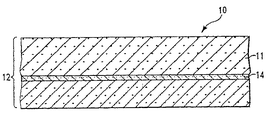
最初に、半導体基板12の一部の中にn+サブコクレタ14が形成された後に形成される初期構造体10を示す図1を参照する。半導体基板12は、例えば、Si、SiGe、SiGeC、SiC、GaAs、InAs、InP、又は例えば、シリコン・オン・インシュレータ(silicon-on-insulator、SOI)、SiGeオン・インシュレータ(SiGe-on-insulator、SGOI)及びSi/SiGe等の層状半導体を含む半導体材料からなる。示される実施形態の場合は、半導体基板12は、p−型基板である。基板12は、基板材料自体、又はn+サブコレクタ14を形成する前に上に形成することができる任意のエピタキシャル成長半導体層を含むことができる上部領域11を含むことに留意されたい。
Reference is first made to FIG. 1 showing the
n+サブコレクタ14は、当業者には公知の通常のイオン注入プロセス及び条件を用いて、As又はPのようなn−型ドーパント原子を注入することによって形成される。注入は、基板全体にわたって連続的なサブコレクタ14を提供するブランケット注入とすることもでき、或いは、マスク・イオン注入プロセスを用いて、基板の特定の部分内に別個のサブコレクタを形成することもできる。用いることができる1つの可能なn−型ドーパントは、約1E14原子/cm2から約5E16原子/cm2までのドーピング用量、及び、約20keVから約100keVまでのエネルギーで注入することができるAsである。上述のもの以外の他のドーパント・イオン及び/又は注入条件を用いることもできる。n+サブコレクタ14は、基板12の上面から、約300nmから約2000nmまでに配置される。
The n +
用いられるドーパントの型にもかかわらず、サブコレクタ14は、一般的には、約1E18原子/cm3から約1E20原子/cm3までのドーパント濃度を有し、約1E19原子/cm3から約1E20原子/cm3までのドーパント濃度がより一般的である。
Regardless of the type of dopant used, the
サブコレクタ14は、本発明のこの時点で形成されるように示されるが、プロセス中、すなわち分離領域の形成後であるがウェル領域の形成前に、サブコレクタ14を後で形成できることに留意されたい。
Although the
上述のような幾つかの実施形態においては、シリコン又はSiGe等のエピタキシャル半導体層が、当業者には公知の従来のエピタキシャル成長プロセスを用いて、半導体基板12の表面上に形成される。こうしたエピタキシャル層は、図1に表記された領域11に対応するものである。
In some embodiments as described above, an epitaxial semiconductor layer such as silicon or SiGe is formed on the surface of the
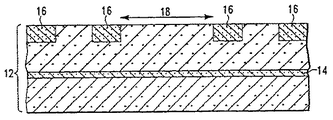
次に、図2に示されるように、複数の分離領域16が、半導体基板12の上部領域11内に形成される。本発明のこの時点で形成される複数の分離領域16は、シリコン局所酸化(local oxidation of silicon、LOCOS)による分離領域とすることができ、或いはより好ましくは、複数の分離領域16は、図2に示されるようなトレンチ分離領域である。分離領域16は、当業者には公知のプロセスを用いて形成される。例えば、分離領域16がLOCOS分離領域からなるとき、こうした分離領域を形成する際に、シリコン局所酸化法を用いることができる。分離領域16がトレンチ分離領域からなるとき、トレンチ分離領域は、リソグラフィ、エッチング及びトレンチ充填(すなわち、テトラエチル・オルトシリケート(TEOS)又は高密度プラズマ酸化物(HDPO)等のトレンチ誘電体の堆積)によって形成される。随意的に、トレンチ充填に続いて、化学機械研磨(CMP)又は研削等の平坦化プロセスを行うことができる。また、任意の緻密化プロセスを用いることもできる。
Next, as shown in FIG. 2, a plurality of
本発明においては、複数の分離領域16が、基板12の上部領域11内に形成され、これらは、n+サブコレクタ14までは延びていない。図2に示されるような2つの分離領域が、デバイス領域18を定める。
In the present invention, a plurality of
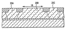
次に、交互する導電性のウェル領域が、イオン注入及びアニールによって形成される。図3に示されるこの例においては、交互する導電性のウェル領域は、第1のN−ウェル領域20A、P−ウェル領域20B及び第2のN−ウェル領域20Cを含む。別の実施形態においては、ウェル領域についての代替的なドーピング構成が形成される。図3に示されるこの例においては、P−ウェル領域(「活性ウェル」)20Bは、デバイス領域18内に配置される。N−ウェル領域20A及び20Cは、デバイス領域18に隣接して形成され、それらのウェル領域は、本明細書においては「リーチ・スルー注入領域」と呼ぶことができる。示されるように、ウェル領域は分離領域16の下方に延びるので、各々の隣接するウェル領域が、例えば、20A及び20Bといった隣接するウェル領域と接触するようになる。図3に示されるように、ウェル領域20A、20B及び20Cは、n+サブコレクタ14の表面まで下方に延びる。サブコレクタ14又は分離ウェル14に電気的に接触させるように、ウェル領域20A及び20Cが用いられる。
Next, alternating conductive well regions are formed by ion implantation and annealing. In this example shown in FIG. 3, the alternating conductive well regions include a first N-
上述のように、ウェル領域は、イオン注入及びアニールによって形成される。各々のウェルを形成するのに用いられるドーパントの型は、最終的なバラクタの極性によって決まる。As及びPのような、元素周期表のVA族からの元素といったn−型ドーパントは、N−ウェルを形成するのに用いられ、B、In及びGaのような元素周期表のIIIA族からの元素といったp−型ドーパントは、P−ウェルを形成するのに用いられる。 As described above, the well region is formed by ion implantation and annealing. The type of dopant used to form each well depends on the polarity of the final varactor. N-type dopants such as elements from group VA of the periodic table, such as As and P, are used to form the N-well, and from group IIIA of the periodic table of elements such as B, In and Ga. A p-type dopant such as an element is used to form a P-well.
用いられるドーパントの型にもかかわらず、各々のウェル領域は、一般的には、約1E17原子/cm3から約1E19原子/cm3までのドーパント濃度を有し、約1E17原子/cm3から約1E18原子/cm3までのドーパント濃度がより一般的である。 Regardless of the type of dopant used, each well region typically has a dopant concentration of about 1E17 atoms / cm 3 to about 1E19 atoms / cm 3 and about 1E17 atoms / cm 3 to about 1E17 atoms / cm 3. A dopant concentration of up to 1E18 atoms / cm 3 is more common.
本発明によると、マスク・イオン注入プロセスを用いて、半導体基板12の一部の中に選択的なドーパント・イオンの型が注入される。同じ注入条件を用いて、外側ウェル領域20A及び20Cを同時に形成することができる。代替的に、異なる注入条件を用いて、異なったときに外側ウェル領域20A及び20Cを形成することもできる。注入の順序は異なり得る。例えば、ウェル領域20A及び20Cの前又は後に、ウェル領域20Bを形成することができる。
In accordance with the present invention, a selective dopant ion type is implanted into a portion of the
各々のウェル領域を形成する際に用いられる注入条件は、従来のものであり、当業者には公知である。例えば、N−ウェル領域を形成するための注入条件は、約1E12原子/cm2から約8E15原子/cm2までのn−型ドーパント用量、及び約30keVから約1000keVまでのエネルギーを含むことができる。P−ウェル領域は、約1E12原子/cm2から約8E13原子/cm2までのp−型ドーパント用量、及び約30keVから約600keVのエネルギーを用いて形成することができる。この技術においてリーチ・スルー(n−型)注入が利用可能な場合には、この注入を標準的なN−ウェル注入に置き換える。一般的に、こうしたリーチ・スルー注入は、ドーパント用量が5E13原子/cm2から5E14原子/cm2までであり、エネルギーが100keVから300keVまでの、Sbのようなn−型ドーパントを含む。 The implantation conditions used in forming each well region are conventional and well known to those skilled in the art. For example, implantation conditions to form the N-well region can include an n-type dopant dose of about 1E12 atoms / cm 2 to about 8E15 atoms / cm 2 and an energy of about 30 keV to about 1000 keV. . The P-well region can be formed using a p-type dopant dose of about 1E12 atoms / cm 2 to about 8E13 atoms / cm 2 and an energy of about 30 keV to about 600 keV. If a reach-through (n-type) implant is available in this technique, it is replaced with a standard N-well implant. Generally, such reach-through implants include n-type dopants such as Sb with dopant doses from 5E13 atoms / cm 2 to 5E14 atoms / cm 2 and energies from 100 keV to 300 keV.
実質的に垂直型イオン注入プロセスを用いて、イオン注入を行うこともでき、或いは代替的に、傾斜イオン注入プロセスを用いることもできる。 The ion implantation can be performed using a substantially vertical ion implantation process, or alternatively, a tilted ion implantation process can be used.
各々のウェル領域内のドーパントを活性化させるために、アニール・プロセスが用いられる。ウェル領域が形成された後に単一のアニール・ステップを用いることができ、或いは代替的に、個々のウェル領域の各々の注入に続いて、アニール・プロセスを行うこともできる。本発明に用いられるアニール温度は、一般的には、約900℃又はそれより高く、約1000℃又はそれより高いアニール温度が、より一般的である。アニール時間は、用いられるアニール・プロセスのタイプによって異なり得る。例えば、一般的に、急速熱アニール(RTA)プロセス、レーザ・アニール、又はスパイク・アニールについては、約5分又はそれより短いアニール時間が用いられ、一方、一般的に、炉アニールについては、約30分又はそれより長いアニール時間が用いられる。 An annealing process is used to activate the dopant in each well region. A single annealing step can be used after the well regions are formed, or alternatively, an annealing process can be performed following each implantation of the individual well regions. The annealing temperatures used in the present invention are typically about 900 ° C. or higher, with annealing temperatures of about 1000 ° C. or higher being more common. The annealing time can vary depending on the type of annealing process used. For example, typically an annealing time of about 5 minutes or less is used for a rapid thermal anneal (RTA) process, laser anneal, or spike anneal, while typically for furnace anneal, about An annealing time of 30 minutes or longer is used.
本発明のプロセス内の別の熱サイクルが実行されるまで、ウェル領域の活性化を遅らせることができることに留意すべきである。例えば、ソース/ドレイン拡散の活性化の際に、ウェル領域を活性化させることができる。全体のプロセスの中で、熱サイクル数を減少させ、よって、コストを削減するので、後の熱プロセスまでウェル領域の活性化を遅らせることは、有利である。 It should be noted that well region activation can be delayed until another thermal cycle within the process of the present invention is performed. For example, the well region can be activated when the source / drain diffusion is activated. It is advantageous to delay the activation of the well region until a later thermal process, since it reduces the number of thermal cycles and thus reduces costs in the overall process.
次に、従来のCMOSプロセスを用いて、図4に示されるバラクタ22を提供する。図4に示されるバラクタ22は、ゲート誘電体24と、ゲート導体26と、少なくともゲート導体26の側壁上に配置された少なくとも1つのスペーサ30と、基板12の上部に配置されたソース/ドレイン領域32(32’)とを含む電界効果トランジスタ(FET)を含むことに留意されたい。バラクタ22は、デバイス領域18内の中間ウェル領域すなわちP−ウェル領域20Bの上に配置される。
Next, the
図4に示されるバラクタ22を形成するのに用い得る1つの従来のCMOSプロセスは、次のステップを含む。すなわち、分離領域が堆積された誘電体からなる場合には、最初に、ゲート誘電体24は、半導体基板12と分離領域16を含む図3に示される構造体の表面全体上に形成される。
One conventional CMOS process that can be used to form the
ゲート誘電体24は、例えば、酸化、窒化、又は酸窒化といった熱成長プロセスによって形成することができる。代替的に、ゲート誘電体24は、例えば、化学気相成長(CVD)、プラズマ強化CVD、原子層堆積(ALD)、蒸着、反応性スパッタリング、化学溶液堆積及び他の同様の堆積プロセスのような堆積プロセスによって形成することができる。上記のプロセスの任意の組み合わせを用いて、ゲート誘電体24を形成することもできる。
The
ゲート誘電体24は、これらに限定されるものではないが、酸化物、窒化物、酸窒化物、及び/又は金属シリケート及び窒化金属シリケートを含むシリケートなどの絶縁材料からなる。1つの実施形態において、ゲート誘電体24は、例えば、SiO2、HfO2、ZrO2、Al2O3、TiO2、La2O3、SrTiO3、LaAlO3、及びこれらの混合物のような酸化物からなることが好ましい。
The
ゲート誘電体24の物理的な厚さは異なり得るが、一般的には、ゲート誘電体24は、約0.5nmから約10nmまでの厚さを有し、約0.5nmから約3nmまでの厚さがより一般的である。
Although the physical thickness of the
ゲート誘電体24を形成した後、例えば、物理気相成長、CVD、又は蒸着等の周知の堆積プロセスを用いて、図4に示されるゲート導体26になるポリシリコン(すなわち、ポリSi)のブランケット層が、ゲート誘電体24上に形成される。ポリシリコンのブランケット層は、ドープされたものであっても、ドープされていないものであってもよい。ドープされたものである場合には、ポリシリコン・ブランケット層を形成するのに、その場(in-situ)ドーピング堆積プロセスを用いることができる。代替的に、堆積、イオン注入及びアニールによって、ドープされたポリSi層を形成することができる。ポリSi層のドーピングが、形成されるゲートの仕事関数をシフトさせる。ドーパント・イオンの説明に役立つ実例は、As、P、B、Sb、Bi、In、Al、Ga、Tl、又はこれらの混合物を含む。図に示される例においては、p−ドープされたポリシリコン・ゲート導体26が形成される。イオン注入についての好ましいドーズ量は、1E14(=1×10¹⁴)原子/cm2から1E16(=1×1016)原子/cm2までであり、或いはより好ましくは、1E15原子/cm2から5E15原子/cm2までである。本発明のこの時点で堆積されたポリシリコン層の厚さすなわち高さは、用いられる堆積プロセスによって異なり得る。一般的には、ポリシリコン層は、約20nmから約180nmまでの垂直厚さを有し、約40nmから約150nmまでの厚さがより一般的である。
After forming the
用いられるドーパントの型にもかかわらず、ゲート導体26は、一般的には、約1E19原子/cm3から1E21原子/cm3までのドーパント濃度を有し、約5E19原子/cm3から5E20原子/cm3までのドーパント濃度がより一般的である。
Regardless of the type of dopant used, the
ポリシリコン・ブランケット層の堆積後、例えば、物理気相成長又は化学気相成長等の堆積プロセスを用いて、ハード・マスクが、ポリシリコン・ブランケット層の上に形成される。ハード・マスクは、酸化物、窒化物、酸窒化物、又はこれらの任意の組み合わせとすることができる。1つの実施形態において、例えば、Si3N4のような窒化物が、ハード・マスクとして用いられる。さらに別の実施形態においては、ハード・マスクは、SiO2のような酸化物である。ハード・マスクの厚さすなわち高さは、約20nmから約180nmまでであり、約30nmから約140nmまでの厚さがより一般的である。 After deposition of the polysilicon blanket layer, a hard mask is formed on the polysilicon blanket layer using, for example, a deposition process such as physical vapor deposition or chemical vapor deposition. The hard mask can be an oxide, nitride, oxynitride, or any combination thereof. In one embodiment, a nitride such as Si 3 N 4 is used as a hard mask. In yet another embodiment, the hard mask is an oxide such as SiO 2. The thickness or height of the hard mask is from about 20 nm to about 180 nm, with a thickness from about 30 nm to about 140 nm being more common.
次に、ポリシリコン・ブランケット層及びハード・マスクが、リソグラフィ及びエッチングによってパターン形成され、少なくとも1つのパターン形成されたゲート・スタックを提供する。パターン形成されたゲート・スタックは、同じ寸法すなわち長さを有することができ、或いは、デバイス性能を向上させるために様々な寸法を有することができる。本発明のこの時点のパターン形成されたゲート・スタックの各々は、ポリSiのゲート導体26と、ハード・マスクとを含む。リソグラフィ・ステップは、フォトレジストをハード・マスクの上面に塗布するステップと、フォトレジストを所望のパターンの放射線に露光させるステップと、従来のレジスト現像液を用いて露光されたフォトレジストを現像するステップとを含む。次に、1つ又は複数のドライ・エッチング・ステップを用いて、フォトレジスト内のパターンが、ハード・マスク及びポリシリコンのブランケット層に転写される。幾つかの実施形態においては、ハード・マスク内にパターンが転写された後に、パターン形成されたフォトレジストを除去することができる。他の実施形態においては、エッチングが完了した後に、パターン形成されたフォトレジストが除去される。
The polysilicon blanket layer and hard mask are then patterned by lithography and etching to provide at least one patterned gate stack. Patterned gate stacks can have the same dimensions or lengths, or can have various dimensions to improve device performance. Each of the patterned gate stacks at this point of the present invention includes a poly-
ハード・マスクは、一般に、ゲートのパターン形成プロセス中又はその後に除去されることが留意される。ハード・マスクは、一般に、最終構造体内には存在しない。図4を参照されたい。 It is noted that the hard mask is generally removed during or after the gate patterning process. A hard mask is generally not present in the final structure. Please refer to FIG.
パターン形成されたゲート・スタックを形成する際に本発明に用いることができる適切な乾式エッチング・プロセスは、これらに限定されるものではないが、反応性イオン・エッチング、イオン・ビーム・エッチング、プラズマ・エッチング、又はレーザ切除を含む。用いられる乾式エッチング・プロセスは、一般に、下にあるゲート誘電体24に対して選択的であり、したがって、こうしたエッチング・ステップは、一般に、ゲート誘電体24を除去するものではない。しかしながら、幾つかの実施形態においては、こうしたエッチング・ステップを用いて、ゲート・スタックによって保護されていないゲート誘電体24の一部を除去することができる。
Suitable dry etching processes that can be used in the present invention in forming a patterned gate stack include, but are not limited to, reactive ion etching, ion beam etching, plasma Including etching or laser ablation. The dry etch process used is generally selective to the
次に、少なくとも1つのスペーサ30が、パターン形成されたゲート・スタックの露光された側壁上に形成される。少なくとも1つのスペーサ30は、酸化物、窒化物、酸窒化物、及び/又はこれらの任意の組み合わせといった絶縁体からなる。少なくとも1つのスペーサ30は、堆積及びエッチングによって形成される。
Next, at least one
少なくとも1つのスペーサ30の幅は、ソース及びドレインのシリサイド・コンタクト(後に形成される)がゲート・スタックの縁部の下に侵入しないように、十分に広いものでなければならない。一般的には、少なくとも1つのスペーサ30が、約15nmから約80nmのまでの底部で測定された幅を有するとき、ソース/ドレイン・シリサイドは、ゲート・スタックの縁部の下に侵入しない。
The width of the at least one
スペーサの形成後、基板12内にソース/ドレイン領域32、32´が形成される。ソース/ドレイン領域32、32´は、イオン注入及びアニール・ステップを用いて形成される。アニール・ステップは、前の注入ステップによって注入されたドーパントを活性化させる働きをする。イオン注入及びアニールについての条件は、当業者には公知である。「ソース/ドレイン領域」という用語は、深いソース/ドレイン拡散領域、任意のハロ注入及びソース/ドレイン拡張領域を含む。
After the formation of the spacer, source /
次に、これまでに除去されていなかった場合には、ゲート誘電体24を選択的に除去する化学エッチング・プロセスを用いて、ゲート誘電体24の露光された部分を除去する。こうしたエッチング・ステップは、半導体基板12の上面、及び、分離領域16の上面で停止する。ゲート誘電体24の露光された部分を除去する際に任意の化学エッチング液を用いることができるが、1つの実施形態においては、希フッ化水素酸(dilute hydrofluoric aid、DHF)が用いられる。
Next, if not previously removed, the exposed portion of the
当業者には公知の従来のソース/ドレイン・シリサイド化プロセス及び金属ゲート・シリサイド化プロセスを用いることによって、本発明のこの時点で、ソース/ドレイン領域32、32´及び随意的にゲート導体24の少なくとも一部をシリサイド化することができる。
By using conventional source / drain silicidation processes and metal gate silicidation processes known to those skilled in the art, at this point of the invention, the source /
図4は、BiCMOS又はバイポーラ用途のための本発明の構造体、すなわち、ウェル・スキーム及び下にあるサブコレクタを含む、基板12の上に配置されたバラクタ22を示すことが留意される。図において、バラクタ22は、p−型ポリシリコン・ゲート導体26、下にあるP−ウェル領域20B、分離領域16によってバラクタから分離される隣接するN−ウェル領域20A及び20C、並びにP−ウェル領域20Bをp−型半導体基板12の本体から分離する下にあるn+サブコレクタ14を含む。反対の極性の型の構造体、すなわち、n−型ポリシリコン・ゲート導体26、下にあるN−ウェル領域20B、分離領域16によってバラクタ構造体から分離される隣接するP−ウェル領域20A及び20C、並びにN−ウェル領域20Bをn−型半導体基板12の本体から分離する下にあるp+サブコレクタ14も考慮される。
It is noted that FIG. 4 shows the structure of the present invention for BiCMOS or bipolar applications, ie, a
空乏状態で作動する負バイアス蓄積バラクタを提供するので、図4に示される構造体は、好ましいものである。 The structure shown in FIG. 4 is preferred because it provides a negative bias storage varactor that operates in a depleted state.
必要に応じて、基板12の表面上に他のバラクタ22を形成できることが留意される。
It is noted that
図5は、N−ウェル内の従来技術のNMOS(曲線1)、P−ウェル内の従来技術のPMOS(曲線2)、並びにウェル・スキーム及び下にあるn+サブコレクタ又は分離ウェルを有する、P−ウェル内の本発明のバラクタPMOS(曲線3)についてのCV特性を示す。本発明のバラクタにおける最小静電容量が減少し、よって、曲線1及び曲線2と比較してデバイスの調節能力が向上されることが、この図面から確認される。こうした最小静電容量の減少は、n−型サブコレクタ又は分離ウェルの僅かなカウンタドープの影響である。このことにより、P−ウェル内の本発明のp−型ドーパントが減少され、よって、最小静電容量が減少される。 FIG. 5 shows a prior art NMOS (curve 1) in an N-well, a prior art PMOS in a P-well (curve 2), and a P having a well scheme and an underlying n + subcollector or isolation well. -Shows the CV characteristics for the inventive varactor PMOS (curve 3) in the well. It can be seen from this figure that the minimum capacitance in the varactor of the present invention is reduced, thus improving the adjustment capability of the device compared to Curve 1 and Curve 2. This reduction in minimum capacitance is the effect of a slight counterdoping of the n-type subcollector or isolation well. This reduces the p-type dopant of the present invention in the P-well and thus reduces the minimum capacitance.
図6−図8は、CMOS用途のためのバラクタを形成するのに用いられる処理ステップを示す。このプロセスは、最初に、基板12の上部領域内に形成された複数の分離領域16を有する半導体基板12を含む、図6に示される構造体を準備することで始まる。複数の分離領域16が、上述のように形成される。示されるように、デバイス領域18は、2つの隣接する分離領域間に形成される。半導体基板12は、第1の導電型のドーパント(n−又はp−型)でドープされる。
6-8 illustrate the processing steps used to form varactors for CMOS applications. This process begins by first providing the structure shown in FIG. 6 that includes a
次に、図6に示される構造体内にp−型又はn−型ドーパントをイオン注入することによって、分離ウェル14(すなわち、第2の導電型のドーパント領域)が形成され、図7に示される構造体を生成する。分離ウェル領域14は、当業者には公知の従来の注入プロセスを用いて形成される。
Next, an isolation well 14 (ie, a dopant region of the second conductivity type) is formed by ion implantation of a p-type or n-type dopant into the structure shown in FIG. 6, and is shown in FIG. Create a structure. The
次に、ウェル領域20A、20B及び20Cが、上述のように形成される。20A及び20Cは、分離ウェル領域14と同じ導電型のドーパントを有するリーチ・スルー注入領域であり、活性ウェル領域20Bは、基板と同じ導電型のドーパントを有することに留意されたい。結果物としての構造体が、図8に示される。
Next, well
図4に示される構造体を提供するために、図8に示される構造体上に、上述のさらなる処理を形成することができる。 To provide the structure shown in FIG. 4, the above-described further processing can be formed on the structure shown in FIG.
本発明は、特に、その好ましい実施形態について示され、説明されたが、当業者であれば、本発明の精神及び範囲から逸脱することなく、形態及び詳細における前述した及び他の変更を加えることができることを理解するであろう。したがって、本発明は、説明され、示された正確な形態及び詳細に限定されるものではなく、添付の特許請求の範囲の精神及び範囲内にあることが意図される。 While the invention has been particularly shown and described with respect to preferred embodiments thereof, those skilled in the art will make the foregoing and other changes in form and detail without departing from the spirit and scope of the invention. You will understand that you can. Accordingly, the present invention is not intended to be limited to the precise forms and details described and shown, but is intended to be within the spirit and scope of the appended claims.
Claims (20)
前記半導体基板の前記上部領域内に配置されたウェル領域であって、前記ウェル領域は、前記第2の導電型の外側ウェル領域と、前記第1の導電型の内側ウェル領域とを含み、前記ウェル領域のウェルの各々は、分離領域によって上面で分離される、ウェル領域と、
前記内側ウェル領域の上方に配置された、少なくとも前記第1の導電型のゲート導体を有する電界効果トランジスタと
を備えるバラクタ構造体。 A semiconductor substrate of a first conductivity type, wherein the semiconductor substrate includes a doped region of a second conductivity type disposed below an upper region of the semiconductor substrate, and the first conductivity type includes the first conductivity type A semiconductor substrate of a first conductivity type different from the conductivity type of 2;
A well region disposed in the upper region of the semiconductor substrate, the well region including an outer well region of the second conductivity type and an inner well region of the first conductivity type; Each of the wells in the well region is separated on the top surface by the isolation region;
A varactor structure comprising: a field effect transistor having a gate conductor of at least the first conductivity type disposed above the inner well region.
前記半導体基板の前記上部領域内に配置されたウェル領域であって、前記ウェル領域は、外側N−ウェル領域及び内側P−ウェル領域を含み、該ウェル領域のウェルの各々は、分離領域によって上面で分離される、ウェル領域と、
前記内側P−ウェル領域の上方に配置された、少なくともp−型ゲート導体を有する電界効果トランジスタと
を備えるバラクタ構造体。 A p-type semiconductor substrate including an n-doped region, disposed below an upper region of the semiconductor substrate;
A well region disposed in the upper region of the semiconductor substrate, wherein the well region includes an outer N-well region and an inner P-well region, and each well of the well region is separated from the upper surface by an isolation region. A well region separated by
A varactor structure comprising a field effect transistor having at least a p-type gate conductor disposed above the inner P-well region.
第1の導電型の半導体基板を含む構造体を準備するステップと、
前記半導体基板の上部領域内に複数の分離領域を形成するステップと、
前記半導体基板の前記上部領域内にウェル領域を形成するステップであって、前記ウェル領域は、前記第1の導電型とは異なる第2の導電型の外側ウェル領域と、該第1の導電型の内側ウェル領域とを含み、前記ウェル領域のウェルの各々は、分離領域によって上面で分離される、ステップと、
前記内側ウェル領域の上方に、少なくとも前記第1の導電型のゲート導体を有する電界効果トランジスタを形成するステップであって、前記第2の導電型のドープ領域は、前記複数の分離領域を形成する前又は直後に、前記半導体基板の上部領域内に形成される、ステップと
を含む方法。 A method of manufacturing a varactor structure,
Providing a structure including a semiconductor substrate of a first conductivity type;
Forming a plurality of isolation regions in an upper region of the semiconductor substrate;
Forming a well region in the upper region of the semiconductor substrate, wherein the well region includes an outer well region of a second conductivity type different from the first conductivity type, and the first conductivity type; An inner well region, wherein each of the wells of the well region is separated on the top surface by an isolation region;
Forming a field effect transistor having at least a gate conductor of the first conductivity type above the inner well region, wherein the doped region of the second conductivity type forms the plurality of isolation regions; Forming in the upper region of the semiconductor substrate before or immediately after.
Applications Claiming Priority (2)
| Application Number | Priority Date | Filing Date | Title |
|---|---|---|---|
| US10/711,144 US7714412B2 (en) | 2004-08-27 | 2004-08-27 | MOS varactor using isolation well |
| PCT/US2005/027738 WO2006026055A2 (en) | 2004-08-27 | 2005-08-05 | Mos varactor using isolation well |
Publications (2)
| Publication Number | Publication Date |
|---|---|
| JP2008511989A true JP2008511989A (en) | 2008-04-17 |
| JP2008511989A5 JP2008511989A5 (en) | 2008-07-24 |
Family
ID=35941835
Family Applications (1)
| Application Number | Title | Priority Date | Filing Date |
|---|---|---|---|
| JP2007529890A Pending JP2008511989A (en) | 2004-08-27 | 2005-08-05 | MOS varactor using isolation well |
Country Status (7)
| Country | Link |
|---|---|
| US (1) | US7714412B2 (en) |
| EP (1) | EP1800343A4 (en) |
| JP (1) | JP2008511989A (en) |
| KR (1) | KR101013251B1 (en) |
| CN (1) | CN101015058A (en) |
| TW (1) | TWI353654B (en) |
| WO (1) | WO2006026055A2 (en) |
Families Citing this family (18)
| Publication number | Priority date | Publication date | Assignee | Title |
|---|---|---|---|---|
| US20070013026A1 (en) * | 2005-07-12 | 2007-01-18 | Ching-Hung Kao | Varactor structure and method for fabricating the same |
| US7936041B2 (en) * | 2006-09-15 | 2011-05-03 | International Business Machines Corporation | Schottky barrier diodes for millimeter wave SiGe BICMOS applications |
| US20080149983A1 (en) * | 2006-12-20 | 2008-06-26 | International Business Machines Corporation | Metal-oxide-semiconductor (mos) varactors and methods of forming mos varactors |
| US7598560B2 (en) * | 2007-03-30 | 2009-10-06 | Kavalieros Jack T | Hetero-bimos injection process for non-volatile flash memory |
| CN103593698B (en) * | 2008-04-07 | 2017-05-03 | 瑞章科技有限公司 | Subset selection of RFID tags using light |
| US7804119B2 (en) * | 2008-04-08 | 2010-09-28 | International Business Machines Corporation | Device structures with a hyper-abrupt P-N junction, methods of forming a hyper-abrupt P-N junction, and design structures for an integrated circuit |
| CN101924142B (en) * | 2009-06-17 | 2011-09-14 | 中国科学院微电子研究所 | GaAs Schottky variable capacitance diode and manufacture method thereof |
| TWI513011B (en) * | 2011-07-06 | 2015-12-11 | United Microelectronics Corp | Differential varactor device |
| US9236466B1 (en) | 2011-10-07 | 2016-01-12 | Mie Fujitsu Semiconductor Limited | Analog circuits having improved insulated gate transistors, and methods therefor |
| JP2013143446A (en) * | 2012-01-10 | 2013-07-22 | Sony Corp | Capacitive element, semiconductor device and electronic apparatus |
| US8586439B1 (en) | 2012-07-11 | 2013-11-19 | International Business Machines Corporation | Inversion mode varactor |
| CN106485290B (en) | 2015-08-24 | 2019-08-13 | 瑞章科技有限公司 | Enhance the device and method of tag backscatter energy |
| KR102345676B1 (en) * | 2015-09-09 | 2021-12-31 | 에스케이하이닉스 주식회사 | MOS varactor and semiconductor integrated device including the same |
| US9960284B2 (en) * | 2015-10-30 | 2018-05-01 | Globalfoundries Inc. | Semiconductor structure including a varactor |
| US9882066B1 (en) | 2017-02-10 | 2018-01-30 | Qualcomm Incorporated | Transcap manufacturing techniques without a silicide-blocking mask |
| US10840387B2 (en) * | 2018-04-05 | 2020-11-17 | Qualcomm Incorporated | Buried oxide transcap devices |
| US10622491B2 (en) | 2018-06-21 | 2020-04-14 | Qualcomm Incorporated | Well doping for metal oxide semiconductor (MOS) varactor |
| US10958216B2 (en) | 2019-08-22 | 2021-03-23 | Taiwan Semiconductor Manufacturing Co., Ltd. | Semiconductor device and operation method thereof |
Citations (5)
| Publication number | Priority date | Publication date | Assignee | Title |
|---|---|---|---|---|
| JP2001177059A (en) * | 1999-11-12 | 2001-06-29 | Motorola Inc | Linear capacitor structure in cmos process |
| US20020074589A1 (en) * | 2000-11-28 | 2002-06-20 | Kamel Benaissa | Semiconductor varactor with reduced parasitic resistance |
| JP2003068869A (en) * | 2001-08-24 | 2003-03-07 | Mitsubishi Electric Corp | Semiconductor device and method of manufacturing the same |
| JP2004235577A (en) * | 2003-01-31 | 2004-08-19 | Nec Electronics Corp | Voltage-controlled variable capacitative element |
| JP2005079159A (en) * | 2003-08-28 | 2005-03-24 | Matsushita Electric Ind Co Ltd | Semiconductor device and its manufacturing method |
Family Cites Families (17)
| Publication number | Priority date | Publication date | Assignee | Title |
|---|---|---|---|---|
| US5742090A (en) * | 1996-04-04 | 1998-04-21 | Advanced Micro Devices, Inc. | Narrow width trenches for field isolation in integrated circuits |
| EP0902483B1 (en) | 1997-09-11 | 2008-11-12 | Telefonaktiebolaget LM Ericsson (publ) | Electrical device comprising a voltage dependant capacitance and method of manufacturing the same |
| US6172378B1 (en) * | 1999-05-03 | 2001-01-09 | Silicon Wave, Inc. | Integrated circuit varactor having a wide capacitance range |
| US6566971B1 (en) * | 2000-02-24 | 2003-05-20 | Broadcom Corporation | Method and circuitry for implementing a differentially tuned varactor-inductor oscillator |
| US6407412B1 (en) * | 2000-03-10 | 2002-06-18 | Pmc-Sierra Inc. | MOS varactor structure with engineered voltage control range |
| US6917095B1 (en) * | 2000-05-30 | 2005-07-12 | Altera Corporation | Integrated radio frequency circuits |
| US6521939B1 (en) * | 2000-09-29 | 2003-02-18 | Chartered Semiconductor Manufacturing Ltd. | High performance integrated varactor on silicon |
| KR100425578B1 (en) * | 2001-09-17 | 2004-04-03 | 한국전자통신연구원 | Varactor having improved Q-factor using SiGe heterojunction bipolar transistor and method for fabricating the same |
| US6542043B1 (en) * | 2001-10-16 | 2003-04-01 | Broadcom Corporation | All PMOS fully differential voltage controlled oscillator |
| SE520590C2 (en) | 2001-11-15 | 2003-07-29 | Ericsson Telefon Ab L M | Semiconductor process and PMOS varactor |
| US6521506B1 (en) * | 2001-12-13 | 2003-02-18 | International Business Machines Corporation | Varactors for CMOS and BiCMOS technologies |
| US6670654B2 (en) * | 2002-01-09 | 2003-12-30 | International Business Machines Corporation | Silicon germanium heterojunction bipolar transistor with carbon incorporation |
| JP3877597B2 (en) * | 2002-01-21 | 2007-02-07 | シャープ株式会社 | Multi-terminal MOS varactor |
| US6608362B1 (en) * | 2002-08-20 | 2003-08-19 | Chartered Semiconductor Manufacturing Ltd. | Method and device for reducing capacitive and magnetic effects from a substrate by using a schottky diode under passive components |
| TW575989B (en) * | 2002-09-25 | 2004-02-11 | Mediatek Inc | NPN Darlington ESD protection circuit |
| US6847095B2 (en) * | 2003-04-01 | 2005-01-25 | Texas Instruments Incorporated | Variable reactor (varactor) with engineered capacitance-voltage characteristics |
| US6949440B2 (en) * | 2003-11-11 | 2005-09-27 | United Microelectronics Corp. | Method of forming a varactor |
-
2004
- 2004-08-27 US US10/711,144 patent/US7714412B2/en active Active
-
2005
- 2005-08-02 TW TW094126260A patent/TWI353654B/en not_active IP Right Cessation
- 2005-08-05 WO PCT/US2005/027738 patent/WO2006026055A2/en active Application Filing
- 2005-08-05 CN CNA2005800288291A patent/CN101015058A/en active Pending
- 2005-08-05 EP EP05782737A patent/EP1800343A4/en not_active Withdrawn
- 2005-08-05 KR KR1020077003435A patent/KR101013251B1/en not_active IP Right Cessation
- 2005-08-05 JP JP2007529890A patent/JP2008511989A/en active Pending
Patent Citations (5)
| Publication number | Priority date | Publication date | Assignee | Title |
|---|---|---|---|---|
| JP2001177059A (en) * | 1999-11-12 | 2001-06-29 | Motorola Inc | Linear capacitor structure in cmos process |
| US20020074589A1 (en) * | 2000-11-28 | 2002-06-20 | Kamel Benaissa | Semiconductor varactor with reduced parasitic resistance |
| JP2003068869A (en) * | 2001-08-24 | 2003-03-07 | Mitsubishi Electric Corp | Semiconductor device and method of manufacturing the same |
| JP2004235577A (en) * | 2003-01-31 | 2004-08-19 | Nec Electronics Corp | Voltage-controlled variable capacitative element |
| JP2005079159A (en) * | 2003-08-28 | 2005-03-24 | Matsushita Electric Ind Co Ltd | Semiconductor device and its manufacturing method |
Also Published As
| Publication number | Publication date |
|---|---|
| US7714412B2 (en) | 2010-05-11 |
| TWI353654B (en) | 2011-12-01 |
| CN101015058A (en) | 2007-08-08 |
| TW200610103A (en) | 2006-03-16 |
| WO2006026055A2 (en) | 2006-03-09 |
| KR20070053219A (en) | 2007-05-23 |
| US20060043454A1 (en) | 2006-03-02 |
| EP1800343A4 (en) | 2008-11-19 |
| EP1800343A2 (en) | 2007-06-27 |
| WO2006026055A3 (en) | 2006-12-14 |
| KR101013251B1 (en) | 2011-02-09 |
Similar Documents
| Publication | Publication Date | Title |
|---|---|---|
| KR101013251B1 (en) | Mos varactor using isolation well | |
| US7705426B2 (en) | Integration of a SiGe- or SiGeC-based HBT with a SiGe- or SiGeC-strapped semiconductor device | |
| JP5044818B2 (en) | Method for forming a one-mask super staircase junction varactor using compensated cathode contact | |
| US7135375B2 (en) | Varactors for CMOS and BiCMOS technologies | |
| US6475838B1 (en) | Methods for forming decoupling capacitors | |
| US6521939B1 (en) | High performance integrated varactor on silicon | |
| US6630377B1 (en) | Method for making high-gain vertical bipolar junction transistor structures compatible with CMOS process | |
| US7560798B2 (en) | High performance tapered varactor | |
| US20080149983A1 (en) | Metal-oxide-semiconductor (mos) varactors and methods of forming mos varactors | |
| KR20030095402A (en) | Soi device with reduced junction capacitance | |
| JPWO2004097943A1 (en) | Semiconductor device and manufacturing method thereof | |
| CN103262246A (en) | Structure and method for Vt tuning and short channel control with high k/metal gate MOSFETS | |
| JPH0567787A (en) | Soi field-effect transistor | |
| US20070232010A1 (en) | Method for fabricating a junction varactor with high q factor | |
| US7919379B2 (en) | Dielectric spacer removal | |
| US7682919B2 (en) | Semiconductor process and PMOS varactor | |
| US20050035412A1 (en) | Semiconductor fabrication process, lateral PNP transistor, and integrated circuit | |
| KR20040000442A (en) | Process for making a high voltage npn bipolar device with improved ac performance | |
| US7554174B2 (en) | Bipolar transistor having semiconductor patterns filling contact windows of an insulating layer | |
| JP2008500720A (en) | Semiconductor device and method of manufacturing such a device | |
| US20090085066A1 (en) | Method for integrating high voltage and high speed bipolar transistors on a substrate and related structure | |
| US7491632B2 (en) | Buried subcollector for high frequency passive semiconductor devices | |
| US9748270B2 (en) | Tunable capacitor for FDSOI applications | |
| JP2001189321A (en) | Horizontal heterobipolar transistor and manufacturing method therefor | |
| JP2003218364A (en) | Semiconductor device and its manufacturing method |
Legal Events
| Date | Code | Title | Description |
|---|---|---|---|
| A521 | Written amendment |
Free format text: JAPANESE INTERMEDIATE CODE: A523 Effective date: 20080530 |
|
| A621 | Written request for application examination |
Free format text: JAPANESE INTERMEDIATE CODE: A621 Effective date: 20080530 |
|
| A977 | Report on retrieval |
Free format text: JAPANESE INTERMEDIATE CODE: A971007 Effective date: 20110304 |
|
| A131 | Notification of reasons for refusal |
Free format text: JAPANESE INTERMEDIATE CODE: A131 Effective date: 20110315 |
|
| RD12 | Notification of acceptance of power of sub attorney |
Free format text: JAPANESE INTERMEDIATE CODE: A7432 Effective date: 20110325 |
|
| A521 | Written amendment |
Free format text: JAPANESE INTERMEDIATE CODE: A821 Effective date: 20110325 |
|
| A521 | Written amendment |
Free format text: JAPANESE INTERMEDIATE CODE: A523 Effective date: 20110613 |
|
| A02 | Decision of refusal |
Free format text: JAPANESE INTERMEDIATE CODE: A02 Effective date: 20110712 |
|
| RD14 | Notification of resignation of power of sub attorney |
Free format text: JAPANESE INTERMEDIATE CODE: A7434 Effective date: 20110712 |