JP2008166340A - 半導体装置の製造方法 - Google Patents
半導体装置の製造方法 Download PDFInfo
- Publication number
- JP2008166340A JP2008166340A JP2006351184A JP2006351184A JP2008166340A JP 2008166340 A JP2008166340 A JP 2008166340A JP 2006351184 A JP2006351184 A JP 2006351184A JP 2006351184 A JP2006351184 A JP 2006351184A JP 2008166340 A JP2008166340 A JP 2008166340A
- Authority
- JP
- Japan
- Prior art keywords
- semiconductor wafer
- grinding wheel
- semiconductor
- semiconductor device
- manufacturing
- Prior art date
- Legal status (The legal status is an assumption and is not a legal conclusion. Google has not performed a legal analysis and makes no representation as to the accuracy of the status listed.)
- Pending
Links
Images

Classifications
-
- H10W72/012—
Landscapes
- Mechanical Treatment Of Semiconductor (AREA)
- Dicing (AREA)
Abstract
【解決手段】 表面粗さが0.1nm以上3nm以下である研削砥石を用いて、半導体ウエハ21の下面側を研削すると、半導体ウエハ21上に封止膜10が形成されていても、半導体ウエハ21の反りを低減することができ、且つ、半導体ウエハ21のダイシングにより個片化された半導体基板の抗折強度を比較的高くすることができる。
【選択図】 図5
Description
請求項2に記載の発明は、請求項1に記載の発明において、前記研削砥石の砥粒は1〜3μmであることを特徴とするものである。
請求項3に記載の発明は、請求項1に記載の発明において、前記研削砥石の表面粗さは2nm以下であることを特徴とするものである。
請求項4に記載の発明は、請求項3に記載の発明において、前記研削砥石の砥粒は1μm以下であることを特徴とするものである。
請求項5に記載の発明は、請求項1に記載の発明において、前記半導体ウエハの下面側を研削した後に、前記柱状電極上に半田ボールを形成する工程を有することを特徴とするものである。
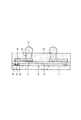
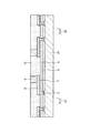
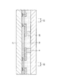
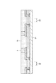
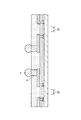
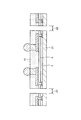
2 接続パッド
3 絶縁膜
5 保護膜
7 下地金属層
8 配線
9 柱状電極
10 封止膜
11 半田ボール
21 半導体ウエハ
22 ダイシングライン
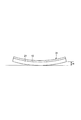
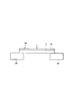
31 試料
32 試料チップ
Claims (5)
- 半導体ウエハ上に複数の柱状電極が形成され、前記柱状電極の周囲に封止膜が形成されたものを用意する工程と、
表面粗さが0.1nm以上3nm以下である研削砥石を用いて、前記半導体ウエハの下面側を研削する工程と、
前記半導体ウエハおよび前記封止膜をダイシングして、複数個の半導体装置を得る工程と、
を有することを特徴とする半導体装置の製造方法。 - 請求項1に記載の発明において、前記研削砥石の砥粒は1〜3μmであることを特徴とする半導体装置の製造方法。
- 請求項1に記載の発明において、前記研削砥石の表面粗さは2nm以下であることを特徴とする半導体装置の製造方法。
- 請求項3に記載の発明において、前記研削砥石の砥粒は1μm以下であることを特徴とする半導体装置の製造方法。
- 請求項1に記載の発明において、前記半導体ウエハの下面側を研削した後に、前記柱状電極上に半田ボールを形成する工程を有することを特徴とする半導体装置の製造方法。
Priority Applications (1)
| Application Number | Priority Date | Filing Date | Title |
|---|---|---|---|
| JP2006351184A JP2008166340A (ja) | 2006-12-27 | 2006-12-27 | 半導体装置の製造方法 |
Applications Claiming Priority (1)
| Application Number | Priority Date | Filing Date | Title |
|---|---|---|---|
| JP2006351184A JP2008166340A (ja) | 2006-12-27 | 2006-12-27 | 半導体装置の製造方法 |
Publications (1)
| Publication Number | Publication Date |
|---|---|
| JP2008166340A true JP2008166340A (ja) | 2008-07-17 |
Family
ID=39695472
Family Applications (1)
| Application Number | Title | Priority Date | Filing Date |
|---|---|---|---|
| JP2006351184A Pending JP2008166340A (ja) | 2006-12-27 | 2006-12-27 | 半導体装置の製造方法 |
Country Status (1)
| Country | Link |
|---|---|
| JP (1) | JP2008166340A (ja) |
Citations (5)
| Publication number | Priority date | Publication date | Assignee | Title |
|---|---|---|---|---|
| JP2001196404A (ja) * | 2000-01-11 | 2001-07-19 | Fujitsu Ltd | 半導体装置及びその製造方法 |
| JP2001223232A (ja) * | 2000-02-08 | 2001-08-17 | Matsushita Electric Ind Co Ltd | 半導体装置の製造方法 |
| JP2004296761A (ja) * | 2003-03-27 | 2004-10-21 | Mitsumi Electric Co Ltd | 半導体装置 |
| WO2006008824A1 (ja) * | 2004-07-16 | 2006-01-26 | Renesas Technology Corp. | 半導体集積回路装置の製造方法 |
| JP2007214502A (ja) * | 2006-02-13 | 2007-08-23 | Oki Electric Ind Co Ltd | 半導体装置およびその製造方法 |
-
2006
- 2006-12-27 JP JP2006351184A patent/JP2008166340A/ja active Pending
Patent Citations (5)
| Publication number | Priority date | Publication date | Assignee | Title |
|---|---|---|---|---|
| JP2001196404A (ja) * | 2000-01-11 | 2001-07-19 | Fujitsu Ltd | 半導体装置及びその製造方法 |
| JP2001223232A (ja) * | 2000-02-08 | 2001-08-17 | Matsushita Electric Ind Co Ltd | 半導体装置の製造方法 |
| JP2004296761A (ja) * | 2003-03-27 | 2004-10-21 | Mitsumi Electric Co Ltd | 半導体装置 |
| WO2006008824A1 (ja) * | 2004-07-16 | 2006-01-26 | Renesas Technology Corp. | 半導体集積回路装置の製造方法 |
| JP2007214502A (ja) * | 2006-02-13 | 2007-08-23 | Oki Electric Ind Co Ltd | 半導体装置およびその製造方法 |
Similar Documents
| Publication | Publication Date | Title |
|---|---|---|
| US9012269B2 (en) | Reducing warpage for fan-out wafer level packaging | |
| US7964446B2 (en) | Semiconductor device and method of manufacturing the same | |
| US11776838B2 (en) | Semiconductor package and manufacturing method thereof | |
| US8330279B2 (en) | Semiconductor device | |
| US20110156230A1 (en) | Multi-stacked semiconductor dice scale package structure and method of manufacturing same | |
| JP5610422B2 (ja) | 半導体装置及び半導体装置の製造方法 | |
| JP2008016508A (ja) | 半導体装置およびその製造方法 | |
| US20220367338A1 (en) | Package structure and manufacturing method thereof | |
| JP2007214563A (ja) | 半導体チップパッケージ | |
| JP2008166340A (ja) | 半導体装置の製造方法 | |
| TWI352411B (en) | Thinning method for fabricating dies arrangement p | |
| CN106611713A (zh) | 半导体封装体及其制作方法 | |
| TW466652B (en) | Wafer level package and its process thereof | |
| US20130256909A1 (en) | Patterned adhesive tape for backgrinding processes | |
| TW589726B (en) | Wafer level packaging process and structure thereof | |
| US6894389B2 (en) | Semiconductor device and manufacturing method therefor | |
| JP4337858B2 (ja) | 半導体装置 | |
| JP2005243909A (ja) | 表面保護テープおよび半導体装置の製造方法 | |
| JP2017069277A (ja) | 半導体装置及びその製造方法 | |
| JP4337859B2 (ja) | 半導体装置 | |
| JP2011060999A (ja) | 半導体装置及びその製造方法 | |
| JP2011014844A (ja) | 半導体装置の製造方法 | |
| JP5082333B2 (ja) | 半導体装置及び半導体装置の製造方法 | |
| JP2004047903A (ja) | 半導体装置およびその製造方法 | |
| JP4297153B2 (ja) | 半導体装置の製造方法 |
Legal Events
| Date | Code | Title | Description |
|---|---|---|---|
| RD04 | Notification of resignation of power of attorney |
Free format text: JAPANESE INTERMEDIATE CODE: A7424 Effective date: 20080515 |
|
| A621 | Written request for application examination |
Free format text: JAPANESE INTERMEDIATE CODE: A621 Effective date: 20091221 |
|
| A711 | Notification of change in applicant |
Free format text: JAPANESE INTERMEDIATE CODE: A712 Effective date: 20111115 |
|
| A131 | Notification of reasons for refusal |
Free format text: JAPANESE INTERMEDIATE CODE: A131 Effective date: 20120207 |
|
| A521 | Request for written amendment filed |
Free format text: JAPANESE INTERMEDIATE CODE: A523 Effective date: 20120323 |
|
| A02 | Decision of refusal |
Free format text: JAPANESE INTERMEDIATE CODE: A02 Effective date: 20120522 |