JP2008166340A - Manufacturing method of semiconductor device - Google Patents
Manufacturing method of semiconductor device Download PDFInfo
- Publication number
- JP2008166340A JP2008166340A JP2006351184A JP2006351184A JP2008166340A JP 2008166340 A JP2008166340 A JP 2008166340A JP 2006351184 A JP2006351184 A JP 2006351184A JP 2006351184 A JP2006351184 A JP 2006351184A JP 2008166340 A JP2008166340 A JP 2008166340A
- Authority
- JP
- Japan
- Prior art keywords
- semiconductor wafer
- grinding wheel
- semiconductor
- semiconductor device
- manufacturing
- Prior art date
- Legal status (The legal status is an assumption and is not a legal conclusion. Google has not performed a legal analysis and makes no representation as to the accuracy of the status listed.)
- Pending
Links
Images

Classifications
-
- H10W72/012—
Landscapes
- Mechanical Treatment Of Semiconductor (AREA)
- Dicing (AREA)
Abstract
【課題】 薄型化のため、上に封止膜が形成された半導体ウエハの下面側を研削しても、半導体ウエハの反りを低減し、且つ、半導体ウエハのダイシングにより個片化された半導体基板の抗折強度を比較的高くする。
【解決手段】 表面粗さが0.1nm以上3nm以下である研削砥石を用いて、半導体ウエハ21の下面側を研削すると、半導体ウエハ21上に封止膜10が形成されていても、半導体ウエハ21の反りを低減することができ、且つ、半導体ウエハ21のダイシングにより個片化された半導体基板の抗折強度を比較的高くすることができる。
【選択図】 図5PROBLEM TO BE SOLVED: To reduce the warpage of a semiconductor wafer even if the lower surface side of a semiconductor wafer having a sealing film formed thereon is ground for thinning, and to separate the semiconductor substrate by dicing the semiconductor wafer The bending strength of is relatively high.
When a lower surface side of a semiconductor wafer is ground by using a grinding wheel having a surface roughness of 0.1 nm or more and 3 nm or less, even if a sealing film 10 is formed on the semiconductor wafer 21, the semiconductor wafer 21 can be reduced, and the bending strength of the semiconductor substrate separated by dicing of the semiconductor wafer 21 can be made relatively high.
[Selection] Figure 5
Description
この発明は半導体装置の製造方法に関する。 The present invention relates to a method for manufacturing a semiconductor device.
従来の半導体装置の製造方法には、半導体ウエハ上に形成された複数の配線の接続パッド部上面に柱状電極を形成し、柱状電極および配線を含む半導体ウエハ上にエポキシ系樹脂等からなる封止膜を形成し、封止膜の上面側を研削して、柱状電極の上面を露出させるとともに、柱状電極の上面を含む封止膜の上面を平坦化し、柱状電極の上面に半田ボールを形成し、半導体ウエハおよび封止膜をダイシングして複数個の半導体装置を得る方法がある(例えば、特許文献1参照)。 In a conventional method of manufacturing a semiconductor device, a columnar electrode is formed on the upper surface of a connection pad portion of a plurality of wirings formed on a semiconductor wafer, and sealing made of an epoxy resin or the like on the semiconductor wafer including the columnar electrodes and the wirings Form a film, grind the upper surface side of the sealing film to expose the upper surface of the columnar electrode, flatten the upper surface of the sealing film including the upper surface of the columnar electrode, and form solder balls on the upper surface of the columnar electrode There is a method of obtaining a plurality of semiconductor devices by dicing a semiconductor wafer and a sealing film (see, for example, Patent Document 1).
ところで、この種の従来の半導体装置には、薄型化のため、半導体ウエハのダイシングにより個片化された半導体基板の厚さを薄くしたものがある。従来のこのような半導体装置の製造方法では、半導体ウエハの厚さを当初から薄くすると、破損しやすいため、半導体ウエハ上に形成されたエポキシ系樹脂等からなる封止膜で補強し、封止膜の上面側を研削した後に、半導体ウエハの下面側を研削している。 By the way, in this type of conventional semiconductor device, there is one in which the thickness of a semiconductor substrate separated by dicing of a semiconductor wafer is reduced in order to reduce the thickness. In such a conventional method for manufacturing a semiconductor device, if the thickness of the semiconductor wafer is reduced from the beginning, it is easily damaged. Therefore, the semiconductor wafer is reinforced and sealed with a sealing film made of an epoxy resin or the like formed on the semiconductor wafer. After the upper surface side of the film is ground, the lower surface side of the semiconductor wafer is ground.
しかしながら、上記従来の半導体装置の製造方法では、半導体ウエハと封止膜との熱膨張係数差に起因する応力により、半導体ウエハに反りが生じ、特に、大径例えば直径200mm(8インチ)以上の半導体ウエハの下面側を研削した後においては半導体ウエハの反りが大きくなり、それ以後の工程への搬送やそれ以後の工程での加工精度に支障を来すという問題があった。また、半導体ウエハの厚さを薄くすると、半導体ウエハのダイシングにより個片化された半導体基板の抗折強度が低下するという問題があった。 However, in the conventional method for manufacturing a semiconductor device, the semiconductor wafer is warped due to the stress caused by the difference in thermal expansion coefficient between the semiconductor wafer and the sealing film, and in particular, has a large diameter of, for example, 200 mm (8 inches) or more in diameter. After the lower surface side of the semiconductor wafer is ground, the warpage of the semiconductor wafer becomes large, and there is a problem that the transfer to the subsequent process and the processing accuracy in the subsequent process are hindered. Further, when the thickness of the semiconductor wafer is reduced, there is a problem that the bending strength of the semiconductor substrate separated by dicing of the semiconductor wafer is lowered.
そこで、この発明は、薄型化のため、上に封止膜が形成された半導体ウエハの下面側を研削しても、半導体ウエハの反りを低減することができ、且つ、半導体基板の抗折強度を比較的高くすることができる半導体装置の製造方法を提供することを目的とする。 Therefore, the present invention can reduce the warpage of the semiconductor wafer and reduce the bending strength of the semiconductor substrate even if the lower surface side of the semiconductor wafer having the sealing film formed thereon is ground for thinning. It is an object of the present invention to provide a method for manufacturing a semiconductor device that can increase the relative resistance.
請求項1に記載の発明は、半導体ウエハ上に複数の柱状電極が形成され、前記柱状電極の周囲に封止膜が形成されたものを用意する工程と、表面粗さが0.1nm以上3nm以下である研削砥石を用いて、前記半導体ウエハの下面側を研削する工程と、前記半導体ウエハおよび前記封止膜をダイシングして、複数個の半導体装置を得る工程と、を有することを特徴とするものである。
請求項2に記載の発明は、請求項1に記載の発明において、前記研削砥石の砥粒は1〜3μmであることを特徴とするものである。
請求項3に記載の発明は、請求項1に記載の発明において、前記研削砥石の表面粗さは2nm以下であることを特徴とするものである。
請求項4に記載の発明は、請求項3に記載の発明において、前記研削砥石の砥粒は1μm以下であることを特徴とするものである。
請求項5に記載の発明は、請求項1に記載の発明において、前記半導体ウエハの下面側を研削した後に、前記柱状電極上に半田ボールを形成する工程を有することを特徴とするものである。
According to the first aspect of the present invention, there is provided a step of preparing a plurality of columnar electrodes formed on a semiconductor wafer and a sealing film formed around the columnar electrodes, and a surface roughness of 0.1 nm to 3 nm. Using a grinding wheel which is the following, grinding the lower surface side of the semiconductor wafer, and dicing the semiconductor wafer and the sealing film to obtain a plurality of semiconductor devices, To do.
The invention according to
The invention according to
The invention described in
The invention according to
この発明によれば、表面粗さが0.1nm以上3nm以下である研削砥石を用いて、半導体ウエハの下面側を研削することにより、半導体ウエハ上に封止膜が形成されていても、半導体ウエハの反りを低減することができ、且つ、半導体基板の抗折強度を比較的高くすることができる。 According to this invention, even if the sealing film is formed on the semiconductor wafer by grinding the lower surface side of the semiconductor wafer using a grinding wheel having a surface roughness of 0.1 nm or more and 3 nm or less, the semiconductor The warpage of the wafer can be reduced, and the bending strength of the semiconductor substrate can be made relatively high.
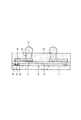
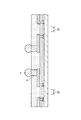
図1はこの発明の製造方法により製造された半導体装置の一例の断面図を示す。この半導体装置は、一般的にはCSP(chip size package)と呼ばれるものであり、シリコン基板(半導体基板)1を備えている。シリコン基板1の上面には所定の機能の集積回路(図示せず)が設けられ、上面周辺部にはアルミニウム系金属等からなる複数の接続パッド2が集積回路に接続されて設けられている。
FIG. 1 is a sectional view showing an example of a semiconductor device manufactured by the manufacturing method of the present invention. This semiconductor device is generally called a CSP (chip size package) and includes a silicon substrate (semiconductor substrate) 1. An integrated circuit (not shown) having a predetermined function is provided on the upper surface of the
接続パッド2の中央部を除くシリコン基板1の上面には酸化シリコン等からなる絶縁膜3が設けられ、接続パッド2の中央部は絶縁膜3に設けられた開口部4を介して露出されている。絶縁膜3の上面にはポリイミド系樹脂等からなる保護膜5が設けられている。絶縁膜3の開口部4に対応する部分における保護膜5には開口部6が設けられている。
An
保護膜5の上面には銅等からなる下地金属層7が設けられている。下地金属層7の上面全体には銅からなる配線8が設けられている。下地金属層7を含む配線8の一端部は、絶縁膜3および保護膜5の開口部4、6を介して接続パッド2に接続されている。
A
配線8の接続パッド部上面には銅からなる柱状電極9が設けられている。配線8を含む保護膜5の上面にはエポキシ系樹脂等からなる封止膜10がその上面が柱状電極9の上面と面一となるように設けられている。柱状電極9の上面には半田ボール11が設けられている。
A
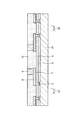
次に、この半導体装置の製造方法の一例について説明する。まず、図2に示すように、ウエハ状態のシリコン基板(以下、半導体ウエハ21という)上に、接続パッド2、絶縁膜3、保護膜5、下地金属層7、配線8、柱状電極9および封止膜10が形成され、半田ボール11が形成されていないものを用意する。
Next, an example of a method for manufacturing this semiconductor device will be described. First, as shown in FIG. 2, on a silicon substrate (hereinafter referred to as a semiconductor wafer 21) in a wafer state, the
この場合、半導体ウエハ21の厚さは、図1に示すシリコン基板1の厚さよりもある程度厚くなっている。また、封止膜10は柱状電極9の周囲に形成され、柱状電極9の上面は露出されている。なお、図2において、符号22で示す領域はダイシングラインに対応する領域である。
In this case, the thickness of the
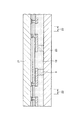
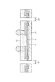
次に、図2に示すものの上下を反転し、図3に示すように、柱状電極9の下面を含む封止膜10の下面を保護テープ23の上面に貼り付ける。次に、図4に示すように、半導体ウエハ21の上面側を研削砥石(図示せず)を用いて適宜に研削し、半導体ウエハ21の厚さを適宜に薄くする。この研削の詳細については後で説明する。
2 is turned upside down, and the lower surface of the
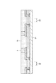
次に、図4に示すものの上下を反転し、次いで、保護テープ23を剥離すると、図5に示すようになる。この状態では、図2に示す当初用意したものと比較すると、半導体ウエハ21の下面側が適宜に研削され、半導体ウエハ21の厚さが適宜に薄くなっている。
Next, when the one shown in FIG. 4 is turned upside down and then the
次に、図6に示すように、柱状電極9の上面に半田ボール11を形成する。次に、図7に示すように、ダイシングライン22に沿って、封止膜10、保護膜5、絶縁膜3および半導体ウエハ21をダイシングすると、図1に示す半導体装置が複数個得られる。
Next, as shown in FIG. 6,
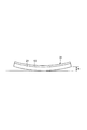
次に、図4に示すような研削工程の具体例について説明する。まず、図8を参照して説明すると、半導体ウエハ21として直径200mm(8インチ)、厚さ700μmのものを用い、この半導体ウエハ21の上面にエポキシ系樹脂からなる厚さ90μmの封止膜10のみを形成した試料31を用意した。
Next, a specific example of the grinding process as shown in FIG. 4 will be described. First, referring to FIG. 8, a
そして、研削砥石としてJIS規格の砥石番手#2000(表面粗さ6.6nm、砥粒4〜6μm)、#5000(表面粗さ3nm以下、砥粒1〜3μm)および#8000(表面粗さ2nm以下、砥粒1μm以下)のものを用い、試料31の半導体ウエハ21の下面側をその厚さが460μm(試料31の厚さ550μm)となるまで研削した。すると、図8に示すように、半導体ウエハ21の中央部に対して外周部が浮き上がるような反りが発生した。
As grinding wheels, JIS standard grinding wheel count # 2000 (surface roughness 6.6 nm,
そして、半導体ウエハ21の下面の中央部に対する外周端部の高さH(以下、反り量Hという)を測定したところ、#2000の研削砥石を用いた場合には0.72mmであり、#5000の研削砥石を用いた場合には0.39mmであり、#8000の研削砥石を用いた場合には0.36mmであった。 Then, when the height H of the outer peripheral end with respect to the central portion of the lower surface of the semiconductor wafer 21 (hereinafter referred to as warpage amount H) was measured, it was 0.72 mm when using a # 2000 grinding wheel, and # 5000. Was 0.39 mm when the # 1 grinding wheel was used, and 0.36 mm when the # 8000 grinding wheel was used.
すなわち、#5000の研削砥石を用いた場合の反り量Hは#2000の研削砥石を用いた場合の反り量Hの1/2強であり、#8000の研削砥石を用いた場合の反り量Hは#2000の研削砥石を用いた場合の反り量Hの1/2であった。したがって、半導体ウエハ21の下面側を研削するための研削砥石しては、#2000のものは好ましくなく、#5000のものが好ましく、#8000のものがより好ましい。
That is, the warpage amount H when the # 5000 grinding wheel is used is slightly more than half of the warpage amount H when the # 2000 grinding wheel is used, and the warpage amount H when the # 8000 grinding wheel is used. Was 1/2 of the amount of warpage H when using a # 2000 grinding wheel. Accordingly, the grinding wheel for grinding the lower surface side of the
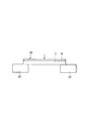
次に、抗折強度試験について説明する。この場合、研削砥石として#2000、#5000および#8000のものを用い、試料31の半導体ウエハ21の下面側をその厚さが460μm(試料31の厚さ550μm)、310μm(試料31の厚さ400μm)、210μm(試料31の厚さ300μm)および160μm(試料31の厚さ250μm)となるまで研削し、ダイシングにより仕上り寸法5.96mm×5.96mmの試料チップ32(図9参照)を得た。
Next, the bending strength test will be described. In this case, grinding wheels of # 2000, # 5000 and # 8000 are used, and the thickness of the lower surface side of the
そして、図9に示すように、試料チップ32のシリコン基板1を一対の支持部材33、34の上面に載置し、矢印で示すように、試料チップ32の封止膜10の上面中央部に荷重1.0mm/sec(260gf・cm/sec)を加え、シリコン基板1の抗折強度を測定した。ここで、チップマウンターを用いて図1に示すような半導体装置を実装する際に、シリコン基板1に掛かる荷重が800gfであると、抗折強度が1kgf以上であれば、シリコン基板1が破損することはない。
Then, as shown in FIG. 9, the
さて、#2000の研削砥石を用いた場合には、試料チップ32の厚さが550μmおよび400μmであると、シリコン基板1の抗折強度が0.79kgfおよび0.85kgfであり、いずれの場合も1kgf未満であり、好ましくない。
When the # 2000 grinding wheel is used, if the thickness of the
#5000の研削砥石を用いた場合には、試料チップ32の厚さが550μmおよび400μmであると、シリコン基板1の抗折強度が3.57kgfおよび2.045kgfであり、いずれの場合も1kgf以上であり、好ましい。しかし、試料チップ32の厚さが300μmおよび250μmであると、シリコン基板1の抗折強度が0.93kgfおよび0.36kgfであり、いずれの場合も1kgf未満であり、好ましくない。
When a # 5000 grinding wheel is used, if the thickness of the
#8000の研削砥石を用いた場合には、試料チップ32の厚さが550μm、400μmおよび300μmであると、シリコン基板1の抗折強度が4.42kgf、1.43kgfおよび1.15kgfであり、いずれの場合も1kgf以上であり、好ましい。しかし、試料チップ32の厚さが250μmであると、シリコン基板1の抗折強度が1kgf未満の0.67kgfであり、好ましくない。
When the # 8000 grinding wheel is used, the bending strength of the
以上のことから、#2000の研削砥石を用いることは好ましくなく、#5000の研削砥石を用いた場合には、試料チップ32の厚さが400μm以上であれば、シリコン基板1の抗折強度を比較的高くすることができ、#8000の研削砥石を用いた場合には、試料チップ32の厚さが300μm以上であれば、シリコン基板1の抗折強度を比較的高くすることができる。
From the above, it is not preferable to use a grinding wheel of # 2000. When a grinding wheel of # 5000 is used, the bending strength of the
なお、研削砥石としては砥石番手が#8000よりも大きいものを用いてもよく、例えば#30000(表面粗さ0.1〜0.3nm、砥粒0.1μm)のものを用いてもよい。また、この発明は、CSPと呼ばれる半導体装置に限らず、例えば、絶縁膜3の開口部4を介して露出された接続パッド2上に下地金属層および柱状電極を形成し、柱状電極の周囲における絶縁膜3上に封止膜を形成し、柱状電極上に半田ボールを形成した半導体装置にも適用することができる。
In addition, as a grinding wheel, a thing with a grindstone number larger than # 8000 may be used, for example, the thing of # 30000 (surface roughness 0.1-0.3 nm, abrasive grain 0.1 micrometer) may be used. In addition, the present invention is not limited to a semiconductor device called a CSP. For example, a base metal layer and a columnar electrode are formed on the
1 シリコン基板
2 接続パッド
3 絶縁膜
5 保護膜
7 下地金属層
8 配線
9 柱状電極
10 封止膜
11 半田ボール
21 半導体ウエハ
22 ダイシングライン
31 試料
32 試料チップ
DESCRIPTION OF
Claims (5)
表面粗さが0.1nm以上3nm以下である研削砥石を用いて、前記半導体ウエハの下面側を研削する工程と、
前記半導体ウエハおよび前記封止膜をダイシングして、複数個の半導体装置を得る工程と、
を有することを特徴とする半導体装置の製造方法。 Preparing a plurality of columnar electrodes formed on a semiconductor wafer and having a sealing film formed around the columnar electrodes;
Grinding the lower surface side of the semiconductor wafer using a grinding wheel having a surface roughness of 0.1 nm or more and 3 nm or less;
Dicing the semiconductor wafer and the sealing film to obtain a plurality of semiconductor devices;
A method for manufacturing a semiconductor device, comprising:
Priority Applications (1)
| Application Number | Priority Date | Filing Date | Title |
|---|---|---|---|
| JP2006351184A JP2008166340A (en) | 2006-12-27 | 2006-12-27 | Manufacturing method of semiconductor device |
Applications Claiming Priority (1)
| Application Number | Priority Date | Filing Date | Title |
|---|---|---|---|
| JP2006351184A JP2008166340A (en) | 2006-12-27 | 2006-12-27 | Manufacturing method of semiconductor device |
Publications (1)
| Publication Number | Publication Date |
|---|---|
| JP2008166340A true JP2008166340A (en) | 2008-07-17 |
Family
ID=39695472
Family Applications (1)
| Application Number | Title | Priority Date | Filing Date |
|---|---|---|---|
| JP2006351184A Pending JP2008166340A (en) | 2006-12-27 | 2006-12-27 | Manufacturing method of semiconductor device |
Country Status (1)
| Country | Link |
|---|---|
| JP (1) | JP2008166340A (en) |
Citations (5)
| Publication number | Priority date | Publication date | Assignee | Title |
|---|---|---|---|---|
| JP2001196404A (en) * | 2000-01-11 | 2001-07-19 | Fujitsu Ltd | Semiconductor device and manufacturing method thereof |
| JP2001223232A (en) * | 2000-02-08 | 2001-08-17 | Matsushita Electric Ind Co Ltd | Method for manufacturing semiconductor device |
| JP2004296761A (en) * | 2003-03-27 | 2004-10-21 | Mitsumi Electric Co Ltd | Semiconductor device |
| WO2006008824A1 (en) * | 2004-07-16 | 2006-01-26 | Renesas Technology Corp. | Method for manufacturing semiconductor integrated circuit device |
| JP2007214502A (en) * | 2006-02-13 | 2007-08-23 | Oki Electric Ind Co Ltd | Semiconductor device and manufacturing method thereof |
-
2006
- 2006-12-27 JP JP2006351184A patent/JP2008166340A/en active Pending
Patent Citations (5)
| Publication number | Priority date | Publication date | Assignee | Title |
|---|---|---|---|---|
| JP2001196404A (en) * | 2000-01-11 | 2001-07-19 | Fujitsu Ltd | Semiconductor device and manufacturing method thereof |
| JP2001223232A (en) * | 2000-02-08 | 2001-08-17 | Matsushita Electric Ind Co Ltd | Method for manufacturing semiconductor device |
| JP2004296761A (en) * | 2003-03-27 | 2004-10-21 | Mitsumi Electric Co Ltd | Semiconductor device |
| WO2006008824A1 (en) * | 2004-07-16 | 2006-01-26 | Renesas Technology Corp. | Method for manufacturing semiconductor integrated circuit device |
| JP2007214502A (en) * | 2006-02-13 | 2007-08-23 | Oki Electric Ind Co Ltd | Semiconductor device and manufacturing method thereof |
Similar Documents
| Publication | Publication Date | Title |
|---|---|---|
| US9012269B2 (en) | Reducing warpage for fan-out wafer level packaging | |
| US7964446B2 (en) | Semiconductor device and method of manufacturing the same | |
| US11776838B2 (en) | Semiconductor package and manufacturing method thereof | |
| US8330279B2 (en) | Semiconductor device | |
| US20110156230A1 (en) | Multi-stacked semiconductor dice scale package structure and method of manufacturing same | |
| JP5610422B2 (en) | Semiconductor device and manufacturing method of semiconductor device | |
| JP2008016508A (en) | Semiconductor device and manufacturing method thereof | |
| US20220367338A1 (en) | Package structure and manufacturing method thereof | |
| JP2007214563A (en) | Semiconductor chip package | |
| JP2008166340A (en) | Manufacturing method of semiconductor device | |
| TWI352411B (en) | Thinning method for fabricating dies arrangement p | |
| CN106611713A (en) | Semiconductor package and method for forming the same | |
| TW466652B (en) | Wafer level package and its process thereof | |
| US20130256909A1 (en) | Patterned adhesive tape for backgrinding processes | |
| TW589726B (en) | Wafer level packaging process and structure thereof | |
| US6894389B2 (en) | Semiconductor device and manufacturing method therefor | |
| JP4337858B2 (en) | Semiconductor device | |
| JP2005243909A (en) | Surface protective tape and method for manufacturing semiconductor device | |
| JP2017069277A (en) | Semiconductor device and manufacturing method of the same | |
| JP4337859B2 (en) | Semiconductor device | |
| JP2011060999A (en) | Semiconductor device and method for manufacturing the same | |
| JP2011014844A (en) | Method of manufacturing semiconductor device | |
| JP5082333B2 (en) | Semiconductor device and manufacturing method of semiconductor device | |
| JP2004047903A (en) | Semiconductor device and method of manufacturing the same | |
| JP4297153B2 (en) | Manufacturing method of semiconductor device |
Legal Events
| Date | Code | Title | Description |
|---|---|---|---|
| RD04 | Notification of resignation of power of attorney |
Free format text: JAPANESE INTERMEDIATE CODE: A7424 Effective date: 20080515 |
|
| A621 | Written request for application examination |
Free format text: JAPANESE INTERMEDIATE CODE: A621 Effective date: 20091221 |
|
| A711 | Notification of change in applicant |
Free format text: JAPANESE INTERMEDIATE CODE: A712 Effective date: 20111115 |
|
| A131 | Notification of reasons for refusal |
Free format text: JAPANESE INTERMEDIATE CODE: A131 Effective date: 20120207 |
|
| A521 | Request for written amendment filed |
Free format text: JAPANESE INTERMEDIATE CODE: A523 Effective date: 20120323 |
|
| A02 | Decision of refusal |
Free format text: JAPANESE INTERMEDIATE CODE: A02 Effective date: 20120522 |