JP2007505995A - 無電解堆積のエンドポイントを検出するための装置および方法 - Google Patents
無電解堆積のエンドポイントを検出するための装置および方法 Download PDFInfo
- Publication number
- JP2007505995A JP2007505995A JP2006527044A JP2006527044A JP2007505995A JP 2007505995 A JP2007505995 A JP 2007505995A JP 2006527044 A JP2006527044 A JP 2006527044A JP 2006527044 A JP2006527044 A JP 2006527044A JP 2007505995 A JP2007505995 A JP 2007505995A
- Authority
- JP
- Japan
- Prior art keywords
- substrate
- electromagnetic radiation
- detector
- electroless deposition
- intensity
- Prior art date
- Legal status (The legal status is an assumption and is not a legal conclusion. Google has not performed a legal analysis and makes no representation as to the accuracy of the status listed.)
- Granted
Links
Images


Classifications
-
- C—CHEMISTRY; METALLURGY
- C23—COATING METALLIC MATERIAL; COATING MATERIAL WITH METALLIC MATERIAL; CHEMICAL SURFACE TREATMENT; DIFFUSION TREATMENT OF METALLIC MATERIAL; COATING BY VACUUM EVAPORATION, BY SPUTTERING, BY ION IMPLANTATION OR BY CHEMICAL VAPOUR DEPOSITION, IN GENERAL; INHIBITING CORROSION OF METALLIC MATERIAL OR INCRUSTATION IN GENERAL
- C23C—COATING METALLIC MATERIAL; COATING MATERIAL WITH METALLIC MATERIAL; SURFACE TREATMENT OF METALLIC MATERIAL BY DIFFUSION INTO THE SURFACE, BY CHEMICAL CONVERSION OR SUBSTITUTION; COATING BY VACUUM EVAPORATION, BY SPUTTERING, BY ION IMPLANTATION OR BY CHEMICAL VAPOUR DEPOSITION, IN GENERAL
- C23C18/00—Chemical coating by decomposition of either liquid compounds or solutions of the coating forming compounds, without leaving reaction products of surface material in the coating; Contact plating
- C23C18/16—Chemical coating by decomposition of either liquid compounds or solutions of the coating forming compounds, without leaving reaction products of surface material in the coating; Contact plating by reduction or substitution, e.g. electroless plating
- C23C18/1601—Process or apparatus
- C23C18/1633—Process of electroless plating
- C23C18/1655—Process features
- C23C18/1664—Process features with additional means during the plating process
- C23C18/1667—Radiant energy, e.g. laser
-
- C—CHEMISTRY; METALLURGY
- C23—COATING METALLIC MATERIAL; COATING MATERIAL WITH METALLIC MATERIAL; CHEMICAL SURFACE TREATMENT; DIFFUSION TREATMENT OF METALLIC MATERIAL; COATING BY VACUUM EVAPORATION, BY SPUTTERING, BY ION IMPLANTATION OR BY CHEMICAL VAPOUR DEPOSITION, IN GENERAL; INHIBITING CORROSION OF METALLIC MATERIAL OR INCRUSTATION IN GENERAL
- C23C—COATING METALLIC MATERIAL; COATING MATERIAL WITH METALLIC MATERIAL; SURFACE TREATMENT OF METALLIC MATERIAL BY DIFFUSION INTO THE SURFACE, BY CHEMICAL CONVERSION OR SUBSTITUTION; COATING BY VACUUM EVAPORATION, BY SPUTTERING, BY ION IMPLANTATION OR BY CHEMICAL VAPOUR DEPOSITION, IN GENERAL
- C23C18/00—Chemical coating by decomposition of either liquid compounds or solutions of the coating forming compounds, without leaving reaction products of surface material in the coating; Contact plating
- C23C18/16—Chemical coating by decomposition of either liquid compounds or solutions of the coating forming compounds, without leaving reaction products of surface material in the coating; Contact plating by reduction or substitution, e.g. electroless plating
- C23C18/1601—Process or apparatus
- C23C18/1633—Process of electroless plating
- C23C18/1646—Characteristics of the product obtained
- C23C18/165—Multilayered product
- C23C18/1651—Two or more layers only obtained by electroless plating
-
- C—CHEMISTRY; METALLURGY
- C23—COATING METALLIC MATERIAL; COATING MATERIAL WITH METALLIC MATERIAL; CHEMICAL SURFACE TREATMENT; DIFFUSION TREATMENT OF METALLIC MATERIAL; COATING BY VACUUM EVAPORATION, BY SPUTTERING, BY ION IMPLANTATION OR BY CHEMICAL VAPOUR DEPOSITION, IN GENERAL; INHIBITING CORROSION OF METALLIC MATERIAL OR INCRUSTATION IN GENERAL
- C23C—COATING METALLIC MATERIAL; COATING MATERIAL WITH METALLIC MATERIAL; SURFACE TREATMENT OF METALLIC MATERIAL BY DIFFUSION INTO THE SURFACE, BY CHEMICAL CONVERSION OR SUBSTITUTION; COATING BY VACUUM EVAPORATION, BY SPUTTERING, BY ION IMPLANTATION OR BY CHEMICAL VAPOUR DEPOSITION, IN GENERAL
- C23C18/00—Chemical coating by decomposition of either liquid compounds or solutions of the coating forming compounds, without leaving reaction products of surface material in the coating; Contact plating
- C23C18/16—Chemical coating by decomposition of either liquid compounds or solutions of the coating forming compounds, without leaving reaction products of surface material in the coating; Contact plating by reduction or substitution, e.g. electroless plating
- C23C18/1601—Process or apparatus
- C23C18/1633—Process of electroless plating
- C23C18/1675—Process conditions
-
- G—PHYSICS
- G01—MEASURING; TESTING
- G01B—MEASURING LENGTH, THICKNESS OR SIMILAR LINEAR DIMENSIONS; MEASURING ANGLES; MEASURING AREAS; MEASURING IRREGULARITIES OF SURFACES OR CONTOURS
- G01B11/00—Measuring arrangements characterised by the use of optical techniques
- G01B11/02—Measuring arrangements characterised by the use of optical techniques for measuring length, width or thickness
- G01B11/06—Measuring arrangements characterised by the use of optical techniques for measuring length, width or thickness for measuring thickness ; e.g. of sheet material
- G01B11/0616—Measuring arrangements characterised by the use of optical techniques for measuring length, width or thickness for measuring thickness ; e.g. of sheet material of coating
- G01B11/0683—Measuring arrangements characterised by the use of optical techniques for measuring length, width or thickness for measuring thickness ; e.g. of sheet material of coating measurement during deposition or removal of the layer
-
- G—PHYSICS
- G01—MEASURING; TESTING
- G01N—INVESTIGATING OR ANALYSING MATERIALS BY DETERMINING THEIR CHEMICAL OR PHYSICAL PROPERTIES
- G01N21/00—Investigating or analysing materials by the use of optical means, i.e. using sub-millimetre waves, infrared, visible or ultraviolet light
- G01N21/84—Systems specially adapted for particular applications
- G01N21/8422—Investigating thin films, e.g. matrix isolation method
-
- G—PHYSICS
- G01—MEASURING; TESTING
- G01N—INVESTIGATING OR ANALYSING MATERIALS BY DETERMINING THEIR CHEMICAL OR PHYSICAL PROPERTIES
- G01N21/00—Investigating or analysing materials by the use of optical means, i.e. using sub-millimetre waves, infrared, visible or ultraviolet light
- G01N21/84—Systems specially adapted for particular applications
- G01N21/88—Investigating the presence of flaws or contamination
- G01N21/95—Investigating the presence of flaws or contamination characterised by the material or shape of the object to be examined
- G01N21/9501—Semiconductor wafers
Landscapes
- Chemical & Material Sciences (AREA)
- Physics & Mathematics (AREA)
- Materials Engineering (AREA)
- General Chemical & Material Sciences (AREA)
- Organic Chemistry (AREA)
- Metallurgy (AREA)
- Mechanical Engineering (AREA)
- General Physics & Mathematics (AREA)
- Engineering & Computer Science (AREA)
- Chemical Kinetics & Catalysis (AREA)
- Biochemistry (AREA)
- Pathology (AREA)
- Immunology (AREA)
- General Health & Medical Sciences (AREA)
- Health & Medical Sciences (AREA)
- Analytical Chemistry (AREA)
- Life Sciences & Earth Sciences (AREA)
- Optics & Photonics (AREA)
- Mathematical Physics (AREA)
- Chemically Coating (AREA)
- Electrodes Of Semiconductors (AREA)
- Internal Circuitry In Semiconductor Integrated Circuit Devices (AREA)
Abstract
【選択図】 図2A
Description
[0001]本発明は、一般的に、基板上に形成されたサブミクロンアパーチャの上に導電性材料を堆積するための装置および方法に関する。
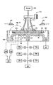
[0081]図5は、本明細書に説明されたような触媒層および/または導電性材料層の堆積に有用なチャンバ160の一実施形態の概略断面図を示す。当然、チャンバ160はまた、触媒層および導電性材料層以外の他のタイプの層を堆積するように構成されてもよい。2002年1月1日に提出された、「Electroless Deposition Apparatus」と題された米国特許出願第10/059,572号[AMAT 5840.03]に説明されている、触媒層および金属層を無電解堆積するための装置が、本明細書で請求された態様および開示と矛盾しない限り本明細書に参照して組み込まれる。チャンバ160は、上部152と、側壁154と底部156とを備える処理コンパートメント150を含む。基板サポート162がチャンバ160の略中央の場所に配置され、フェースアップ位置で基板10を受け取るように適合された基板受け取り表面164を含む。チャンバ160はさらに、基板受け取り基板164に対して基板10を保持するように構成されたクランプリング166を含む。一態様において、クランプリング166は、基板10と加熱された基板サポート162間の熱転送を改良する。通常、基板サポート162は、外部電源と、基板サポート162に埋め込まれた1つ以上の抵抗要素とを使用して加熱されてもよい。別の態様において、クランプリング166は基板サポート162の回転中に基板を保持する。さらに別の態様において、クランプリング166の厚さは、処理中に基板10の表面に堆積流体168のプールを形成するために使用される。
[0099]図7は、触媒層および/または導電性材料層の堆積に有用なチャンバ170の別の実施形態の概略断面図を示す。チャンバ170は、フェースダウン位置で基板10を保持するように適合された基板受け取り表面174を有する基板ホルダ172を含む。基板ホルダ172は基板10を所望の温度に加熱するために加熱されてもよい。基板ホルダ172の基板受け取り表面174は、基板10の均一な加熱を提供するために基板10のバックサイドを実質的に受け取るようにサイズ設定されてもよい。基板ホルダ172はさらに、基板10のバックサイドに真空を供給して基板10を基板ホルダ172に真空チャックする、真空源183に結合された真空ポート173を含む。基板ホルダ172はさらに、基板10のバックサイドに対する、かつ真空ポート173への流体の流れを防ぐ真空シール181および液体シール182を含んでもよい。チャンバ170はさらに、流体ポート177などの流体入力を有するボウル176を備える。流体ポート177は流体源178a〜c、流体リターン179a〜cおよび/またはガス源180に結合されてもよい。一実施形態において、流体廃棄ドレイン184は処理中に使用された流体を収集するように適合可能である。
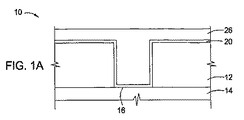
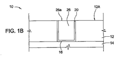
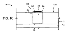
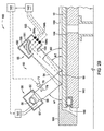
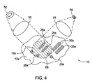
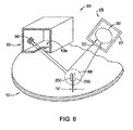
[00104]図8は、複数の検出部材250が基板の表面に追加されて、無電解堆積プロセスを検出および監視する検出システム60の能力を高める本発明の一態様を図示する。本実施形態において、検出部材250は一般的に、部材表面26aと同じ金属製材料から作られる基板の表面上に1つ以上のエリアを含む。検出部材250は、デバイス、あるいは普通半導体基板の表面に見られる「スクライブライン」のパッシブ部材である「リソグラフィックマーク」に追加されてもよい。検出部材250は任意の形状(例えば、円形、楕円形、矩形など)であってもよく、一般的に、長さ約100ナノメートル〜約100マイクロメートルの主要な寸法を有する基板の表面上のエリアをカバーすることが想定される。別の実施形態において、検出部材250は、発射された放射の所望の波長に比例して間隔をあけられる(「X」と示される)同じサイズの個々のより小さな検出部材250のアレイによって定義される。検出部材250のアレイのサイズおよび間隔は、反射された放射が1つ以上の波長で建設的または破壊的干渉を呈するように選択される。本実施形態において、(複数の)無電解堆積膜の成長は基板の表面上の検出部材250のアレイの物理的サイズおよび間隔を変化させることによって、建設的または破壊的干渉を呈する波長を変える。建設的かつ破壊的干渉を呈する反射された波長の変化と、種々の波長での強度の変化によって、検出システムは堆積膜の成長を検出できるようになる。信号対雑音比に対する迷光の効果を削減するために、検出システム60および基板の表面上のビューイングエリア68は環境光源からカバーまたは遮断される必要があると思われる。スリット、狭いアパーチャ(開口53a)はまた、検出器によって収集された放射量をコントロールして検出プロセスを高めかつ信号対雑音比を改良するために、検出システム55に追加されてもよい。
Claims (19)
- 無電解堆積プロセスを監視するための装置であって、
チャンバと、
基板受け取り表面を有する、前記チャンバに配置された基板サポートと、
前記基板受け取り表面に向けられた電磁放射源と、
無電解堆積プロセス中に前記基板受け取り表面に搭載された基板の表面から反射された電磁放射の強度を検出する検出器と、
前記検出器からの信号を受け取り、かつ前記無電解堆積プロセスをコントロールするように適合されたコントローラと、
を備える装置。 - 前記電磁放射源が、約200ナノメートル〜約800ナノメートルの波長で電磁放射を放出する、請求項1に記載の装置。
- 前記電磁放射源が1つ以上の発光ダイオードを備える、請求項1に記載の装置。
- 前記検出器が2つ以上の検出器を備える、請求項1に記載の装置。
- 前記基板サポートを前記検出器に対して移動させるドライブ機構をさらに備える、請求項1に記載の装置。
- 前記検出器を前記基板サポートに対して移動させる第2のドライブ機構をさらに備える、請求項1に記載の装置。
- 前記検出器がスペクトロメーターである、請求項1に記載の装置。
- 前記電磁放射源から収集された前記電磁放射を受け取る光ファイバケーブルと、
前記反射された電磁放射または前記光ファイバケーブルからの前記電磁放射が検出器へと通過するようにする機械的スリットと、
前記機械的スリットを位置決めする機械的アクチュエータを使用して、前記反射された電磁放射または前記電磁放射の前記光ファイバケーブルから前記検出器への送信を選択的にコントロールするコントローラと、
をさらに備える、請求項1に記載の装置。 - 前記電磁放射源からの前記電磁放射の強度を検出する第2の検出器と、
前記検出器からの信号および前記第2の検出器からの信号を受け取り、かつ前記無電解堆積プロセスをコントロールするように適合されたコントローラと、
をさらに備える、請求項1に記載の装置。 - 前記コントローラに結合されたメモリをさらに備えており、前記メモリが、前記無電解堆積システムの動作を方向付けるコンピュータ読み取り可能なプログラムを内部に具現化しているコンピュータ読み取り可能な媒体を備えており、前記コンピュータ読み取り可能なプログラムが、
前記無電解堆積システムをコントロールして、
(i)処理をスタートさせる、
(ii)前記無電解堆積プロセス中に反射された電磁放射の強度を収集して、前記メモリに記憶する、
(iii)前記記憶されたデータを前記収集されたデータと比較する、そして
(iv)前記収集されたデータが閾値を超える場合に前記無電解堆積プロセスを停止させるコンピュータ命令を備える、請求項1に記載の装置。 - 表面に検出部材を有する基板であって、前記基板サポートの前記基板受け取り表面上に配置される基板と、
前記基板の前記表面に向けられた電磁放射源と、
無電解堆積プロセス中に前記検出部材から反射された電磁放射の強度を検出する検出器と、
前記検出器からの信号を受け取り、かつ前記無電解堆積プロセスをコントロールするように適合されたコントローラと、
をさらに備える、請求項1に記載の装置。 - 無電解堆積プロセスをコントロールするための方法であって、
無電解堆積チャンバに基板を位置決めするステップと、
ブロードバンド光源から前記基板上に電磁放射を放出するステップと、
無電解堆積プロセスステップ中に基板の表面から反射された前記電磁放射の強度を1つ以上の波長で検出器を使用して検出するステップと、
前記1つ以上の波長で前記電磁放射の強度を監視して、前記無電解堆積プロセスのステータスを判断するステップと、
を備える方法。 - 前記電磁放射の前記強度を検出しつつ前記基板を回転させるステップをさらに備える、請求項12に記載の方法。
- 前記検出器を前記基板に対して移動させるステップをさらに備える、請求項12に記載の方法。
- 前記1つ以上の波長が約200ナノメートル〜約800ナノメートルである、請求項12に記載の方法。
- 前記電磁放射の強度を検出する前に、前記基板と接触している無電解堆積流体に前記検出器を浸すステップをさらに備える、請求項12に記載の方法。
- 前記電磁放射の前記監視された強度がプロセス値を超える場合に前記無電解堆積プロセスステップを修正するステップをさらに備える、請求項12に記載の方法。
- 第1回目の前記電磁放射の前記監視された強度と第2回目の前記電磁放射の強度の差がプロセス値に等しい場合に堆積タイマーをスタートさせるステップと、
前記堆積タイマーが定義された期間に達するとプロセスステップを修正するステップと、
をさらに備える、請求項12に記載の方法。 - 無電解堆積プロセスステップ中に前記基板の表面上の検出部材から反射された前記電磁放射の強度を1つ以上の波長で前記検出器を使用して検出するステップと、
前記検出部材から反射された前記電磁放射の強度を前記1つ以上の波長で監視して、前記無電解堆積プロセスのステータスを判断するステップと、
をさらに備える、請求項12に記載の方法。
Applications Claiming Priority (2)
| Application Number | Priority Date | Filing Date | Title |
|---|---|---|---|
| US50383303P | 2003-09-19 | 2003-09-19 | |
| PCT/US2004/030444 WO2005028705A1 (en) | 2003-09-19 | 2004-09-17 | Apparatus and method of detecting the electroless deposition endpoint |
Publications (2)
| Publication Number | Publication Date |
|---|---|
| JP2007505995A true JP2007505995A (ja) | 2007-03-15 |
| JP4467571B2 JP4467571B2 (ja) | 2010-05-26 |
Family
ID=34375404
Family Applications (1)
| Application Number | Title | Priority Date | Filing Date |
|---|---|---|---|
| JP2006527044A Expired - Fee Related JP4467571B2 (ja) | 2003-09-19 | 2004-09-17 | 無電解堆積のエンドポイントを検出するための装置および方法 |
Country Status (7)
| Country | Link |
|---|---|
| US (1) | US7534298B2 (ja) |
| EP (1) | EP1664381A1 (ja) |
| JP (1) | JP4467571B2 (ja) |
| KR (1) | KR20080018774A (ja) |
| CN (1) | CN100564592C (ja) |
| TW (1) | TWI335632B (ja) |
| WO (1) | WO2005028705A1 (ja) |
Cited By (3)
| Publication number | Priority date | Publication date | Assignee | Title |
|---|---|---|---|---|
| JP2011524078A (ja) * | 2008-04-29 | 2011-08-25 | アプライド マテリアルズ インコーポレイテッド | 銅表面上への選択的コバルト堆積 |
| JP2015045520A (ja) * | 2013-08-27 | 2015-03-12 | 芝浦メカトロニクス株式会社 | エッチング量測定用パターン、エッチング量測定装置、およびエッチング量測定方法 |
| JP2019512163A (ja) * | 2016-03-15 | 2019-05-09 | レイセオン カンパニー | その場モニタリング構造、及び半導体処理での使用方法 |
Families Citing this family (31)
| Publication number | Priority date | Publication date | Assignee | Title |
|---|---|---|---|---|
| WO2006058034A2 (en) * | 2004-11-22 | 2006-06-01 | Intermolecular, Inc. | Molecular self-assembly in substrate processing |
| US7465652B2 (en) | 2005-08-16 | 2008-12-16 | Sony Corporation | Method of forming a catalyst layer on the barrier layer of a conductive interconnect of a semiconductor device |
| US7422975B2 (en) | 2005-08-18 | 2008-09-09 | Sony Corporation | Composite inter-level dielectric structure for an integrated circuit |
| US8586468B2 (en) | 2005-08-24 | 2013-11-19 | Sony Corporation | Integrated circuit chip stack employing carbon nanotube interconnects |
| US7251799B2 (en) | 2005-08-30 | 2007-07-31 | Sony Corporation | Metal interconnect structure for integrated circuits and a design rule therefor |
| KR100836501B1 (ko) * | 2005-10-11 | 2008-06-09 | 동부일렉트로닉스 주식회사 | 반도체 소자의 박막 제조 장비 |
| US7966968B2 (en) * | 2007-04-27 | 2011-06-28 | Taiwan Semiconductor Manufacturing Company, Ltd. | Electroless plating apparatus with non-liquid heating source |
| US20090045515A1 (en) * | 2007-08-16 | 2009-02-19 | Texas Instruments Incorporated | Monitoring the magnetic properties of a metal layer during the manufacture of semiconductor devices |
| US20090239314A1 (en) * | 2008-03-20 | 2009-09-24 | Martin Haberjahn | Methods of Manufacturing a Semiconductor Device |
| US8639377B2 (en) * | 2008-11-07 | 2014-01-28 | Applied Materials, Inc. | Metrology for GST film thickness and phase |
| US8989890B2 (en) | 2008-11-07 | 2015-03-24 | Applied Materials, Inc. | GST film thickness monitoring |
| CN102414875A (zh) * | 2009-04-13 | 2012-04-11 | 应用材料公司 | 用于电化学能量储存的金属化纤维 |
| DE102009019711A1 (de) | 2009-05-05 | 2010-11-18 | Biametrics Marken Und Rechte Gmbh | Verfahren und Vorrichtung zur Bestimmung von Reflexionskoeffizienten an Filteranordnung mit dünnen Schichten |
| CN101572280B (zh) * | 2009-06-01 | 2011-03-02 | 无锡尚德太阳能电力有限公司 | 用于制作薄膜太阳电池金属电极层的沉积装置 |
| KR101861834B1 (ko) * | 2009-11-03 | 2018-05-28 | 어플라이드 머티어리얼스, 인코포레이티드 | 시간에 대한 스펙트럼들 등고선 플롯들의 피크 위치를 이용한 종료점 방법 |
| TWI402488B (zh) * | 2010-03-05 | 2013-07-21 | Edison Opto Corp | 具有旋轉式遮蔽組件之光學感應裝置 |
| US8569187B2 (en) * | 2011-06-24 | 2013-10-29 | Applied Materials, Inc. | Thermal processing apparatus |
| US9822460B2 (en) * | 2014-01-21 | 2017-11-21 | Lam Research Corporation | Methods and apparatuses for electroplating and seed layer detection |
| US10550019B2 (en) | 2016-04-08 | 2020-02-04 | OptikTechnik LLC | Automated dosing system and method with light profiling for wastewater filtration system |
| JP6852455B2 (ja) * | 2017-02-23 | 2021-03-31 | オムロン株式会社 | 光学計測装置 |
| US10443146B2 (en) | 2017-03-30 | 2019-10-15 | Lam Research Corporation | Monitoring surface oxide on seed layers during electroplating |
| US20200381931A1 (en) * | 2019-05-31 | 2020-12-03 | Xtalic Corporation | Wireless charging coil with improved efficiency |
| US11542596B2 (en) * | 2019-07-01 | 2023-01-03 | Viavi Solutions Inc. | Optical monitor |
| EP3816573B1 (de) * | 2019-11-04 | 2023-07-26 | Hch. Kündig & Cie. AG | Vorrichtung und verfahren zur analyse einer mehrschichtfolie |
| US11904338B2 (en) * | 2019-12-21 | 2024-02-20 | Khaled Mohammad Shahriar | Fluid dispensing and curing system |
| TWI733320B (zh) * | 2020-01-30 | 2021-07-11 | 奇力新電子股份有限公司 | 可提升飽和電流降低磁損量的積層電感材料製法 |
| US12080574B2 (en) * | 2020-07-17 | 2024-09-03 | Applied Materials, Inc. | Low open area and coupon endpoint detection |
| CN115440557B (zh) * | 2021-06-01 | 2025-05-09 | 中微半导体设备(上海)股份有限公司 | 等离子体处理装置和颗粒污染物的监测方法 |
| WO2023102318A1 (en) * | 2021-12-01 | 2023-06-08 | Thermo Electron Scientific Instruments Llc | Supercontinuum laser based web gauging system |
| US12176188B2 (en) | 2022-04-07 | 2024-12-24 | Applied Materials, Inc. | Optical spectrum sensor wafer or robot for chamber condition monitoring |
| KR102846483B1 (ko) * | 2022-11-18 | 2025-08-13 | 고려대학교 산학협력단 | Ald 공정 기반 금속 도핑된 산화물의 색 변화를 통한 증착박막 두께 분석 시스템 |
Family Cites Families (39)
| Publication number | Priority date | Publication date | Assignee | Title |
|---|---|---|---|---|
| BE757573A (fr) * | 1969-10-16 | 1971-04-15 | Philips Nv | Depot sans courant de cuivre flexible |
| DE3135443A1 (de) * | 1981-09-08 | 1983-03-24 | Leybold-Heraeus GmbH, 5000 Köln | Verfahren und fotometrische anordnung zur dickenmessung und -steuerung optisch wirksamer schichten |
| US4556845A (en) * | 1982-05-17 | 1985-12-03 | International Business Machines Corporation | Method for monitoring deposition rate using an eddy current detector |
| US4695700A (en) * | 1984-10-22 | 1987-09-22 | Texas Instruments Incorporated | Dual detector system for determining endpoint of plasma etch process |
| JPS61161403A (ja) | 1985-01-10 | 1986-07-22 | Fujitsu Ltd | プリント基板の導体パタ−ンの表面処理方法 |
| US4718990A (en) * | 1985-02-28 | 1988-01-12 | C. Uyemura & Co., Ltd. | Method for detecting start of electroless plating |
| GB2181835B (en) * | 1985-10-01 | 1990-03-21 | Univ Liverpool | Monitoring device |
| JPH0730448B2 (ja) | 1986-08-01 | 1995-04-05 | 松下電器産業株式会社 | 薄膜形成方法 |
| US4699081A (en) * | 1986-08-25 | 1987-10-13 | Harshaw/Filtrol Partnership | Means for detecting and adjusting metal salt concentration in an electroless plating bath |
| JPS63140086A (ja) | 1986-12-01 | 1988-06-11 | Matsushita Electric Ind Co Ltd | レ−ザcvd多層膜形成装置 |
| JPS63186872A (ja) | 1987-01-27 | 1988-08-02 | Mitsubishi Electric Corp | 蒸着装置 |
| DE3737489A1 (de) * | 1987-11-02 | 1989-05-18 | Schering Ag | Verfahren zur kontrolle und/oder steuerung von metallisierungsprozessen und vorrichtung hierfuer |
| US4842886A (en) * | 1987-11-04 | 1989-06-27 | International Business Machines Corporation | Method for electroless plating |
| US4851311A (en) * | 1987-12-17 | 1989-07-25 | Texas Instruments Incorporated | Process for determining photoresist develop time by optical transmission |
| US5190614A (en) * | 1990-09-05 | 1993-03-02 | Luxtron Corporation | Method of endpoint detection and structure therefor |
| US5166525A (en) * | 1991-02-11 | 1992-11-24 | Xinix, Inc. | Through the wafer optical transmission sensor |
| US5499733A (en) * | 1992-09-17 | 1996-03-19 | Luxtron Corporation | Optical techniques of measuring endpoint during the processing of material layers in an optically hostile environment |
| US5308414A (en) * | 1992-12-23 | 1994-05-03 | International Business Machines Corporation | Method and apparatus for optical emission end point detection in plasma etching processes |
| US5384153A (en) * | 1993-03-10 | 1995-01-24 | At&T Corp. | Monitoring electroless plating baths |
| JP3399040B2 (ja) * | 1993-09-20 | 2003-04-21 | 株式会社日立製作所 | 半導体製造装置及び半導体製造方法 |
| US5958148A (en) * | 1996-07-26 | 1999-09-28 | Speedfam-Ipec Corporation | Method for cleaning workpiece surfaces and monitoring probes during workpiece processing |
| US5872633A (en) * | 1996-07-26 | 1999-02-16 | Speedfam Corporation | Methods and apparatus for detecting removal of thin film layers during planarization |
| US5985679A (en) * | 1997-06-12 | 1999-11-16 | Lsi Logic Corporation | Automated endpoint detection system during chemical-mechanical polishing |
| US6406641B1 (en) * | 1997-06-17 | 2002-06-18 | Luxtron Corporation | Liquid etch endpoint detection and process metrology |
| US6081334A (en) * | 1998-04-17 | 2000-06-27 | Applied Materials, Inc | Endpoint detection for semiconductor processes |
| US6642155B1 (en) * | 1998-06-05 | 2003-11-04 | Micron Technology, Inc. | Method for applying a fluid to a rotating silicon wafer surface |
| US6395130B1 (en) * | 1998-06-08 | 2002-05-28 | Speedfam-Ipec Corporation | Hydrophobic optical endpoint light pipes for chemical mechanical polishing |
| US20040065540A1 (en) * | 2002-06-28 | 2004-04-08 | Novellus Systems, Inc. | Liquid treatment using thin liquid layer |
| SE517341C2 (sv) * | 2000-01-10 | 2002-05-28 | Ericsson Telefon Ab L M | Integrerad våglängdsmonitor för laserljus |
| US6812478B2 (en) * | 2001-03-19 | 2004-11-02 | Lam Research Corporation | In-situ detection of thin-metal interface using optical interference via a dynamically updated reference |
| US6513451B2 (en) * | 2001-04-20 | 2003-02-04 | Eastman Kodak Company | Controlling the thickness of an organic layer in an organic light-emiting device |
| JP2003160877A (ja) | 2001-11-28 | 2003-06-06 | Hitachi Ltd | 半導体装置の製造方法および製造装置 |
| US6913651B2 (en) * | 2002-03-22 | 2005-07-05 | Blue29, Llc | Apparatus and method for electroless deposition of materials on semiconductor substrates |
| US6806948B2 (en) * | 2002-03-29 | 2004-10-19 | Lam Research Corporation | System and method of broad band optical end point detection for film change indication |
| US6846519B2 (en) * | 2002-08-08 | 2005-01-25 | Blue29, Llc | Method and apparatus for electroless deposition with temperature-controlled chuck |
| US6908512B2 (en) * | 2002-09-20 | 2005-06-21 | Blue29, Llc | Temperature-controlled substrate holder for processing in fluids |
| US6939403B2 (en) * | 2002-11-19 | 2005-09-06 | Blue29, Llc | Spatially-arranged chemical processing station |
| US20040094186A1 (en) * | 2002-11-19 | 2004-05-20 | Igor Ivanov | Method and apparatus for uniform treatment of objects in liquids |
| US7235483B2 (en) * | 2002-11-19 | 2007-06-26 | Blue29 Llc | Method of electroless deposition of thin metal and dielectric films with temperature controlled stages of film growth |
-
2004
- 2004-09-17 WO PCT/US2004/030444 patent/WO2005028705A1/en not_active Ceased
- 2004-09-17 CN CNB2004800270594A patent/CN100564592C/zh not_active Expired - Fee Related
- 2004-09-17 EP EP04784334A patent/EP1664381A1/en not_active Withdrawn
- 2004-09-17 KR KR1020067007531A patent/KR20080018774A/ko not_active Withdrawn
- 2004-09-17 TW TW093128334A patent/TWI335632B/zh not_active IP Right Cessation
- 2004-09-17 JP JP2006527044A patent/JP4467571B2/ja not_active Expired - Fee Related
- 2004-09-17 US US10/944,228 patent/US7534298B2/en not_active Expired - Fee Related
Cited By (3)
| Publication number | Priority date | Publication date | Assignee | Title |
|---|---|---|---|---|
| JP2011524078A (ja) * | 2008-04-29 | 2011-08-25 | アプライド マテリアルズ インコーポレイテッド | 銅表面上への選択的コバルト堆積 |
| JP2015045520A (ja) * | 2013-08-27 | 2015-03-12 | 芝浦メカトロニクス株式会社 | エッチング量測定用パターン、エッチング量測定装置、およびエッチング量測定方法 |
| JP2019512163A (ja) * | 2016-03-15 | 2019-05-09 | レイセオン カンパニー | その場モニタリング構造、及び半導体処理での使用方法 |
Also Published As
| Publication number | Publication date |
|---|---|
| WO2005028705A1 (en) | 2005-03-31 |
| US20050088647A1 (en) | 2005-04-28 |
| KR20080018774A (ko) | 2008-02-28 |
| TWI335632B (en) | 2011-01-01 |
| EP1664381A1 (en) | 2006-06-07 |
| TW200522245A (en) | 2005-07-01 |
| JP4467571B2 (ja) | 2010-05-26 |
| US7534298B2 (en) | 2009-05-19 |
| CN1853004A (zh) | 2006-10-25 |
| CN100564592C (zh) | 2009-12-02 |
Similar Documents
| Publication | Publication Date | Title |
|---|---|---|
| JP4467571B2 (ja) | 無電解堆積のエンドポイントを検出するための装置および方法 | |
| US20060062897A1 (en) | Patterned wafer thickness detection system | |
| US7465358B2 (en) | Measurement techniques for controlling aspects of a electroless deposition process | |
| US9142466B2 (en) | Using spectra to determine polishing endpoints | |
| US6413147B1 (en) | Optical techniques of measuring endpoint during the processing of material layers in an optically hostile environment | |
| JP5583137B2 (ja) | フィードバックおよびフィードフォワードプロセス制御のために光計測学を使用すること | |
| TWI659129B (zh) | 晶圓夾持設備上之鍍層的偵測 | |
| CN109075058B (zh) | 用于蚀刻系统的晶片轮廓 | |
| US6908374B2 (en) | Chemical mechanical polishing endpoint detection | |
| US6936154B2 (en) | Planarity detection methods and apparatus for electrochemical mechanical processing systems | |
| KR20070030235A (ko) | 기판주변부측정장치 및 기판주변부폴리싱장치 | |
| JP2003521817A (ja) | 研磨レート変更による終点監視 | |
| TW201206630A (en) | Endpoint control during chemical mechanical polishing by detecting interface between different layers through selectivity change | |
| KR100380911B1 (ko) | 반도체 웨이퍼 연마 종점 검출 시스템 및 그 방법 | |
| US6815357B2 (en) | Process and apparatus for manufacturing a semiconductor device | |
| WO2007018163A1 (en) | Film thickness measuring method and substrate processing apparatus | |
| US6579800B2 (en) | Chemical mechanical polishing endpoint detection | |
| US6896588B2 (en) | Chemical mechanical polishing optical endpoint detection | |
| JP2003168666A (ja) | 膜層状態測定方法、膜層状態測定装置、研磨装置及び半導体デバイスの製造方法 | |
| JP2023101596A (ja) | 光学式表面監視装置の洗浄方法 | |
| US6429130B1 (en) | Method and apparatus for end point detection in a chemical mechanical polishing process using two laser beams | |
| US7709387B2 (en) | Polishing apparatus and two-step method of polishing a metal layer of an integrated circuit |
Legal Events
| Date | Code | Title | Description |
|---|---|---|---|
| A621 | Written request for application examination |
Free format text: JAPANESE INTERMEDIATE CODE: A621 Effective date: 20070918 |
|
| A977 | Report on retrieval |
Free format text: JAPANESE INTERMEDIATE CODE: A971007 Effective date: 20090714 |
|
| A131 | Notification of reasons for refusal |
Free format text: JAPANESE INTERMEDIATE CODE: A131 Effective date: 20090721 |
|
| A521 | Request for written amendment filed |
Free format text: JAPANESE INTERMEDIATE CODE: A523 Effective date: 20091002 |
|
| RD03 | Notification of appointment of power of attorney |
Free format text: JAPANESE INTERMEDIATE CODE: A7423 Effective date: 20091002 |
|
| TRDD | Decision of grant or rejection written | ||
| A01 | Written decision to grant a patent or to grant a registration (utility model) |
Free format text: JAPANESE INTERMEDIATE CODE: A01 Effective date: 20100202 |
|
| A01 | Written decision to grant a patent or to grant a registration (utility model) |
Free format text: JAPANESE INTERMEDIATE CODE: A01 |
|
| A61 | First payment of annual fees (during grant procedure) |
Free format text: JAPANESE INTERMEDIATE CODE: A61 Effective date: 20100223 |
|
| R150 | Certificate of patent or registration of utility model |
Free format text: JAPANESE INTERMEDIATE CODE: R150 |
|
| FPAY | Renewal fee payment (event date is renewal date of database) |
Free format text: PAYMENT UNTIL: 20130305 Year of fee payment: 3 |
|
| FPAY | Renewal fee payment (event date is renewal date of database) |
Free format text: PAYMENT UNTIL: 20130305 Year of fee payment: 3 |
|
| RD02 | Notification of acceptance of power of attorney |
Free format text: JAPANESE INTERMEDIATE CODE: R3D02 |
|
| FPAY | Renewal fee payment (event date is renewal date of database) |
Free format text: PAYMENT UNTIL: 20130305 Year of fee payment: 3 |
|
| FPAY | Renewal fee payment (event date is renewal date of database) |
Free format text: PAYMENT UNTIL: 20140305 Year of fee payment: 4 |
|
| LAPS | Cancellation because of no payment of annual fees |