JP2005515744A - スイッチング回路およびその作動方法 - Google Patents
スイッチング回路およびその作動方法 Download PDFInfo
- Publication number
- JP2005515744A JP2005515744A JP2003561076A JP2003561076A JP2005515744A JP 2005515744 A JP2005515744 A JP 2005515744A JP 2003561076 A JP2003561076 A JP 2003561076A JP 2003561076 A JP2003561076 A JP 2003561076A JP 2005515744 A JP2005515744 A JP 2005515744A
- Authority
- JP
- Japan
- Prior art keywords
- voltage
- signal
- switching
- switching circuit
- output
- Prior art date
- Legal status (The legal status is an assumption and is not a legal conclusion. Google has not performed a legal analysis and makes no representation as to the accuracy of the status listed.)
- Granted
Links
Images


Classifications
-
- H—ELECTRICITY
- H02—GENERATION; CONVERSION OR DISTRIBUTION OF ELECTRIC POWER
- H02M—APPARATUS FOR CONVERSION BETWEEN AC AND AC, BETWEEN AC AND DC, OR BETWEEN DC AND DC, AND FOR USE WITH MAINS OR SIMILAR POWER SUPPLY SYSTEMS; CONVERSION OF DC OR AC INPUT POWER INTO SURGE OUTPUT POWER; CONTROL OR REGULATION THEREOF
- H02M3/00—Conversion of DC power input into DC power output
- H02M3/02—Conversion of DC power input into DC power output without intermediate conversion into AC
- H02M3/04—Conversion of DC power input into DC power output without intermediate conversion into AC by static converters
- H02M3/10—Conversion of DC power input into DC power output without intermediate conversion into AC by static converters using discharge tubes with control electrode or semiconductor devices with control electrode
- H02M3/145—Conversion of DC power input into DC power output without intermediate conversion into AC by static converters using discharge tubes with control electrode or semiconductor devices with control electrode using devices of a triode or transistor type requiring continuous application of a control signal
- H02M3/155—Conversion of DC power input into DC power output without intermediate conversion into AC by static converters using discharge tubes with control electrode or semiconductor devices with control electrode using devices of a triode or transistor type requiring continuous application of a control signal using semiconductor devices only
- H02M3/156—Conversion of DC power input into DC power output without intermediate conversion into AC by static converters using discharge tubes with control electrode or semiconductor devices with control electrode using devices of a triode or transistor type requiring continuous application of a control signal using semiconductor devices only with automatic control of output voltage or current, e.g. switching regulators
- H02M3/158—Conversion of DC power input into DC power output without intermediate conversion into AC by static converters using discharge tubes with control electrode or semiconductor devices with control electrode using devices of a triode or transistor type requiring continuous application of a control signal using semiconductor devices only with automatic control of output voltage or current, e.g. switching regulators including plural semiconductor devices as final control devices for a single load
Landscapes
- Engineering & Computer Science (AREA)
- Power Engineering (AREA)
- Relay Circuits (AREA)
- Dc-Dc Converters (AREA)
- Electronic Switches (AREA)
Abstract
Description
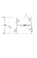
電流が、電磁石10を通って順方向にトランジスタ20aからトランジスタ20bへ、つまり、右から左へ流れる。
その他の場合、ONA =1/2(Nfull−NA +dA )およびdA =−dA
また、OFFA =ONA +NA
ただし、Nfullは、周期カウント(512)の最大数であり、dA は、最初、+1に設定され、その値は、一つの期間から次の期間へ伝えられる。認識されるように、トランジスタ20bに対するエッジ位置は、対応する方法で(例えば、下付き文字「A」と下付き文字「B」と交換することによって)決定する。
Claims (35)
- スイッチング回路であって、+VsのDC信号を受けるように作動可能な入力と、出力と、オンおよびオフ状態の様々な組合せの間のスイッチングが、+Vs、0Vおよび−Vsのレベルでの電圧パルスを伴う電気信号を上記出力において生成するように、オンおよびオフ状態の間でスイッチすべき第1および第2のスイッチング信号に応答して作動可能な第1および第2のスイッチと、上記スイッチング回路における電圧オフセットを示す信号を生成する電圧センサとを備えるスイッチング回路。
- 上記電圧センサは、上記DC信号の変動を測定するように配置される請求項1に記載のスイッチング回路。
- 上記電圧センサは、上記DC信号の予測値を示す信号を生成するために配置される請求項1に記載のスイッチング回路。
- 上記電圧センサは、上記DC信号を測定するために配置された限定インパルス応答フィルタを含む請求項3に記載のスイッチング回路。
- 上記電圧センサは、上記スイッチング回路におけるダイオードおよび/またはトランジスタの両端の電圧降下を示す信号を生成するように作動可能である請求項1乃至4のいずれか一に記載のスイッチング回路。
- 上記電圧センサは、上記出力を通じて流れる電流を測定するために配置される請求項5に記載のスイッチング回路。
- 上記電圧センサは、上記出力を通じて流れる電流の測定、およびダイオードおよび/またはトランジスタの抵抗値を参照して、上記スイッチング回路における上記ダイオードおよび/またはトランジスタの両端の電圧降下を示す信号を生成するように作動可能である請求項6に記載のスイッチング回路。
- 上記スイッチング回路は、電圧+VsのDC信号を受ける入力と、出力と、それぞれ第1および第2のスイッチを有する第1および第2のアームとを有するブリッジ回路を備え、上記第1および第2のアームは、上記出力の対向端部に接続されている請求項1乃至7のいずれか一に記載のスイッチング回路。
- 上記ブリッジ回路は、ダイオードを有する第3および第4のアームを備えたハーフブリッジである請求項8に記載のスイッチング回路。
- 上記第1および第2のスイッチは、トランジスタである請求項8または9に記載のスイッチング回路。
- 上記ブリッジ回路の出力の両端に電磁石が接続される請求項8乃至10のいずれか一に記載のスイッチング回路。
- 上記第1および第2のスイッチング信号をノイズシェープするように作動可能なノイズシェーパをさらに備える請求項1乃至11のいずれか一に記載のスイッチング回路。
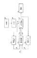
- 電圧+VsのDC信号を受ける入力と、出力と、第1および第2のスイッチとを備えるスイッチング回路を作動させる方法であって、
(a)一つの期間において、上記出力に供給すべき電気信号の所望の電圧を示す電圧要求信号を受ける工程と、
(b)上記電圧要求信号を参照するとともに、上記スイッチング回路の電圧オフセットを参照して、第1および第2のスイッチング信号を生成する工程と、
(c)上記第1および第2のスイッチング信号を、上記期間中にそれぞれ上記第1および第2のスイッチに印加する工程とを備え、
上記スイッチング信号は、上記スイッチを、オンおよびオフ状態の間でスイッチさせ、上記第1および第2のスイッチのオンおよびオフ状態の様々な組合せ間のスイッチングは、+Vs、0Vおよび−Vsのレベルでの電圧パルスによって、上記出力に電気信号を生成し、
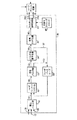
上記第1および第2のスイッチング信号は、上記期間中に上記出力に供給される電気信号の平均電圧が、所望の電圧に実質的に等しいように生成されることを特徴とするスイッチング回路を作動させる方法。 - 上記第1および第2のスイッチング信号のうちの少なくとも一方は、上記DC信号を示す電圧信号を参照して生成され、上記第1または第2のスイッチング信号の少なくとも一方は、上記DC電源の変動を補償する請求項13に記載の方法。
- 上記電圧信号は、上記DC電源の変動の予想測定値を得るためにフィルタを通過される請求項14に記載の方法。
- 上記電圧信号は、限定インパルス応答フィルタを通過される請求項15に記載の方法。
- 上記第1および第2のスイッチング信号のうちの少なくとも一方は、上記スイッチング回路におけるダイオードおよび/またはトランジスタの両端の電圧降下を補償するために生成される請求項13乃至16のいずれか一に記載の方法。
- 上記第1または第2のスイッチング信号の少なくとも一方は、上記出力を通じて流れる電流を示す電流信号および上記ダイオードまたはトランジスタの対応する抵抗を参照して生成される請求項17に記載の方法。
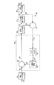
- 上記第1または第2のスイッチング信号の少なくとも一方は、上記第1または第2のスイッチにおける遅い応答時間によって引き起こされる電圧オフセットの測定を参照して生成される請求項13乃至18のいずれか一に記載の方法。
- 上記スイッチング回路は、電圧+VsのDC信号を受ける入力と、出力と、第1および第2のスイッチをそれぞれ有する第1および第2のアームとを有するブリッジ回路を備え、上記第1および第2のアームは、上記出力の対向端部に接続されている請求項13乃至19のいずれか一に記載の方法。
- 上記ブリッジ回路は、ダイオードを有する第3および第4のアームを有するハーフブリッジである請求項20に記載の方法。
- 上記第1および第2のスイッチはトランジスタであり、上記方法は、それぞれ該トランジスタを流れる実質的に最大および実質的に最少の電流に応じて、上記トランジスタをオンおよびオフ状態の間でスイッチングする工程を備える請求項20または21に記載の方法。
- パルス状の第1および第2のスイッチング信号を生成する工程を備える請求項13乃至22のいずれか一に記載の方法。
- 上記第1および第2のスイッチが同時にスイッチされないという規則に従って、上記第1および第2のスイッチング信号を生成する工程を備える請求項24に記載の方法。
- 上記信号が期間毎に2つ以上のパルスを有しないという規則に従って、上記第1および第2のスイッチング信号を生成する工程を備える請求項23または24に記載の方法。
- いずれのパルスも、上記期間の中心に関して対称的に配置すべきであるという規則に従って、上記第1および第2のスイッチング信号を生成する工程を備える請求項25に記載の方法。
- パルスを対称的にセンタリングできない場合には、非対称パルスのより長くかつより短い側が、連続するパルスに対して、立ち上がり側と立ち下がり側との間で交番されるという規則に従って、上記第1および第2のスイッチング信号を生成する工程を備える請求項26に記載の方法。
- パルス幅変調方式に従って、上記第1および第2のスイッチング信号を生成する工程を備える請求項23乃至27のいずれか一に記載の方法。
- 上記第1および第2のスイッチング信号をノイズシェープする工程を備える請求項23乃至28のいずれか一に記載の方法。
- 一つの期間内で、上記出力へ供給すべき所望電流を示す電流要求信号を受けて、上記所望電流に実質的に等しい電流によって上記期間中に上記出力に供給される電気信号をもたらす、上記出力に印加すべき電気信号の所望電圧を示す電圧要求信号を算出する工程を備える請求項13乃至29のいずれか一に記載の方法。
- 上記電圧要求信号を計算する工程は、出力に接続された負荷の負荷特性のモデルを参照して実行される請求項30に記載の方法。
- 上記出力を通じて流れる電流を示す電流信号を参照して上記電圧要求信号を生成する工程をさらに備える請求項30または31に記載の方法。
- コンピュータおよび/または上記スイッチング回路と関連する他の処理手段でコンピュータプログラムが実行されているときに、請求項13乃至32のいずれかに記載の方法工程を実行するプログラムコード手段を備えるコンピュータプログラム。
- コンピュータおよび/または上記スイッチング回路と関連する他の処理手段でコンピュータプログラムが実行されているときに、請求項13乃至22のいずれかに記載の方法工程を実行するコンピュータ読取り可能な媒体に格納されたプログラムコード手段を備えるコンピュータプログラム製品。
- 請求項13乃至32のいずれかに記載の方法工程を実行するためにプログラミングされた処理手段をさらに備える請求項1乃至12のいずれかに記載のスイッチング回路。
Applications Claiming Priority (2)
| Application Number | Priority Date | Filing Date | Title |
|---|---|---|---|
| GBGB0200024.8A GB0200024D0 (en) | 2002-01-02 | 2002-01-02 | A switching circuit and a method of operation thereof |
| PCT/GB2002/005733 WO2003061103A2 (en) | 2002-01-02 | 2002-12-17 | A switching circuit and a method of operation thereof |
Publications (2)
| Publication Number | Publication Date |
|---|---|
| JP2005515744A true JP2005515744A (ja) | 2005-05-26 |
| JP4068568B2 JP4068568B2 (ja) | 2008-03-26 |
Family
ID=9928541
Family Applications (1)
| Application Number | Title | Priority Date | Filing Date |
|---|---|---|---|
| JP2003561076A Expired - Fee Related JP4068568B2 (ja) | 2002-01-02 | 2002-12-17 | スイッチング回路およびその作動方法 |
Country Status (6)
| Country | Link |
|---|---|
| US (1) | US7692337B2 (ja) |
| EP (1) | EP1461856A2 (ja) |
| JP (1) | JP4068568B2 (ja) |
| AU (1) | AU2002352417A1 (ja) |
| GB (1) | GB0200024D0 (ja) |
| WO (1) | WO2003061103A2 (ja) |
Cited By (1)
| Publication number | Priority date | Publication date | Assignee | Title |
|---|---|---|---|---|
| JP2013162544A (ja) * | 2012-02-01 | 2013-08-19 | Nippon Steel & Sumitomo Metal | 電力変換システムの制御方法及び電力変換システム |
Families Citing this family (1)
| Publication number | Priority date | Publication date | Assignee | Title |
|---|---|---|---|---|
| US9048831B2 (en) * | 2012-07-13 | 2015-06-02 | General Electric Company | Systems and methods for regulating semiconductor devices |
Family Cites Families (38)
| Publication number | Priority date | Publication date | Assignee | Title |
|---|---|---|---|---|
| GB2014388B (en) | 1977-10-28 | 1982-05-19 | Ferranti Ltd | Transistor bridge circuit |
| DE3037305C2 (de) | 1980-10-02 | 1986-04-03 | Flowtec AG, Reinach, Basel | Anordnung zur Erzeugung magnetischer Gleichfelder wechselnder Polarität für die magnetisch-induktive Durchflußmessung |
| US4585986A (en) | 1983-11-29 | 1986-04-29 | The United States Of America As Represented By The Department Of Energy | DC switching regulated power supply for driving an inductive load |
| DE3402759A1 (de) | 1984-01-27 | 1985-08-01 | Robert Bosch Gmbh, 7000 Stuttgart | Stromregler fuer elektromagnetische stellantriebe |
| GB8530930D0 (en) | 1985-12-16 | 1986-01-29 | Mansfield P | Inductive circuit arrangements |
| DE3603071A1 (de) | 1986-02-01 | 1987-08-06 | Leybold Heraeus Gmbh & Co Kg | Gleichstrom-wechselstrom-wandler mit asymmetrischer halbbrueckenschaltung |
| DE3638174A1 (de) | 1986-11-08 | 1988-05-19 | Parker Hannifin Nmf Gmbh | Treiberschaltung fuer induktive verbraucher |
| JP2578134B2 (ja) | 1987-10-22 | 1997-02-05 | 白木金属工業株式会社 | ソレノイドの駆動回路 |
| JPH01247507A (ja) | 1988-03-30 | 1989-10-03 | Nippon Steel Corp | 溶融金属の粒滴化方法 |
| US4890188A (en) | 1988-10-04 | 1989-12-26 | Lockwood Technical, Inc. | Solenoid driver system |
| JP2799886B2 (ja) | 1989-09-11 | 1998-09-21 | 株式会社セコー技研 | インダクタンス負荷の通電制御装置 |
| DE4018930C2 (de) | 1990-06-13 | 1994-07-14 | Klug Rolf Dieter Dr Ing | Brückenzweig von Gleichstromstellern und Pulswechselrichtern mit geregeltem Querstrom |
| CA2053540C (en) | 1991-10-11 | 2001-05-15 | Gyula Eisenbart | Inductive load switch utilizing simplified gating |
| JPH0683402A (ja) * | 1992-08-31 | 1994-03-25 | Toshiba Corp | Pwm駆動回路 |
| JP3070355B2 (ja) | 1993-10-06 | 2000-07-31 | トヨタ自動車株式会社 | 自動変速機のソレノイド駆動制御装置 |
| DE4413240A1 (de) | 1994-04-16 | 1995-10-19 | Bosch Gmbh Robert | Vorrichtung und ein Verfahren zur Ansteuerung eines elektromagnetischen Verbrauchers |
| US5559467A (en) * | 1995-01-27 | 1996-09-24 | The Regents Of The University Of California | Digital, pulse width modulation audio power amplifier with noise and ripple shaping |
| DE69523752T2 (de) | 1995-08-31 | 2002-08-29 | St Microelectronics Srl | Verfahren und Schaltung zur pulsbreitenmodulierten Steuerung einer Brücke und eines Plattenantriebs und unter Verwendung derselben |
| JP3108626B2 (ja) | 1996-03-26 | 2000-11-13 | シャープ株式会社 | インバータブリッジのゲート駆動信号発生方法 |
| US5977725A (en) | 1996-09-03 | 1999-11-02 | Hitachi, Ltd. | Resonance type power converter unit, lighting apparatus for illumination using the same and method for control of the converter unit and lighting apparatus |
| JP3758305B2 (ja) | 1996-09-17 | 2006-03-22 | 株式会社日立製作所 | 照明用点灯装置 |
| JP3801273B2 (ja) | 1996-09-20 | 2006-07-26 | カヤバ工業株式会社 | 電磁弁駆動回路 |
| DE19808297A1 (de) | 1997-03-05 | 1998-09-10 | Mannesmann Rexroth Ag | Stromgeregelte Endstufe für elektromagnetische Stellantriebe |
| US5847554A (en) * | 1997-06-13 | 1998-12-08 | Linear Technology Corporation | Synchronous switching regulator which employs switch voltage-drop for current sensing |
| DE19728318C1 (de) | 1997-06-27 | 1999-04-01 | Daimler Benz Ag | Verfahren zur Vermeidung der Sättigung von Einphasentransformatoren durch Gleichflüsse |
| JPH1169629A (ja) | 1997-08-21 | 1999-03-09 | Nissin Electric Co Ltd | アクティブフィルタの制御方法 |
| DE19747033A1 (de) | 1997-10-24 | 1999-04-29 | Daimler Chrysler Ag | Elektronische Schalteinrichtung für Magneten |
| JP3744680B2 (ja) | 1998-03-31 | 2006-02-15 | 富士通株式会社 | 電源装置、および電源回路の制御方法 |
| JP2000006523A (ja) | 1998-06-24 | 2000-01-11 | Dainippon Printing Co Ltd | 熱転写シート及びそれを用いたicカード |
| US6213442B1 (en) | 1998-10-08 | 2001-04-10 | Lord Corporation | Isolation system for isolation tables and the like |
| US6081104A (en) * | 1998-11-20 | 2000-06-27 | Applied Power Corporation | Method and apparatus for providing energy to a lighting system |
| FR2786920B1 (fr) * | 1998-12-07 | 2001-01-12 | Schneider Electric Ind Sa | Dispositif de commande standard d'un electro-aimant d'ouverture ou de fermeture d'un disjoncteur |
| WO2000074222A1 (en) | 1999-05-27 | 2000-12-07 | Hitachi, Ltd. | H-type bridge circuit and integrated circuit |
| EP1081842B1 (en) * | 1999-09-01 | 2004-05-26 | Ramachandran Ramarathnam | A multi-speed motor controller |
| DE50010766D1 (de) | 1999-09-16 | 2005-08-25 | Siemens Ag | Verfahren zum steuern eines elektromechanischen stellantriebes |
| US6577488B1 (en) | 2000-01-14 | 2003-06-10 | Motorola, Inc. | Inductive load driver utilizing energy recovery |
| DE10018175A1 (de) | 2000-04-12 | 2001-10-25 | Bayerische Motoren Werke Ag | Schaltungsanordnung zum Betrieb eines hochdynamischen elektromagnetischen Hubanker-Aktors |
| GB0200027D0 (en) * | 2002-01-02 | 2002-02-13 | Bae Systems Plc | Improvements relating to operation of a current controller |
-
2002
- 2002-01-02 GB GBGB0200024.8A patent/GB0200024D0/en not_active Ceased
- 2002-12-17 EP EP02788137A patent/EP1461856A2/en not_active Withdrawn
- 2002-12-17 WO PCT/GB2002/005733 patent/WO2003061103A2/en not_active Ceased
- 2002-12-17 US US10/500,623 patent/US7692337B2/en not_active Expired - Fee Related
- 2002-12-17 AU AU2002352417A patent/AU2002352417A1/en not_active Abandoned
- 2002-12-17 JP JP2003561076A patent/JP4068568B2/ja not_active Expired - Fee Related
Cited By (1)
| Publication number | Priority date | Publication date | Assignee | Title |
|---|---|---|---|---|
| JP2013162544A (ja) * | 2012-02-01 | 2013-08-19 | Nippon Steel & Sumitomo Metal | 電力変換システムの制御方法及び電力変換システム |
Also Published As
| Publication number | Publication date |
|---|---|
| WO2003061103A2 (en) | 2003-07-24 |
| WO2003061103A3 (en) | 2003-10-16 |
| US7692337B2 (en) | 2010-04-06 |
| EP1461856A2 (en) | 2004-09-29 |
| GB0200024D0 (en) | 2002-02-13 |
| JP4068568B2 (ja) | 2008-03-26 |
| US20050077927A1 (en) | 2005-04-14 |
| AU2002352417A1 (en) | 2003-07-30 |
Similar Documents
| Publication | Publication Date | Title |
|---|---|---|
| CN106688172B (zh) | 用于控制dc-dc转换器的方法 | |
| US7724547B1 (en) | Compensating on-time delay of switching transistor in switching power converters | |
| JP2012221761A (ja) | 除電装置及び除電制御方法 | |
| US7498789B2 (en) | Switching regulator with over-current protection | |
| CN104852568B (zh) | 基于Cuk的电流源 | |
| JP5343229B2 (ja) | インバータ | |
| JP4068569B2 (ja) | スイッチング回路およびその作動方法 | |
| US12237763B2 (en) | Dead time adjusted pulse width modulator | |
| JP4383881B2 (ja) | ブリッジ回路のパルス幅変調制御方法およびブリッジ回路を作動させる方法 | |
| JP4068568B2 (ja) | スイッチング回路およびその作動方法 | |
| JP2002151974A (ja) | パルス幅変調アンプ | |
| RU2326482C2 (ru) | Генератор импульсов | |
| US10862471B2 (en) | Signal modulator | |
| JP4966252B2 (ja) | スイッチング電源装置 | |
| US20230362540A1 (en) | Method of table learning with reduced learning rate applied in driving circuit and driving circuit using the same | |
| US20230291313A1 (en) | Method applied in driving circuit and driving circuit using the same | |
| JP5870708B2 (ja) | Ac−dc変換回路および力率改善方法 | |
| JP4747817B2 (ja) | スイッチタイミング制御回路 | |
| JP6787283B2 (ja) | 力率改善回路及び充電器 | |
| KR102700873B1 (ko) | 구동 회로에 적용되는 전도 손실 및 스위칭 손실 감소 방법 및 이를 사용하는 구동 회로 | |
| KR20150139289A (ko) | 오프신호 발생기 및 그를 포함하는 전원공급장치 | |
| JPH0536523A (ja) | パルス電流供給装置 | |
| KR101714573B1 (ko) | 아날로그 인버터 구동장치 | |
| KR20200002459A (ko) | 전류 제어 장치, 스위칭 소자 제어 장치 및 밸브 장치 | |
| US20200235685A1 (en) | Actuator driving device |
Legal Events
| Date | Code | Title | Description |
|---|---|---|---|
| A131 | Notification of reasons for refusal |
Free format text: JAPANESE INTERMEDIATE CODE: A131 Effective date: 20061024 |
|
| A601 | Written request for extension of time |
Free format text: JAPANESE INTERMEDIATE CODE: A601 Effective date: 20070117 |
|
| A602 | Written permission of extension of time |
Free format text: JAPANESE INTERMEDIATE CODE: A602 Effective date: 20070125 |
|
| A521 | Request for written amendment filed |
Free format text: JAPANESE INTERMEDIATE CODE: A523 Effective date: 20070416 |
|
| A131 | Notification of reasons for refusal |
Free format text: JAPANESE INTERMEDIATE CODE: A131 Effective date: 20070522 |
|
| A601 | Written request for extension of time |
Free format text: JAPANESE INTERMEDIATE CODE: A601 Effective date: 20070815 |
|
| A602 | Written permission of extension of time |
Free format text: JAPANESE INTERMEDIATE CODE: A602 Effective date: 20070822 |
|
| TRDD | Decision of grant or rejection written | ||
| A01 | Written decision to grant a patent or to grant a registration (utility model) |
Free format text: JAPANESE INTERMEDIATE CODE: A01 Effective date: 20071211 |
|
| A61 | First payment of annual fees (during grant procedure) |
Free format text: JAPANESE INTERMEDIATE CODE: A61 Effective date: 20080110 |
|
| FPAY | Renewal fee payment (event date is renewal date of database) |
Free format text: PAYMENT UNTIL: 20110118 Year of fee payment: 3 |
|
| R150 | Certificate of patent or registration of utility model |
Free format text: JAPANESE INTERMEDIATE CODE: R150 |
|
| LAPS | Cancellation because of no payment of annual fees |