JP2005515744A - Switching circuit and operating method thereof - Google Patents
Switching circuit and operating method thereof Download PDFInfo
- Publication number
- JP2005515744A JP2005515744A JP2003561076A JP2003561076A JP2005515744A JP 2005515744 A JP2005515744 A JP 2005515744A JP 2003561076 A JP2003561076 A JP 2003561076A JP 2003561076 A JP2003561076 A JP 2003561076A JP 2005515744 A JP2005515744 A JP 2005515744A
- Authority
- JP
- Japan
- Prior art keywords
- voltage
- signal
- switching
- switching circuit
- output
- Prior art date
- Legal status (The legal status is an assumption and is not a legal conclusion. Google has not performed a legal analysis and makes no representation as to the accuracy of the status listed.)
- Granted
Links
Images


Classifications
-
- H—ELECTRICITY
- H02—GENERATION; CONVERSION OR DISTRIBUTION OF ELECTRIC POWER
- H02M—APPARATUS FOR CONVERSION BETWEEN AC AND AC, BETWEEN AC AND DC, OR BETWEEN DC AND DC, AND FOR USE WITH MAINS OR SIMILAR POWER SUPPLY SYSTEMS; CONVERSION OF DC OR AC INPUT POWER INTO SURGE OUTPUT POWER; CONTROL OR REGULATION THEREOF
- H02M3/00—Conversion of DC power input into DC power output
- H02M3/02—Conversion of DC power input into DC power output without intermediate conversion into AC
- H02M3/04—Conversion of DC power input into DC power output without intermediate conversion into AC by static converters
- H02M3/10—Conversion of DC power input into DC power output without intermediate conversion into AC by static converters using discharge tubes with control electrode or semiconductor devices with control electrode
- H02M3/145—Conversion of DC power input into DC power output without intermediate conversion into AC by static converters using discharge tubes with control electrode or semiconductor devices with control electrode using devices of a triode or transistor type requiring continuous application of a control signal
- H02M3/155—Conversion of DC power input into DC power output without intermediate conversion into AC by static converters using discharge tubes with control electrode or semiconductor devices with control electrode using devices of a triode or transistor type requiring continuous application of a control signal using semiconductor devices only
- H02M3/156—Conversion of DC power input into DC power output without intermediate conversion into AC by static converters using discharge tubes with control electrode or semiconductor devices with control electrode using devices of a triode or transistor type requiring continuous application of a control signal using semiconductor devices only with automatic control of output voltage or current, e.g. switching regulators
- H02M3/158—Conversion of DC power input into DC power output without intermediate conversion into AC by static converters using discharge tubes with control electrode or semiconductor devices with control electrode using devices of a triode or transistor type requiring continuous application of a control signal using semiconductor devices only with automatic control of output voltage or current, e.g. switching regulators including plural semiconductor devices as final control devices for a single load
Landscapes
- Engineering & Computer Science (AREA)
- Power Engineering (AREA)
- Relay Circuits (AREA)
- Dc-Dc Converters (AREA)
- Electronic Switches (AREA)
Abstract
本発明は、スイッチング回路の出力において、ある電圧で電気信号を生成することが可能な第1および第2のスイッチを備えるブリッジ回路のようなスイッチング回路に関する。また、本発明は、このようなスイッチング回路の作動方法に関する。このスイッチング回路は、+VsのDC信号を受けるように作動可能な入力と、出力と、オンおよびオフ状態の様々な組合せの間のスイッチングが、+Vs、0Vおよび−Vsのレベルでの電圧パルスを伴う電気信号を該出力で生成するように、オンおよびオフ状態の間でスイッチングされる第1および第2のスイッチング信号に応答して作動可能な第1および第2のスイッチと、該スイッチング回路における電圧オフセットを示す信号を生成する電圧センサとを備える。このスイッチング回路における電圧の影響は、上記電圧センサによって生成される信号を用いることによって補償することができる。 The present invention relates to a switching circuit such as a bridge circuit including first and second switches capable of generating an electrical signal at a certain voltage at the output of the switching circuit. The invention also relates to a method for operating such a switching circuit. This switching circuit switches between various combinations of inputs, outputs, and on and off states that are operable to receive a + Vs DC signal, with voltage pulses at levels of + Vs, 0V, and −Vs. First and second switches operable in response to first and second switching signals switched between on and off states to generate an electrical signal at the output, and a voltage at the switching circuit And a voltage sensor that generates a signal indicating an offset. The influence of the voltage in the switching circuit can be compensated by using a signal generated by the voltage sensor.
Description
本発明は、スイッチング回路の出力において、ある電圧で電気信号を生成することが可能な第1および第2のスイッチを備えるスイッチング回路に関する。また、本発明は、このようなスイッチング回路の作動方法に関する。 The present invention relates to a switching circuit including first and second switches capable of generating an electrical signal at a certain voltage at the output of the switching circuit. The invention also relates to a method for operating such a switching circuit.
上記スイッチング回路は、要求された電圧に従って、ブリッジ回路の出力に接続された負荷の両端に電圧を生成するように作動するブリッジ回路を備える。例えば、本発明の現在意図されている用途は、非常に高い公差を満たさなければならない、電磁石によって生じた要求される力に応答して該電磁石を駆動する場合である。該電磁石によって生じた力は、電流または電圧の制御は、該電磁石によって生じる力に影響を及ぼすため、電流要求または電圧要求のいずれかに応答して制御することができる。また、電流コントローラは、力要求に応答して作動させることができるが、このことは、電流または電圧要求に変換しなければならない。要求された電圧を上記電磁石の両端に設定している状態で、該電流コントローラが、電圧要求モードで作動している場合でも、このことは、当然、該電磁石を通って流れる電流に影響を及ぼすことになるため、用語「電流コントローラ」は、電圧または電流または電界要求に応答する動作をカバーするのに用いられる。 The switching circuit includes a bridge circuit that operates to generate a voltage across a load connected to the output of the bridge circuit according to a required voltage. For example, the presently contemplated application of the present invention is where the electromagnet is driven in response to the required force generated by the electromagnet that must meet very high tolerances. The force generated by the electromagnet can be controlled in response to either a current request or a voltage request because the control of the current or voltage affects the force generated by the electromagnet. The current controller can also be activated in response to force demands, which must be converted into current or voltage demands. This naturally affects the current flowing through the electromagnet, even when the current controller is operating in voltage demand mode with the required voltage set across the electromagnet. As such, the term “current controller” is used to cover operations that respond to voltage or current or electric field demands.
上記電流コントローラが、電圧要求に応答して作動する場合、電磁石に関連する大きなインダクタンスが、該電磁石の両端に印加される平均電圧におけるドリフトに円滑に追従するような該電流の遅い応答時間につながるため、高周波電圧パルスを該電磁石に印加してもよい。 When the current controller operates in response to a voltage demand, the large inductance associated with the electromagnet leads to a slow response time for the current so that it smoothly follows the drift in the average voltage applied across the electromagnet. Therefore, a high frequency voltage pulse may be applied to the electromagnet.
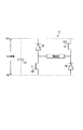
公知のスイッチング回路を図1に示す。図を見て分かるように、該スイッチング回路は、一つの電磁石を、その出力の両端に接続した電磁石を有するハーフブリッジを備える。該電磁石の両端電圧の制御は、該ブリッジ回路の対向するアームに配置された一対のトランジスタをスイッチングして(他方の対向アームは、上記ハーフブリッジ回路を完成させるためにダイオードを含んでいる)、+Vsと−Vsとの間で上記電磁石の両端電圧の極性を交番することによって実施される。電流または電圧要求が受け入れられて、この要求に合わせるためにスイッチング信号が生成される。このスイッチング信号は、符号AおよびBで示される箇所に供給されて、上記トランジスタが、最大および最少導通状態間でスイッチングされるように該トランジスタを制御する(該トランジスタの線型領域は、電力効率が悪いために用いられない)。上記ハーフブリッジ回路のダイオードは、電流が、上記電磁石のみを通って、この場合、図1における右から左への一方向に流れることを保証する。上記電流コントローラは、両トランジスタがオンし(例えば、導通し)、+Vsの電圧が上記電磁石の両端に印加され、また、上記トランジスタがオフし(例えば、非導通であり)、−Vsの電圧が該電磁石の両端に印加されたときに、該トランジスタが同時にスイッチングされるように作動される。+Vsおよび−Vsにおけるデューティサイクルは、その期間において上記電磁石へ供給される平均電流を決定するが、該電磁石のインダクタンスというものは、電流が各電圧パルスと鋭敏に一致するよりもむしろ、電圧に円滑に追従することを保証するものであるということを思い起こす。すなわち、上記トランジスタを適切な時刻にスイッチングすることにより、所望の電流を上記電磁石へ供給することができる。DC電源に戻すことができない、上記電磁石から引っ張られた電流を保持するために、リザーバキャパシタが含まれている。 A known switching circuit is shown in FIG. As can be seen from the figure, the switching circuit comprises a half bridge having an electromagnet with one electromagnet connected to both ends of its output. Control of the voltage across the electromagnet switches a pair of transistors located on opposing arms of the bridge circuit (the other opposing arm contains a diode to complete the half-bridge circuit) This is done by alternating the polarity of the voltage across the electromagnet between + Vs and -Vs. A current or voltage request is accepted and a switching signal is generated to meet this request. This switching signal is supplied to the locations indicated by symbols A and B to control the transistor so that the transistor is switched between maximum and minimum conduction states (the linear region of the transistor is power efficient). Not used because of bad). The diode of the half-bridge circuit ensures that current flows only through the electromagnet, in this case in one direction from right to left in FIG. In the current controller, both transistors are turned on (for example, conductive), a voltage of + Vs is applied across the electromagnet, the transistor is turned off (for example, non-conductive), and a voltage of −Vs is When applied across the electromagnet, the transistors are actuated to be switched simultaneously. The duty cycle at + Vs and -Vs determines the average current supplied to the electromagnet during that period, but the electromagnet's inductance is smooth to the voltage rather than the current closely matching each voltage pulse. Recall that it is a guarantee of following. In other words, a desired current can be supplied to the electromagnet by switching the transistor at an appropriate time. A reservoir capacitor is included to hold the current drawn from the electromagnet that cannot be returned to the DC power source.
これらのデューティサイクルを生成するパルス電圧信号は、上記トランジスタに供給されるパルススイッチング信号を用いて実施される。該スイッチング信号は、アナログ実施機構によるパルス幅変調構成に従って変調され、その結果、一期間内の該パルス幅は、+Vsでのパルスが、−Vsでの残りの時間に対して変化して、所望の電流を生成するように変化する。別法として、従来よく知られているように、パルス密度変調構成を用いてもよい。 The pulse voltage signal that generates these duty cycles is implemented using a pulse switching signal supplied to the transistor. The switching signal is modulated according to a pulse width modulation configuration by an analog implementation mechanism, so that the pulse width within a period is changed as desired by changing the pulse at + Vs to the remaining time at -Vs. To produce a current of. Alternatively, a pulse density modulation configuration may be used, as is well known in the art.
上述したスイッチング回路に伴う問題は、該回路の様々なパーツの両端電圧には、上記電磁石の両端で生成された電圧を、所望の電圧と異ならせる若干のオフセットがあるということである。これらの電圧オフセットは、(電力供給によるリプルおよび、特に上記リザーバキャパシタが充放電するときに変化する該リザーバキャパシタの両端電圧により)+Vs程度の公称値のDC電源の変動によって、および、上記ダイオードおよびトランジスタの固有抵抗によって生じる該ダイオードおよびトランジスタの両端の電圧の降下によって生じる可能性がある。また、構成素子の遅い応答時間は、所望の変化に遅れる、上記電磁石に供給される電圧の遅い変化を引き起こす。これらの影響が修正されない場合、その期間中に上記電磁石に供給される平均電圧は、要求される電圧に合わないであろう。 The problem with the switching circuit described above is that the voltage across the various parts of the circuit has a slight offset that makes the voltage generated across the electromagnet different from the desired voltage. These voltage offsets are due to fluctuations in the nominal DC power supply on the order of + Vs (due to ripple due to power supply and in particular the voltage across the reservoir capacitor that changes when the reservoir capacitor charges and discharges) and the diode and It can be caused by a drop in voltage across the diode and transistor caused by the intrinsic resistance of the transistor. Also, the slow response time of the components causes a slow change in the voltage supplied to the electromagnet that is delayed by the desired change. If these effects are not corrected, the average voltage supplied to the electromagnet during that period will not match the required voltage.
第1の態様から、本発明は、+VsのDC信号を受けるように作動可能な入力と、出力と、オンおよびオフ状態の様々な組合せの間のスイッチングが、+Vs、0Vおよび−Vsのレベルでの電圧パルスを伴う電気信号を該出力で生成するように、オンおよびオフ状態の間でスイッチングされる第1および第2のスイッチング信号に応答して作動可能な第1および第2のスイッチと、スイッチング回路における電圧オフセットを示す信号を生成する電圧センサとを備えるスイッチング回路に存する。 From the first aspect, the present invention provides switching between various combinations of input, output, and on and off states operable to receive a + Vs DC signal at levels of + Vs, 0V and −Vs. First and second switches operable in response to first and second switching signals switched between on and off states to generate an electrical signal with a voltage pulse of The switching circuit includes a voltage sensor that generates a signal indicating a voltage offset in the switching circuit.
上記電圧センサを用いて上記スイッチング回路における電圧オフセットを示す信号を生成することにより、該スイッチング回路における電圧の影響を補償することができる。上記電圧センサが測定または判断する情報は、上記スイッチング回路の使用に従って、および該スイッチング回路に接続されているものに従って変化してもよい。 By generating a signal indicating a voltage offset in the switching circuit using the voltage sensor, the influence of the voltage in the switching circuit can be compensated. The information measured or determined by the voltage sensor may vary according to the use of the switching circuit and according to what is connected to the switching circuit.
任意に、上記電圧センサは、上記DC信号の変動を測定するように配置される。上記DC電源の測定されたいかなる変動も、3つのレベル+Vs、0Vおよび−Vsにおける上記出力の相対的なデューティサイクルを調整することによって補償することができる。このことは、上記DC電源自体の測定値を用いることにより、あるいは、該DC電源の公称電圧+Vsからのずれの測定値を用いることにより実施することができる。 Optionally, the voltage sensor is arranged to measure fluctuations in the DC signal. Any measured variation of the DC power supply can be compensated for by adjusting the relative duty cycle of the output at three levels + Vs, 0V and −Vs. This can be done by using the measured value of the DC power supply itself, or by using a measured value of deviation from the nominal voltage + Vs of the DC power supply.
有利には、上記電圧センサは、上記DC信号の予測値を示す信号を生成するために配置してもよい。このことは、上記電圧センサの遅延が、上記スイッチング回路の上記DC電源の変動に対する応答における容認できない遅れにつながる場合に、特に有用である。適切には、該電圧センサは、該DC信号を測定するために配置された限定インパルス応答フィルタを含む。 Advantageously, the voltage sensor may be arranged to generate a signal indicative of the predicted value of the DC signal. This is particularly useful when the voltage sensor delay leads to an unacceptable delay in the response of the switching circuit to the DC power supply variations. Suitably, the voltage sensor includes a limited impulse response filter arranged to measure the DC signal.
好ましくは、上記電圧センサは、上記スイッチング回路におけるダイオードおよび/またはトランジスタの両端の電圧降下を示す信号を生成するように作動可能である。このような電圧降下は、所望の電圧から離れた上記出力に供給される電圧の不一致につながる可能性がある。 Preferably, the voltage sensor is operable to generate a signal indicative of a voltage drop across a diode and / or transistor in the switching circuit. Such a voltage drop can lead to a mismatch in the voltage supplied to the output away from the desired voltage.
便利には、上記電圧センサは、上記出力を通じて流れる電流を測定するために配置してもよく、また任意に、該電圧センサは、該出力を通じて流れる電流の測定、およびダイオードおよび/またはトランジスタの抵抗値に関して、上記スイッチング回路における上記ダイオードおよび/またはトランジスタの両端の電圧降下を示す信号を生成するように作動可能であってもよい。このことは、当然、公知のオームの法則の関係、すなわちV=IRを用いることであり、また、上記ダイオードまたはトランジスタを流れる電流を反映する、該ダイオードまたはトランジスタの両端の電圧降下の測定を可能にする。この精度が必要ない場合、上記電圧センサは、その時に該ダイオードまたはトランジスタを通って流れる電流に関係なく、該ダイオードまたはトランジスタに対して対応する電圧降下を単に生成してもよい。 Conveniently, the voltage sensor may be arranged to measure the current flowing through the output, and optionally the voltage sensor measures the current flowing through the output, and the resistance of the diode and / or transistor. In terms of value, it may be operable to generate a signal indicative of a voltage drop across the diode and / or transistor in the switching circuit. This is, of course, using the well-known Ohm's law relationship, ie V = IR, and also allows the measurement of the voltage drop across the diode or transistor reflecting the current through the diode or transistor. To. If this accuracy is not required, the voltage sensor may simply generate a corresponding voltage drop across the diode or transistor, regardless of the current flowing through the diode or transistor at that time.
任意に、上記スイッチング回路は、電圧+VsのDC信号を受ける入力と、出力と、それぞれ第1および第2のスイッチを有する第1および第2のアームとを有するブリッジ回路を備え、該第1および第2のアームは、該出力の対向端部に接続されている。 Optionally, the switching circuit comprises a bridge circuit having an input for receiving a DC signal of voltage + Vs, an output, and first and second arms having first and second switches, respectively. The second arm is connected to the opposite end of the output.
適切には、上記ブリッジ回路は、ダイオードを有する第3および第4のアームを備えたハーフブリッジであってもよい。有利には、上記第1および第2のスイッチは、トランジスタであってもよく、また、任意に、該ブリッジ回路の出力の両端に電磁石を接続してもよい。 Suitably, the bridge circuit may be a half bridge with third and fourth arms having diodes. Advantageously, the first and second switches may be transistors and optionally an electromagnet may be connected across the output of the bridge circuit.
任意に、上記スイッチング回路は、上記第1および第2のスイッチング信号をノイズシェープするように作動可能なノイズシェーパをさらに備えてもよい。このことは、上記スイッチング回路が、量子化ノイズを生じるディジタルスイッチング機構に従って作動される場合に有益である。このノイズは、PWM量子化機構における最も近い利用可能な幅に割り当てられた最適な幅を有しなければならない上記スイッチング信号のパルス性によって生じる。上記最適な幅と最も近い利用可能な幅との間のほとんど避けられない差は量子化誤差であり、それは、該スイッチング回路の出力に供給される電圧に見られる量子化ノイズを形成する連続的な量子化誤差である。ノイズシェーパを含むことは、第1および第2のスイッチング信号における、従って、出力に供給される信号における、量子化ノイズを低減するという点で、非常に有利である。ノイズシェーピングは、当該周波数においてノイズの抑制があるように、上記出力信号のノイズスペクトルをシェーピングすることによって実施される。この効果は、当該帯域の外側の他の周波数における増加したノイズを犠牲にして実現される。 Optionally, the switching circuit may further comprise a noise shaper operable to noise shape the first and second switching signals. This is beneficial when the switching circuit is operated according to a digital switching mechanism that produces quantization noise. This noise is caused by the pulsing nature of the switching signal, which must have an optimum width assigned to the nearest available width in the PWM quantization mechanism. The almost inevitable difference between the optimal width and the nearest available width is the quantization error, which is a continuous noise that forms the quantization noise seen in the voltage supplied to the output of the switching circuit. Quantization error. Including a noise shaper is very advantageous in that it reduces quantization noise in the first and second switching signals, and thus in the signal supplied to the output. Noise shaping is performed by shaping the noise spectrum of the output signal so that there is noise suppression at that frequency. This effect is realized at the expense of increased noise at other frequencies outside the band.
有利には、上記ノイズシェーパは、2次ノイズシェーパ、例えば、直前の2つの期間における量子化誤差を補正するノイズシェーパであってもよい。 Advantageously, the noise shaper may be a secondary noise shaper, for example a noise shaper that corrects quantization errors in the last two periods.
第2の態様によれば、本発明は、電圧+VsのDC信号を受ける入力と、その両端に接続された電磁石を有する出力と、第1および第2のスイッチをそれぞれ有する第1および第2のアームであって、上記電磁石の対向端部に接続されている第1および第2のアームとを備えるブリッジ回路を作動させる方法であって、(a)一つの期間において、該電磁石に供給すべき電気信号の所望の電圧を示す電圧要求信号を受ける工程と、(b)上記電圧要求信号に関して、第1および第2のスイッチング信号を生成する工程と、(c)上記第1および第2のスイッチング信号を、上記期間中にそれぞれ上記第1および第2のスイッチに印加する工程とを備える方法に存する。該スイッチング信号は、上記スイッチを、オンおよびオフ状態の間で切り替えさせ、上記第1および第2のスイッチのオンおよびオフ状態の様々な組合せ間のスイッチングは、+Vs、0Vおよび−Vsのレベルでの電圧パルスによって、上記電磁石の両端に電気信号を生成する。上記第1および第2のスイッチング信号は、上記期間中に上記電磁石に供給される電気信号の平均電圧が、所望の電圧に実質的に等しいように生成される。 According to the second aspect, the present invention provides first and second inputs each having an input receiving a DC signal of voltage + Vs, an output having electromagnets connected to both ends thereof, and first and second switches, respectively. A method of operating a bridge circuit comprising an arm and first and second arms connected to opposite ends of the electromagnet, wherein: (a) to be supplied to the electromagnet in one period Receiving a voltage request signal indicative of a desired voltage of the electrical signal; (b) generating first and second switching signals for the voltage request signal; and (c) the first and second switching. Applying a signal to the first and second switches, respectively, during the period. The switching signal causes the switch to switch between on and off states, and switching between various combinations of the on and off states of the first and second switches is at levels of + Vs, 0V and −Vs. An electric signal is generated at both ends of the electromagnet by the voltage pulse. The first and second switching signals are generated such that the average voltage of the electrical signal supplied to the electromagnet during the period is substantially equal to the desired voltage.
+Vs、0Vおよび−Vsのレベルでのパルスを用いることにより、上記期間中に、+Vs〜−Vsの平均電圧を生成することが可能になる。例えば、0.5Vsの電圧が必要な場合、+Vsの電圧を、上記期間の半期に上記電磁石に、また0Vの電圧を残りの半期に印加することができる。 By using pulses at levels of + Vs, 0V and −Vs, it is possible to generate an average voltage of + Vs to −Vs during the period. For example, when a voltage of 0.5 Vs is required, a voltage of + Vs can be applied to the electromagnet during the half of the period and a voltage of 0 V can be applied during the remaining half.
また、上記電磁石の両端に印加される電圧の制御は、その期間に該電磁石を流れる平均電流を制御する。該電磁石を流れる平均電流は、該電磁石の両端の電圧および上記回路の構成素子(例えば、該電磁石のインダクタンス、該回路のキャパシタンス)に従って変化する。一般に、+Vsの電圧は正の電流を与え、0Vの電圧に対するスイッチングは、徐々にゼロまたは負の値に減少する電流をもたらし、−Vsに対するスイッチングは、急速にゼロまたは負の値に減少する電流をもたらす。フルブリッジ回路を使用した場合、電流は、上記電磁石を介して両方の方向(例えば、正および負の電流)で流れることができ、ハーフブリッジを使用した場合には、該電磁石を通る一方向の電流のみが可能である。 The voltage applied to both ends of the electromagnet controls the average current flowing through the electromagnet during that period. The average current flowing through the electromagnet varies according to the voltage across the electromagnet and the components of the circuit (eg, inductance of the electromagnet, capacitance of the circuit). In general, a voltage of + Vs gives a positive current, switching to a voltage of 0V results in a current that gradually decreases to zero or negative values, and switching to -Vs is a current that rapidly decreases to zero or negative values. Bring. When using a full-bridge circuit, current can flow in both directions (eg, positive and negative current) through the electromagnet, and when using a half-bridge, the current in one direction through the electromagnet Only current is possible.
上記電磁石によって見られる電圧は、以下に示すように、上記第1および第2のスイッチの状態に依存する。両スイッチがオンの場合、該電磁石は、+Vsの電圧を示す。両スイッチがオフの場合には、該電磁石は、−Vsの電圧を示す。そして、一方のスイッチがオンで、他方のスイッチがオフの場合には、どの方向に発展するかに関係なく、上記電磁石は0Vの電圧を示す。 The voltage seen by the electromagnet depends on the state of the first and second switches, as shown below. When both switches are on, the electromagnet exhibits a voltage of + Vs. When both switches are off, the electromagnet exhibits a voltage of -Vs. When one switch is on and the other switch is off, the electromagnet exhibits a voltage of 0 V regardless of the direction of development.
バイポーラスイッチング、例えば、3つの電圧レベル+Vs、0Vおよび−Vsの間のスイッチングは、ユニポーラスイッチング、例えば、+Vs、−Vsのみの間のスイッチングを用いる従来のコントローラよりも有利である。例えば、追加的な1ビットの解像度は、Vsの電圧降下は、ユニポーラスイッチングで得られた2Vsの電圧降下よりも可能であるので、所定のタイミングクロック周波数に対してバイポーラスイッチングを用いて得られる。別法として、同じ解像度は、半分のタイミングクロック周波数のみを用いて得ることもできる。 Bipolar switching, eg, switching between three voltage levels + Vs, 0V and −Vs, is advantageous over conventional controllers that use unipolar switching, eg, switching between + Vs and −Vs only. For example, an additional 1-bit resolution can be obtained using bipolar switching for a given timing clock frequency because the Vs voltage drop is more possible than the 2 Vs voltage drop obtained with unipolar switching. Alternatively, the same resolution can be obtained using only half the timing clock frequency.
好ましくは、上記第1および/または第2のスイッチング信号のパルス幅は、該パルス幅が、上記DC電源の変動を補償するように、該DC信号を示す電圧信号に関して生成される。該DC電源の電圧変動は、それ自体を、上記電磁石によって示される電圧のパルス増幅変調として表わすため、所望の電圧は、期間中に電磁石によって示される平均電圧によって達せられない。上記第1および/または第2のスイッチング信号のパルスに幅を加えることによりまたは該パルスから幅を減ずることにより、失われたまたは増幅した振幅は、上記電磁石によって示される電圧パルスの幅を調整することによって補償することができる。 Preferably, the pulse width of the first and / or second switching signal is generated with respect to a voltage signal indicative of the DC signal such that the pulse width compensates for variations in the DC power supply. Since the voltage variation of the DC power supply represents itself as a pulse amplification modulation of the voltage exhibited by the electromagnet, the desired voltage cannot be reached by the average voltage exhibited by the electromagnet during the period. By adding or subtracting a width to the pulse of the first and / or second switching signal, the lost or amplified amplitude adjusts the width of the voltage pulse indicated by the electromagnet. Can be compensated.
任意に、上記電圧信号は、上記DC電源の変動の予想測定値を得るフィルタを通過する。このことは、上記電圧信号を中継する際の限定された応答時間の問題、および連続する期間中に上記スイッチング信号を生成する際の問題を軽減する。該電圧信号は、限定インパルス応答フィルタを通過してもよい。 Optionally, the voltage signal passes through a filter that obtains an expected measurement of the DC power supply variation. This alleviates the limited response time problem when relaying the voltage signal and the problem of generating the switching signal during successive periods. The voltage signal may pass through a limited impulse response filter.
上記第1または第2のスイッチング信号のパルス幅は、上記ブリッジ回路におけるダイオードおよび/またはトランジスタの両端の電圧降下を補償するために、幅の追加を含むように生成してもよい。適切には、幅の追加は、上記電磁石を流れる電流を示す電流信号および上記ダイオードまたはトランジスタの対応する抵抗に関して計算してもよい。これらの電圧降下が補償されない場合、該電磁石によって示される電圧は、所望の電圧よりも小さくなる。 The pulse width of the first or second switching signal may be generated to include an additional width to compensate for voltage drops across the diodes and / or transistors in the bridge circuit. Suitably, the width addition may be calculated with respect to a current signal indicative of the current flowing through the electromagnet and the corresponding resistance of the diode or transistor. If these voltage drops are not compensated, the voltage exhibited by the electromagnet will be less than the desired voltage.
任意に、上記第1または第2のスイッチング信号のパルス幅は、上記第1または第2のスイッチにおける遅い応答時間によって引き起こされる電圧オフセットを補償するために、追加的な幅を含むように生成される。上記スイッチの応答の遅さは、上記電磁石に供給される電圧に見られるパルスの傾斜する立ち上がりおよび立ち下がりにつながる。該傾斜が等しくない場合、上記期間中に該電磁石に供給される平均電圧は、所望の電圧に合わないであろう。 Optionally, the pulse width of the first or second switching signal is generated to include an additional width to compensate for a voltage offset caused by a slow response time in the first or second switch. The The slow response of the switch leads to the ramping rise and fall of the pulse seen in the voltage supplied to the electromagnet. If the slopes are not equal, the average voltage supplied to the electromagnet during the period will not match the desired voltage.
好ましくは、上記スイッチング回路は、電圧+VsのDC信号を受ける入力と、出力と、第1および第2のスイッチをそれぞれ有する第1および第2のアームとを有するブリッジ回路を備え、該第1および第2のアームは、該出力の対向端部に接続されている。有利には、該ブリッジ回路は、ダイオードを有する第3および第4のアームを有するハーフブリッジであってもよい。任意に、上記第1および第2のスイッチはトランジスタでもよく、上記方法は、それぞれ該トランジスタを流れる実質的に最大および実質的に最少の電流に応じて、該トランジスタをオン状態とオフ状態との間で切り替える工程を備える。該トランジスタは、例えば、MOSFETトランジスタであってもよい。 Preferably, the switching circuit includes a bridge circuit having an input for receiving a DC signal of voltage + Vs, an output, and first and second arms having first and second switches, respectively. The second arm is connected to the opposite end of the output. Advantageously, the bridge circuit may be a half bridge having third and fourth arms with diodes. Optionally, the first and second switches may be transistors, and the method causes the transistor to turn on and off in response to a substantially maximum and substantially minimum current flowing through the transistor, respectively. A step of switching between them. The transistor may be a MOSFET transistor, for example.
任意に、上記方法は、パルス状の第1および第2のスイッチング信号を生成する工程を備えてもよい。このことは、全てディジタルの実装を可能にするので有利である。パルス状スイッチング信号の使用は、上記電磁石の両端に生じる電圧もパルス状であることを意味するが、0Vベースラインに対して+Vsおよび−Vsのパルスがある。 Optionally, the method may comprise the step of generating pulsed first and second switching signals. This is advantageous because it allows an all-digital implementation. The use of a pulsed switching signal means that the voltage generated across the electromagnet is also pulsed, but there are + Vs and -Vs pulses relative to the 0V baseline.
別法として、信号がしきい値を越えたときに行われる上記トランジスタのスイッチングに対して、連続的に変化する信号を用いることができる。このことは、一部がアナログの実装を可能にする。 Alternatively, a continuously changing signal can be used for the transistor switching performed when the signal exceeds a threshold. This allows some analog implementation.
好ましくは、上記方法は、上記第1および第2のスイッチは、同時に切り替えられないという規則に従って、上記第1および第2のパルス状スイッチング信号を生成する工程を備える。一度に1つのみのスイッチを作動させることは、上記電磁石の両端に生じる電圧降下を、各スイッチング発生時に半減させることができるので有利である。このことは、従来の電流コントローラに伴って発生する2Vsの電圧降下が、上記電磁石の絶縁破壊電圧以上かまたは該絶縁破壊電圧に近い場合に特に有利である。逆に、バイポーラスイッチングを採用すると、上記トランジスタをスイッチングするときに、絶縁破壊の恐れなく、上記ブリッジ回路を高電圧DC源から作動させることができる。さらに、パルス繰り返し周波数の高調波における出力波形中の好ましくない成分の電力が、固定された高いレベルから低いレベルに低減され、これは、上記信号が低下したときに低下する。 Preferably, the method comprises the step of generating the first and second pulsed switching signals according to a rule that the first and second switches are not switched simultaneously. Operating only one switch at a time is advantageous because the voltage drop across the electromagnet can be halved at each switching occurrence. This is particularly advantageous when the voltage drop of 2 Vs generated with a conventional current controller is greater than or near the breakdown voltage of the electromagnet. Conversely, when bipolar switching is employed, the bridge circuit can be operated from a high voltage DC source without fear of dielectric breakdown when switching the transistor. Furthermore, the power of undesirable components in the output waveform at the harmonics of the pulse repetition frequency is reduced from a fixed high level to a low level, which decreases when the signal drops.
上記方法は、上記信号が、期間毎に2つ以上のパルスを有しないという規則に従って、上記第1および第2のスイッチング信号を生成する工程を備えてもよい。有利には、このことは、上記スイッチを切り替えなければならない回数を最少化し、それにより電力損失を低減する。 The method may comprise generating the first and second switching signals according to a rule that the signal does not have more than one pulse per period. Advantageously, this minimizes the number of times that the switch must be switched, thereby reducing power loss.
好ましくは、上記方法は、どのパルスも、期間の中心に関して対称的に配置すべきであるという規則に従って、上記第1および第2のスイッチング信号を生成する工程を備えてもよい。これは、いわゆる均一パルス幅変調であり、上記期間の中心に関して対称的である電圧を示す電磁石をもたらす。立ち上がりまたは立ち下がりパルス幅変調等の他の形態のパルス幅変調が可能である。 Preferably, the method may comprise generating the first and second switching signals according to a rule that every pulse should be arranged symmetrically with respect to the center of the period. This is so-called uniform pulse width modulation, resulting in an electromagnet that exhibits a voltage that is symmetric about the center of the period. Other forms of pulse width modulation are possible, such as rising or falling pulse width modulation.
任意に、上記方法は、パルスを対称的にセンタリングできない場合には、非対称パルスのより長くかつより短い側が、連続するパルスに対して、立ち上がり側と立ち下がり側との間で交番されるという規則に従って、上記第1および第2のスイッチング信号を生成する工程を備えてもよい。例えば、一つの期間が、偶数のタイミングクロックサイクルを超えて伸びた場合、奇数のクロックサイクルを占めるパルスは、該期間内で対称的に生成することができず、一方のクロックサイクルは、別の対称的なパルスの立ち上がりまたは立ち下がりに付加しなければならない。本願明細書中で定義した上記方法を実行することにより、ノイズが抑制され、これは、常に立ち上がりに、または常に立ち下り側に重みを付加することによって生じるものではない。 Optionally, the above method is such that if the pulse cannot be symmetrically centered, the longer and shorter sides of the asymmetric pulse are alternated between the rising and falling sides with respect to successive pulses. And generating the first and second switching signals. For example, if one period extends beyond an even number of timing clock cycles, pulses that occupy an odd number of clock cycles cannot be generated symmetrically within that period, while one clock cycle is It must be added to the rising or falling edge of a symmetric pulse. By performing the above method as defined herein, noise is suppressed, which is not always caused by adding weight to the rising edge or always to the falling side.
任意に、上記方法は、パルス幅変調構成に従って、上記第1および第2のスイッチング信号を生成する工程を備えてもよい。スイッチングシーケンスをパルス幅変調(PWM)構成に変調することは、上記電磁石によって示されるパルス状電圧も、PWM構成に変調されることを意味する。これは、上記スイッチング信号のいずれかにパルスエッジがあるたびに、該電磁石によって示される電圧が歩進するためであり、すなわち、該スイッチング信号のエッジ位置は、該電磁石の両端電圧のエッジ位置を決める。該スイッチング信号は、(例えば、オン/導通またはオフ/非導通する上記スイッチに応じて高い値および低い値を伴う2つのレベルに対して)ディジタル変調を有してもよいが、上記ブリッジにおけるオンおよびオフ状態のスイッチの組合せは、該電磁石によって示される3つのレベルのバイポーラPWM電圧をもたらす。 Optionally, the method may comprise generating the first and second switching signals according to a pulse width modulation configuration. Modulating the switching sequence into a pulse width modulation (PWM) configuration means that the pulsed voltage exhibited by the electromagnet is also modulated into the PWM configuration. This is because each time there is a pulse edge in one of the switching signals, the voltage indicated by the electromagnet advances, that is, the edge position of the switching signal is the edge position of the voltage across the electromagnet. Decide. The switching signal may have digital modulation (eg, for two levels with a high value and a low value depending on the switch being on / conducting or off / non-conducting), but on the bridge The combination of the switch in the off state and the off state results in a three level bipolar PWM voltage indicated by the electromagnet.
好ましくは、上記方法は、上記第1および第2のスイッチング信号をノイズシェープする工程を備えてもよい。有利には、このノイズシェーピングは、2次ノイズシェーピング、つまり、直前の二つの期間における量子化誤差を補正するノイズシェーピングであってもよい。 Preferably, the method may comprise the step of noise shaping the first and second switching signals. Advantageously, this noise shaping may be secondary noise shaping, ie noise shaping that corrects the quantization error in the last two periods.
任意に、上記方法は、一つの期間内で、上記電磁石へ供給すべき所望電流を示す電流要求信号を受けて、該所望電流に実質的に等しい電流によって該期間中に該電磁石へ供給される電気信号を生じる、該電磁石へ印加すべき電気信号の所望電圧を示す電圧要求信号を算出する工程を備えてもよい。このようにして、上記電流コントローラは、対応する電圧要求を局所的に計算することにより、電流要求を行って作動してもよい。 Optionally, the method receives a current request signal indicating a desired current to be supplied to the electromagnet within a period and is supplied to the electromagnet during the period with a current substantially equal to the desired current. A step of calculating a voltage request signal that generates an electric signal and that indicates a desired voltage of the electric signal to be applied to the electromagnet may be provided. In this way, the current controller may operate with a current request by locally calculating the corresponding voltage request.
任意に、上記電圧要求信号を計算する工程は、出力に接続された負荷の負荷特性のモデルを参照して実行される。例えば、上記所望電流を生成する所望の電圧を一覧表にしたルックアップテーブルを構成してもよい。別法として、所望電圧が所望電流を算出できるように、多項関係または相似関係を導いてもよい。 Optionally, the step of calculating the voltage request signal is performed with reference to a model of load characteristics of a load connected to the output. For example, you may comprise the look-up table which listed the desired voltage which produces | generates the said desired current. Alternatively, a polynomial relationship or a similarity relationship may be derived so that the desired voltage can calculate the desired current.
好ましくは、上記電圧要求信号を生成する工程は、上記出力を流れる電流を示す電流信号を参照して実行してもよい。このようにして、上記所望電流と、上記出力において測定された実際の電流とのいかなる差も補正する調整を行うことができる。このことを実施する一つの方法は、該所望電流と実際の測定した電流との差を計算し、上記電圧要求を算出する前に、該電流要求信号からこれを減ずることである。 Preferably, the step of generating the voltage request signal may be performed with reference to a current signal indicating a current flowing through the output. In this way, adjustments can be made to correct any difference between the desired current and the actual current measured at the output. One way to do this is to calculate the difference between the desired current and the actual measured current and subtract it from the current request signal before calculating the voltage request.
また、本発明は、コンピュータおよび/または上記ブリッジ回路と関連する他の処理手段でコンピュータプログラムが実行されているときに、本願明細書に記載した上記方法工程を実行するプログラムコード手段を備えるコンピュータプログラムに存する。さらに、本発明は、コンピュータおよび/または上記ブリッジ回路と関連する他の処理手段でコンピュータプログラムが実行されているときに、本願明細書に記載した上記方法工程を実行するコンピュータ読取り可能な媒体に格納されたプログラムコード手段を備えるコンピュータプログラム製品に存する。 The present invention also provides a computer program comprising program code means for executing the method steps described herein when the computer program is being executed by a computer and / or other processing means associated with the bridge circuit. Exist. Furthermore, the present invention is stored on a computer readable medium for performing the method steps described herein when the computer program is being executed on a computer and / or other processing means associated with the bridge circuit. Resides in a computer program product comprising programmed program code means.
次に、本発明を、添付図面を参照して、単に例証として説明する。 The present invention will now be described by way of example only with reference to the accompanying drawings.
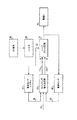
本発明の上記方法に従って作動できる電流コントローラを、図2の概略図に示す。明らかなように、該電流コントローラは、電磁石10に電流を供給する。電磁石10は、例えば、共振しやすい可動機械を支持する浮き台を浮揚させて、周囲の構造から共振を絶つために使用される電磁石からなるアレイのうちの一つであってもよい。
A current controller that can operate according to the above method of the present invention is shown in the schematic diagram of FIG. As is apparent, the current controller supplies current to the
この実施の形態においては、上記電流コントローラは、電圧要求信号12に応答して、電磁石10に電流を供給する。電圧要求信号12は、電磁石10によって生成すべき所望の力に従って生成される。例えば、電圧要求信号12は、上記可動機械を支持する上記浮き台の振動に関する情報を、連続する期間に、多数のモーションセンサから集めるグローバルコントローラ(図示せず)によって生成することができる。そして、該グローバルコントローラは、各連続する期間中に共振を低減するために、各電磁石10によって生成しなければならない力を決定する。該力が一旦、決まると、該グローバルコントローラは、各連続する期間に電磁石10に印加すべき必要な電圧を計算し、所望の力を実現して、これを上記電流コントローラに電圧要求信号12として供給する。別法として、該グローバルコントローラは、所望の力を示す信号を該電流コントローラへ供給し、該電流コントローラは、対応する電圧要求信号12を局所的に計算する。
In this embodiment, the current controller supplies current to the
電磁石10に供給された電流は、図1に示したものに相当するハーフブリッジ回路14の形態のスイッチング回路によって調整される。ハーフブリッジ回路14は、その対向するアームが、一対のダイオード16と一対のトランジスタ20a、20bとを有するブリッジを備える。ハーフブリッジ回路14への供給入力は、後に詳述するフィルタリングしたDC電源22として得られる+VsのDC電圧で供給される。電磁石10は、ハーフブリッジ回路14の出力の両端に接続されている。
The current supplied to the
スイッチング信号24a、24bは、箇所A、Bにおいてそれぞれトランジスタ20a、20bに印加される。該トランジスタは、MOSFET型のものでもよいが、他の一般に使用可能なタイプも同様に使用可能である。トランジスタ20a、20bは、電力損失が大きいそれらのコンダクタンスの線型領域を用いるのではなく、オン状態とオフ状態の間で、例えば、最少電流の状態と最大電流の状態との間で作動される。スイッチング信号24a、24bは、それぞれ、トランジスタ20a、20bを制御して、ハーフブリッジ回路14を、3つのモードのうちの1つで作動させる。
第1のモードにおいては、両トランジスタ20a、20bは、「オン」に切り替えられ、例えば、導通状態に切り替えられ、その結果、電磁石10は、+Vsの電圧を示し、
電流が、電磁石10を通って順方向にトランジスタ20aからトランジスタ20bへ、つまり、右から左へ流れる。
In the first mode, both
Current flows forward through the
第2のモードにおいては、トランジスタ20a、20bの一方が「オン」に切り替えられ、他方が「オフ」、つまり、非導通状態に切り替えられる。容易に分かるように、このモードにおいて、電磁石10は、0Vの電圧を示し、電流は、ハーフブリッジ回路14の一方のループを通ってのみ流れることが可能である。トランジスタ20aがオンに切り替えられ、かつトランジスタ20bがオフに切り替えられると、電流は、図1に示すハーフブリッジ14の上方のループに流れる。逆に、トランジスタ20bがオンに切り替えられ、かつトランジスタ20aが切り替えられると、電流は、図1に示すハーフブリッジ14の下方のループに流れる。しかし、トランジスタ20a、20bのどちらがオンしどちらがオフしているかに関係なく、電流は常に電磁石10を通って右から左へ流れ、この電流は、該電流経路における抵抗損失に従って大きさが低下する。
In the second mode, one of the
最後に、第3のモードにおいは、両トランジスタ20a、20bがオフになる。リザーバキャパシタ26は、フィルタリングされたDC電源22の両端に接続され、電磁石10の大きなインダクタンスは、電流が、電磁石10を通って、両ダイオード16を通る逆の経路に沿って流れることを保証する。この結果、電磁石10は、−Vsの電圧を示し、再び電流は、電磁石10を通って右から左へ流れる。この電流は、リザーバキャパシタ26が抵抗性損失によって放電するため、その大きさは減少する。
Finally, in the third mode, both
上記の構成は、電磁石10を通る単一方向の電流をもたらすことを認識されたい。また、この電流は、適切なスイッチング信号24a、24bをそれぞれトランジスタ20a、20bに供給して、電磁石10の両端に+Vs、0Vまたは−Vsの電圧を設定することによって制御することができることは明白である。
It will be appreciated that the above configuration provides a unidirectional current through the
各連続する期間のスイッチング信号24a、24bは、電圧要求信号12に応答して作動可能なスイッチング信号生成器システム28によって生成される。いずれか1つの期間中に電磁石10を通って流れる平均電流は、デューティサイクルを、該期間中に、電圧レベル+Vs、0Vまたは−Vsの各々で交番することによって変化させてもよい。電流の最大の増加は、期間を通して設定されている+Vsの電圧に対応し、電流の最大の減少は、期間を通して設定されている−Vsの電圧に対応する。
Each successive period of switching
電圧要求信号12に応答してスイッチング信号24a、24bを生成するのに加えて、スイッチング信号生成器システム28は、適切なスイッチング信号24a、24bが生成されたときに、2つの別の信号を考慮してもよい。これらの信号は、電圧センサ信号30および電流センサ信号32である。電圧センサ信号30は、ハーフブリッジ回路14の入力に与えられたフィルタリングされたDC電源22の電圧変動の予測手段である。電圧センサ信号30は、以下に詳細に説明するように、フィルタ38を通過した後に、DC電源36によって供給された電圧の変動を測定する電圧センサシステム34によって生成される。次に電流センサ信号32について説明すると、この信号32は、以下に詳細に説明するように、電磁石10を通って流れる、ハーフブリッジ回路14によって生成された電流を測定する電流センサ40によって生成される。本質的に、電流センサ信号32は、スイッチング信号生成器システム28により、トランジスタ20a、20bの電圧降下、およびそのキャパシタンスにより電磁石10によって示される電圧パルスの遅い立ち上がりおよび立ち下がり時間を計算するために使用される。
In addition to generating
スイッチング信号生成器システム28が、電圧センサ信号30または電流センサ信号32に関してスイッチング信号24a、24bを生成することは本質的ではないが、その場合、以下に明らかになるように、優れたノイズ制御を実現することができる。
It is not essential for the switching
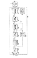
次に、スイッチング信号生成器システム28の構成要素について、詳細に説明する。図3aから最も明白に分かるように、電圧要求信号12、電圧センサ信号30および電圧センサ信号32は、電圧パルス幅生成器42に流れる。電圧パルス幅生成器42は、上記期間に対して電圧要求信号12を合わせるために、該期間に対して必要な電圧パルス幅44を計算し、電圧センサ信号30を参照して、フィルタリングされたDC電源22における電圧変動の予測値を、および電流センサ信号32を参照して、ハーフブリッジ回路14における電圧降下を補償する。例えば、電圧要求信号12が、該期間に対して1/2Vsの電圧を要求する場合、電圧パルス幅生成器42は、該期間の半分を占める+Vsのパルスを生成することになり、該期間の残りの半分は、0Vに設定される。
Next, the components of the switching
そして、計算された電圧パルス幅44は、ノイズシェーパ46に流れ、そこで、より高い周波数におけるノイズの増加を犠牲にして、当該周波数においてノイズが抑制されるように、該信号の量子化ノイズがシェーピングされる。ノイズシェーパ46を図3bにより詳細に示し、以下、より詳細に説明する。
The calculated
ノイズシェーピング後、その結果として生じた電圧パルス幅48は、トランジスタ20a、20bに流れるスイッチング信号24a、24bのそれぞれに対するパルス幅を計算するスイッチング信号パルス幅生成器50に流れる。これらのスイッチング信号パルス幅52は、ノイズシェーパ46を流れるノイズシェーピングされた電圧パルス幅48に対応するように設定される。スイッチング信号パルス幅52は、トランジスタ20a、20bのスイッチングに追従する電磁石10の両端の電圧の遅い立ち上がりおよび立ち下がり時間を補償するために、(電圧パルス幅生成器42およびノイズシェーパ46を通って届いた)電流センサ信号32に関して計算される。また、スイッチング信号パルス幅52は、補償された電圧パルス幅53を与えるように結合される。
After noise shaping, the resulting
スイッチング信号のパルス幅52は分かっているので、該信号は、必要な幅量子化構成のビット分解内で最も近い使用可能な量子化レベルに整合させるパルス幅量子化器54に流れる。量子化されたスイッチング信号パルス幅56は、対応する量子化された電圧パルス幅57を計算するのに使用され、該電圧パルス幅は、量子化の範囲内で補償された電圧パルス幅53とは異なる。スイッチング信号パルス幅52と量子化されたスイッチング信号パルス幅56の差、および補償された電圧パルス幅53と量子化された電圧パルス幅57の違いは、当然、量子化誤差であり、それらは、それ自体を量子化ノイズとして表わす。量子化された電圧パルス幅57は、量子化ノイズを低減するために、フィードバックループ58を介してノイズシェーパ46へ戻される。
Since the
次いで、量子化されたスイッチング信号パルス幅56は、スイッチング信号24a、24bに対する適切なエッジ位置を計算するスイッチング信号エッジ位置生成器60に流れる。計算されたスイッチング信号エッジ位置62は、精密なタイミングクロック66を参照して、スイッチング信号生成器64により実際のスイッチング信号24a、24bに変換され、それにより精度および同期を保証する。そして、スイッチング信号24a、24bは、それぞれ、トランジスタ20a、20bの図1の箇所AおよびBに流れる。トランジスタ20a、20bの作動は、電磁石10の両端の電圧を、+Vs、0Vおよび−Vsの値の間で変化させ、それにより、量子化された電圧パルス幅57に整合する量子化された電圧パルスを形成する。
The quantized switching signal pulse width 56 then flows to a switching signal
図3aのノイズシェーパ46を、図3bにより詳細に示す。図を見て分かるように、電圧パルス幅44は合流点68に流れ、そこで、ノイズシェーピングされた量子化誤差70が減ぜられる。実際には、2次ノイズシェーピング構成が用いられ、最後の1つの期間からのノイズシェーピングされた量子化誤差の重み付けされた分が、減ぜられる前の以前の期間からのノイズシェーピングされた量子化誤差70と結合される。このことは、以前の期間の量子化誤差により付加または損なわれた追加的な電圧の補償を含む、ノイズシェーピングされた電圧パルス幅48を生成する。そして、ノイズシェーピングされた電圧パルス幅48は、量子化された電圧パルス幅57が、上述したようにそれから導出される量子化されたスイッチング信号パルス幅56を生成するのにも用いられるスイッチング信号パルス幅52を生成するのに用いられる。
The noise shaper 46 of FIG. 3a is shown in more detail in FIG. 3b. As can be seen, the
量子化された電圧パルス幅57は、フィードバックループ58に沿って流れ、量子化誤差74を与える合流部72において、補償された電圧パルス幅53から減ぜられる。それに続いて、量子化誤差74は、従来よく知られているように、2次ノイズシェーピングを用いて、当該周波数帯の全域で量子化ノイズを抑制するノイズシェーピングフィルタ76によって処理される。
The quantized
次に、ノイズシェーピングフィルタ76によって生成された処理された量子化誤差78は、該処理された量子化誤差が、連続する期間に、電圧パルス幅44から減ぜられることを保証するために、符号80において一期間遅延を通過する。よってネガティブフィードバックが完成する。
Next, the processed quantization error 78 generated by the
次いで、電圧センサシステム34について、特に図4を参照してより詳細に説明する。上述したように、ハーフブリッジ回路14への電源入力は、フィルタリングされたDC電源22によって供給される。これは、DC電源36からの信号に含まれる可能性がある電源線リプルをできるだけ取り除くために、フィルタ38を通過するDC電源36から得られる。
The
また、リザーバキャパシタ26は、電磁石10を通って流れる電流の変化に応答して充放電するので、ハーフブリッジ回路14のリザーバキャパシタ26の両端の電位の変化により、フィルタリングされたDC電源22の相互変調がある場合がある。相互変調は、それ自体、電磁石10によって示される量子化された電圧パルスにおける振幅変調として現れる。明らかに、所望の+Vs、0Vおよび−Vsのパルスレベルからのずれは、満たされない電圧要求信号12をもたらし、上記磁石を流れる電流は、(例えば、上記可動機械の振動を絶つために)意図した磁界を生成するのに必要な電流からドリフトする。
In addition, since the reservoir capacitor 26 is charged and discharged in response to a change in the current flowing through the
フィルタリングされたDC電源22の不必要な変動を補償するために、予測する電圧センサシステム34が用いられる。フィルタリングされたDC電源22の変動のフィードスルーを指示する信号処理遅延手段は、スイッチング信号生成器28に遅く到達して、有効な補償を実現できる。すなわち、フィードフォワード予測電圧センサシステム34が用いられる。電圧センサ82は、図4に示すように、フィルタリングされたDC電源22を測定する。これらの測定値の逆数が7タップ有限インパルス応答(finite impulse response;FIR)フィルタ86による使用のために符号84において計算される。これらの要素は、当業者が容易に認識できるように、容易に使用可能である。FIRフィルタ86は、次の期間にわたる1/Vsの適当な値を予測するのに使用され、この値を、予想される電圧の増加または減少にそれぞれ比例して、電圧パルス幅44に重み付けを付加または減じることができるように、電圧センサ信号30としてスイッチング信号生成器28へ送る。
A predictive
電磁石10の制御品質は、電磁石10によって示される電圧のために考慮された有限で重要な時間に影響を受けて、トランジスタ20a、20bのうちの一方のスイッチングオフ時に低下する(以下に説明するように他の要因もある)。該電圧の線形性の減少は、電磁石10に内在する静電容量を放電できるように速く低下できるため引き起こされる。電流は、図2に示す電流センサ40によって測定され、その結果生じる電流センサ信号32は、スイッチング信号パルス幅52を計算して、以前の期間に測定された電流に対応して、電圧の遅い減少を補償するように、スイッチング信号生成器28へ流れる。
The control quality of the
上記電流コントローラの構成要素について説明してきたので、次に、電磁石10によって示される電圧におけるパルスの幅、およびスイッチング信号24a、24bのパルスの幅が、どのようにして決定されるかに注意して、上記電流コントローラの動作方法について説明する。
Having described the components of the current controller, it will now be noted how the pulse width at the voltage indicated by the
各期間は、電圧要求12に見合うように該期間に、電磁石10の両端に平均電圧を生じる要求されたスイッチング信号24a、24bも計算するスイッチング信号生成器28によって受けられる電圧要求12によって始まる。そしてスイッチング信号生成器28は、正確なタイミングクロック66を参照して、該期間に正確に同期させて、スイッチング信号24a、24bをそれぞれトランジスタ20a、20bへ送る。
Each period begins with a
図3aを見て最もよく分かるように、電圧要求12は、電圧パルス幅生成器42によって受けられる。上述したように、電圧パルス幅44は、0Vのベースラインに対して+Vsまたは−Vsのどちらかの単一のパルスが使用されると仮定すると、数秒で生成される。電圧パルス幅44は、(1/Vs)estと表わすことができる電圧センサ信号30として供給される上記期間のVsの予測測定値に従って、フィルタリングされたDC電源22の変動に関して生成される。
As best seen in FIG. 3 a, the
さらに、ダイオード16(Vdiode)およびトランジスタ20a、20bのフォワード電圧降下も考慮される。これらの影響が考慮されない場合には、出力電圧オフセットおよび出力電圧振幅の変化が見られることになる。トランジスタ20a、20bの両端の電圧降下は、典型的な動作条件の間にかなり変化することが知られている。該電圧降下の大きさを予測するために、典型的な動作点に対する対応するデバイスデータシートから、トランジスタ20a、20bのドレイン・ソース抵抗(RDS)の値が取得される。この抵抗は、トランジスタ20a、20bのフォワード電圧降下を予測するために、(電磁石10を流れる電流Imagを与える)電流センサ信号32と共に用いられる。Vdiodeの値は、上記電流コントローラ動作条件にわたって一定であると仮定されるため、上記対応するデバイスデータシートから、典型的な動作点を表わす値を選択することによって得られる。
Furthermore, the forward voltage drop of the diode 16 (Vdiode) and the
そして、上記出力電圧の微妙な調節のために、小さなDCオフセット電圧補正(Voffset)が用いられる。この値は、較正によって得られる。 A small DC offset voltage correction (Voffset) is used for fine adjustment of the output voltage. This value is obtained by calibration.
要求された電圧12(Vdemand)は、損失を補償するために、ダイオード16およびトランジスタ20a、20bの電圧降下の付加によって調整される(オフセットに対する正および負のサインの使用が、正しい補償を保証する)。すなわち、要求された電圧パルス幅44(Wreq)は、
から計算することができる。ただし、Wfullは、数秒間の最大パルス幅である。この実施例においては、64kHzのパルス繰り返し周波数を用い、タイミングクロックの周波数は、15.625の周期幅を示す32.768MHzであった。当然、他のパルス繰り返し周波数も、ノイズ要求、およびより高い周波数に対処する構成要素の損失または有効性により、代わりになることが可能である。 Can be calculated from However, Wfull is the maximum pulse width for several seconds. In this example, a pulse repetition frequency of 64 kHz was used, and the frequency of the timing clock was 32.768 MHz indicating a period width of 15.625. Of course, other pulse repetition frequencies can be substituted due to noise requirements and the loss or effectiveness of components that deal with higher frequencies.
式(1)から電圧パルス幅44が、要求された電圧の極性を反映するサインを有し、例えば、該サインは、0V〜+Vsの電圧要求12の場合には正であり、0V〜−Vsの電圧要求12の場合には負であることに注意されたい。このサインは、後の計算の全体に媒介される。さらに、電圧パルス幅44は、0Vベースラインから離れた時間の測定値であり、すなわち+Vsにおけるパルスおよび−Vsにおけるパルスの幅である。
From equation (1), the
式(1)は、高いレベルの精度をもたらすが、ブラケットの最初のセットに含まれる (Vdemand以外の)全てのまたはどの項も含まれる必要はなく、この場合、電磁石10の性能の低下を許容することができる。
Equation (1) provides a high level of accuracy, but does not need to include all or any terms (other than Vdemand) that are included in the first set of brackets, in which case the performance degradation of the
電圧パルス幅44は、ノイズシェーパシステム46へ送られて、ノイズシェープした電圧パルス幅48(Wsh)を生成する。これは、上述したように、以前の期間のパルス (WQE-1)の幅における量子化誤差を参照して、および、最後の1つの期間のパルス(WQE-2)も参照して計算される。ノイズシェーピングされた電圧パルス幅48は、
で表わされる。ただし、fPRF は、パルス繰り返し周波数(上述したように、64kHz)であり、またfnotchは、上記シェーピングされたノイズのノイズスペクトルにおける必然的なノッチに対して選択された周波数である。本実施形態においては、これは1kHzになるように選択された。 It is represented by However, f PRF is a pulse repetition frequency (64 kHz as described above), and fnotch is a frequency selected for an inevitable notch in the noise spectrum of the shaped noise. In this embodiment, this was selected to be 1 kHz.
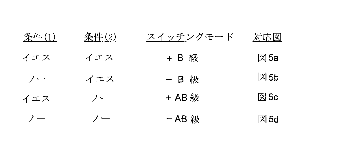
そして、ノイズシェーピングされた電圧パルス幅48は、スイッチング信号24a、24bのパルスに対して対応する幅を生成するスイッチング信号パルス幅生成器50へ送られる。しかし、トランジスタ20a、20bをスイッチングする4つのモードがあり、正しいモードを実施しなければならない。従って、次に、それらの4つのモードを、図5a〜dを参照して詳細に説明する。この点に関して上述したことを要約すると、トランジスタ20a、20bが次のようにスイッチングされた場合、次のような電圧が、電磁石10によって示される。
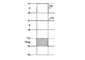
図5aは、スイッチングシーケンスを示し、電圧要求12は、正の電圧、例えば、0〜+Vsのためのものである。トランジスタ20a、20bの各スイッチング動作に内在する電力損失を避けるために、デフォルトのスイッチングモードは、一方のトランジスタ20aのみが期間中にスイッチングされ、他方のトランジスタ20bは、該期間中は、そのオン状態のままである、いわゆる「B級」モードである。このようにして、トランジスタ20bにおいては、スイッチングにより電力は損なわれない。また、多くの用途において、電圧要求12は、多くの連続する期間に正または負のままになりやすいため、一方のトランジスタ20a、20bを、その期間中に不変の状態にしておくことができ、それにより、そのトランジスタ20a、20bのスイッチングに内在するいかなる電力損失も避けられる。図を見て分かるように、スイッチング信号24aの単一のパルスは、該期間内の中心で生成されて、電磁石10の両端に電圧を生成して、単一の対応する+Vsのパルス(図5aのハッチングした部分)が、0Vのベースラインから立ち上がって、要求された正の電圧を生じている。
FIG. 5a shows the switching sequence, where the
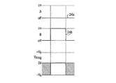
図5bは、負の電圧、つまり、0〜−Vsに対する電圧要求に対応する第2のモードの動作を示す。ここでも、トランジスタ20a、20bのB級スイッチングが用いられ、このとき、トランジスタ20aは、その期間中オフ状態のままであり、トランジスタ20bは該期間内に中心パルスを有するそのスイッチング信号24bによってスイッチングされている。電磁石10によって示された、結果として生じる電圧は、該期間の始めと終わりにおいて0Vベースラインから伸びる一対の−Vsのパルスを有する。すなわち、図5bでハッチングした2つのパルスは、要求された負の電圧パルスを形成するように結合する。そのため、−Vsのパルスを生じるスイッチング信号20bの中心パルスではなく、むしろ周辺の領域である。従って、それは、電磁石10によって示される電圧の−Vsのパルスの幅に相当するスイッチング信号24bの中心パルスの幅より小さい該期間の全幅である。上述したように、連続する負の電圧が要求された場合、トランジスタ(この場合20a)を不変状態にしておくことができることを認識されたい。
FIG. 5b shows the second mode of operation corresponding to a negative voltage, ie a voltage requirement for 0 to −Vs. Again, class B switching of the
厳密に言えば、ゼロ電圧が要求されたときに生じる別のモードについて、完全性のために言及すべきである。これは、上記期間中ずっと、トランジスタ20aをオフにし、かつトランジスタ20bをオンにすることによって実施することができる。
Strictly speaking, another mode that occurs when zero voltage is required should be mentioned for completeness. This can be done by turning off
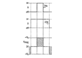
B級スイッチングは、両トランジスタ20aおよび20bを一つの期間内にスイッチングしなければならない場合の電力損失の低減により好適であり、小さな正の電圧または小さな負の電圧が要求された場合に、相反する要求が生じる。小さな正の電圧の場合、このことは、電磁石10によって示される電圧を、急速に+Vsに昇圧した後、0Vに下げなければならないため、該電磁石10によって示される電圧において狭小なパルスをもたらす。小さな負の電圧の場合には、問題は、連続する期間の始めと終わりにおいて、電圧を急速に、−Vsに降圧した後、0Vまで上げなければならないということにある。トランジスタ20a、20bの遅い応答および立ち上がりは、パルスの波形縁部に歪みを付加し、電圧制御の不足につながる。これらの影響は、特有の小さなパルスに対して問題になり、立ち上がり波形間の安定した平坦領域が失われる。このことは、上記電流コントローラの線形性の喪失につながる。この問題を克服するために、しきい値パルス幅Wthreshが設定され、電圧要求12を満たすために、該しきい値未満のパルス幅が要求された場合、一つの期間において両トランジスタ20a、20bがスイッチングされるいわゆる「AB級」に変更される。
Class B switching is more suitable for reducing power loss when both
図5cは、小さな正の電圧要求12に対するAB級スイッチングの事例を示す。B級スイッチングを用いて実施した場合、上記しきい値幅未満の電磁石10によって示される電圧の単一のパルスが生じる。これを避けるために、トランジスタ20bを、期間中ずっとオン状態にして、該トランジスタがスイッチングされて、該期間のほとんどを占める中心オンパルスを生成するのではなく、トランジスタ20aがスイッチングされて、上記しきい値幅に要求された幅を加えたものに等しい幅を有する中心オンパルスが生成される。電磁石10によって示される結果として生じる電位は、小さな下方に伸びるパルスによって−Vsで始まりかつ終わり、この場合両トランジスタ20a、20bはオフであり(実線のハッチング領域で示す)、これは、トランジスタ20bがオンであり、かつトランジスタ20aがオフである0Vにおける領域に進み、これらの領域は、+Vsにおける中心パルスで合わさり、この場合、両トランジスタ20a、20bはオンである(破線のハッチング領域で示す)。該ハッチングした領域の幅は、簡単のため誇張されており、また、実際のしきい値幅を測定するのに用いるべきではない。上記期間中の電磁石10によって示される平均電位は、上記実線でハッチングされた領域よりも小さい上記破線でハッチングされた領域に相当し、これは明らかに、最終的な小さな正の電圧をもたらす。
FIG. 5 c shows the case of class AB switching for a small
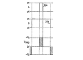
同様に、図5dは、B級スイッチングを用いるべき場合に、連続する期間に、上記しきい値幅以下である−Vsの幅をもたらすであろう小さな負の電圧要求12に応答するAB級スイッチングの事例を示す。最少−Vsのパルス幅を維持するために、トランジスタ20bは、期間中のほとんどにわたって中心に伸びるオンパルスを有するようにスイッチングされる。トランジスタ20aは、B級スイッチングの時のようにオフ状態のままにされるのではなく、中心オンパルスを有するようにスイッチングされる。電磁石10によって示される結果として生じる電位は、−Vsに対応する上記実線でハッチングされた領域が、+Vsに対応する上記破線でハッチングされた領域よりも大きくなるように結合し、すなわち、小さな負の平均電位を示す電磁石10をもたらすことを除いて、図5cを参照して説明したものに対応する形状を有する。
Similarly, FIG. 5d shows that when class B switching is to be used, class AB switching in response to a small
従って、スイッチングモードのタイプは、次の条件(1)、(2)をテストすることによって決まる。
ただし、Wcapは、電磁石10の静電容量(Cmag)を補償するように計算された幅調節値である。この静電容量は、上述したように、電磁石10によって示される電圧レベル間に遅い立ち上がり時間および立ち下がり時間を引き起こし、そのため、パルスを人為的に長くするという影響を有する。すなわち、制御は失われる。上記幅調節値は、次式から計算される。
ただし、電磁石10を流れる電流の最大値(Imag)または最少電流値(Imin)が用いられる。該最少電流値は、ゼロで分割されること、および、小さな電流のみが、電磁石10を流れる場合に生じる問題を避けるために、この計算で用いる電流の下限に相当する。
However, the maximum value (Imag) or the minimum current value (Imin) of the current flowing through the
条件(1)および(2)をテストすることの結果に適するスイッチングの種類を以下に示す。
そして、スイッチング信号パルス幅52は、次のように、適切なスイッチングモードに対して計算される。以下の等式において、WA およびWB は、それぞれ、スイッチング信号24aおよび24bのパルスの幅である。WEAおよびWEBは、それぞれスイッチング信号24aおよび24bに応答して生成されたパルスの実際の幅における最終的な実効誤差である(これらの値は、較正によって決定される)。Wminは、AB級モードの時に付加される固定されたオフセットである。
The switching
+B級
つまり、トランジスタ20aは、ノイズシェーピングされた電圧パルス幅48から静電容量の補償および最終的な実効誤差を減じたパルスを有し、トランジスタ20bは、期間中ずっとオンのままである。
That is,
−B級
つまり、トランジスタ20aは、期間中ずっとオフのままであり、トランジスタ20bは、ノイズシェーピングされた電圧パルス幅48を減じ(ノイズシェーピングした電圧パルス幅48が、−Vsにおける電圧パルス幅を反映するのに対して、我々は、0Vにおける中心領域を生成するスイッチング信号のパルスに対する幅を設定することを思い起こす)、かつ静電容量の補償および最終的な実効誤差を減じた全期間幅に等しい中心パルスを有する。
That is,
+AB級
つまり、トランジスタ20aは、上記しきい値幅が越えられることを保障する固定されたオフセットを加え、静電容量の補償および最終的な実効誤差を減じた、ノイズシェーピングされた電圧パルス幅48のパルスを有し、トランジスタ20bは、最終的な利得が、電磁石10の両端の出力電圧に生じないことを保証する固定されたオフセットを除き、かつ静電容量の補償および最終的な実効誤差を除いて、期間中ずっとオンのままである。
That is, the
−AB級
つまり、−B級スイッチングの場合と同様であるが、ここで、トランジスタ20aは、静電容量の補償および最終的な実効誤差を減じた固定されたオフセット幅を有するパルスを含み、トランジスタ20bは、期間の間の電圧変化の間の最少間隔を保障する固定されたオフセットに対応して、その中心パルスに幅の低減を有する。
That is, similar to the case of -B switching, where
スイッチング信号パルス幅52を計算してきたが、これらの幅52は、数秒毎であり、また0から該期間の全幅までの範囲のいずれかの値をとることができる(上記パルス繰り返し周波数の逆数、例えば、15.625μs)。しかし、最終的なスイッチング信号は変調されたパルス幅であるため、スイッチング信号パルス幅52は、一つの期間内で使用可能な周期カウントの数に適合するように量子化されるように、正確なタイミングクロック66の周期カウントに変換しなければならない(パルス繰り返し周波数と正確なタイミングクロック66の周波数fclockとの組合せが、期間毎に512周期カウントを生じることを言及してきた)。この機能は、スイッチング信号パルス幅量子化器54によって実行される。
Although the switching
スイッチング信号パルス幅量子化器54は、以下の単純な式から、周期カウントの数 (トランジスタ20aおよび20bに対して、それぞれNA およびNB )を計算して、それらの値を量子化されたスイッチング信号パルス幅56として送る。
また、NA およびNB は、次式に従って、量子化誤差74(WQE)を計算するのにも用いられる。
そしてWQEは、上述したように、次の期間において、WQE-1およびWQE-2として用いられる。 And W QE, as described above, in the next period, used as W QE-1 and W QE-2.
正確なタイミングクロック66の周期カウントのユニットにおいて、量子化されたスイッチング信号パルス幅56が分かっている場合、スイッチング信号エッジ位置生成器60は、該正確な周期カウントを生成し、スイッチング信号24a、24bのエッジが発生する。
If the quantized switching signal pulse width 56 is known in the accurate timing clock 66 period counting unit, the switching signal
上記パルスは、信号歪みを最少化するために、交番奇数非対称を用いて配置される。この歪みは、奇数番の周期カウントのパルスが必要な場合に生じる。このようなパルスは、期間内の中心に配置することができず、エッジが、周期カウントの始めと終わりに一致しなければならないという制約を与える。該パルスが、常に半周期早くまたは半周期遅くなるように配置されている場合には、歪みが結果として生じる。この歪みは、交番奇数非対称を用いることにより、例えば、立ち上がりエッジと立ち下がりエッジとの間のオフセットを該期間の半分で交番することによって最少化される。アルゴリズムを適用すると、トランジスタ20aに対するオンエッジ位置およびオフエッジ位置は、次のように与えられる。
The pulses are arranged using alternating odd asymmetry to minimize signal distortion. This distortion occurs when an odd number of period count pulses are required. Such a pulse cannot be centered in the period, giving the constraint that the edge must coincide at the beginning and end of the period count. If the pulses are always arranged to be half a cycle early or half a cycle late, distortion will result. This distortion is minimized by using alternating odd asymmetry, for example by alternating the offset between the rising and falling edges in half of the period. When the algorithm is applied, the on-edge position and the off-edge position for the
NA が偶数の場合、ONA =1/2(Nfull−NA )
その他の場合、ONA =1/2(Nfull−NA +dA )およびdA =−dA
また、OFFA =ONA +NA
ただし、Nfullは、周期カウント(512)の最大数であり、dA は、最初、+1に設定され、その値は、一つの期間から次の期間へ伝えられる。認識されるように、トランジスタ20bに対するエッジ位置は、対応する方法で(例えば、下付き文字「A」と下付き文字「B」と交換することによって)決定する。
When N A is an even number, ON A = 1/2 (Nfull-N A )
In other cases, ON A = 1/2 (Nfull-N A + d A ) and d A = -d A
In addition, OFF A = ON A + N A
However, Nfull is the maximum number of period counts (512), d A is initially set to +1, and the value is transmitted from one period to the next. As will be appreciated, the edge position for
スイッチング信号24a、24bのパルスのエッジ位置が分かっている場合、それらの値は、スイッチング信号エッジ位置62としてスイッチング信号生成器64へ送られる。そしてスイッチング信号生成器64は、スイッチング信号エッジ位置62を正確なタイミングクロック66の周期カウントに同期させて、その後、それぞれトランジスタ20a、20bへ送られる実際のスイッチング信号24a、24bを生成する。
If the edge positions of the pulses of the switching signals 24 a, 24 b are known, those values are sent to the switching signal generator 64 as the switching
すなわち、ハーフブリッジ回路14は、電圧要求12に対応して、電磁石10の両端に平均電圧を生成するように作動する。
That is, the
当業者は、本発明の範囲を逸脱することなく、本願明細書に記載した上記実施の形態に対して変更例を実施することができることを認識するであろう。 Those skilled in the art will recognize that modifications can be made to the above-described embodiments described herein without departing from the scope of the present invention.
例えば、上記の実施の形態は、グローバルコントローラにより、所望の値に従って生成することができる電圧要求信号12に応答して、電磁石10に電流を供給する電流コントローラについて記載している。しかし、該電流コントローラは、電圧要求信号12ではなく、電流要求信号88に応答して作動してもよい。この信号は、第1の実施の形態の電圧要求信号12の生成に関して説明したような方法と同じ方法で、該グローバルコントローラによって生成することができる。
For example, the above embodiments describe a current controller that supplies current to the
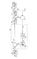
このような構成を図6に示す。この図は、図2と同様であるが、電流要求モードで作動するのに必要な追加的な構成要素を示している。図2からの全ての構成要素(および図3および4に詳細に示す構成要素)は、上記電流コントローラに含まれており、該電流要求モードのこの議論に関連する構成要素のみを、明確化のために図6に示す。図から明らかなように、主な変化は、符号87で示す制御ループを含んでいることである。
Such a configuration is shown in FIG. This figure is similar to FIG. 2, but shows the additional components necessary to operate in the current demand mode. All components from FIG. 2 (and the components shown in detail in FIGS. 3 and 4) are included in the current controller, and only the components relevant to this discussion of the current demand mode are clarified. This is shown in FIG. As is apparent from the figure, the main change is that a control loop denoted by
動作の一つのモードにおいては、電流要求信号88(明確化のために符号88aで示す)は、比較器90において、電流センサ信号32と比較される。電流センサ信号32は、電流センサ40の出力から得られ、電磁石10の流れる電流の測定を示す。電流センサ信号32を電流要求信号88aと比較することによって、電磁石10を流れる電流の要求された電流からのずれを示すエラー信号92が生成される。エラー信号92は、制御ループ利得と、制御ループフィルタと、電流/電圧転送モデルとを含んで、電圧要求信号12aを生成するフィルタ94に送られる。電圧要求信号12aは、3方スイッチ96を介してスイッチング信号生成器システム28へ送られる。
In one mode of operation, the current request signal 88 (denoted 88a for clarity) is compared with the
上記電流電圧転送モデルの不正確さは、電流センサ40を用いて制御ループ87によって補正される。上記電流コントローラの性能は、該電流電圧転送モデルの正確さよりも、電流センサ40のノイズ性能および精度により依存する。必要に応じて、例えば、最良のダイナミックレンジを与えるために、電流センサの組合せを用いてもよい。
The inaccuracy of the current voltage transfer model is corrected by the
(電流センサ信号32を介した)電磁石電流のドリフトを補正する制御ループ87が必要ない動作の代替のモードにおいては、図6に示すように、電流要求信号88を、符号88bで直接、電圧要求生成器100へ送ることができる。電圧要求生成器100は、電圧要求生成器100が、要求された電流要求88を生成するのに必要な適切な電圧要求を予測できるように、電磁石負荷特性のモデルを含むフィルタを用いて、電圧要求信号12bを生成する。電圧要求信号12bは、3方スイッチ96を介してスイッチング信号生成器システム28へ送られる。当然、電磁石10へ送られた結果の電流の精度は、電圧要求信号12bを生成する負荷モデルの精度に強く依存する。
In an alternative mode of operation that does not require a
必要に応じて、上記電流コントローラは、電圧要求モードまたは電流要求モードのいずれかで作動するように適応させることができる。例えば、3方スイッチ96は、スイッチング信号生成器システム28へ送られる電圧要求信号12を生成するために、フィルタ94によって生成された電圧要求入力12a、または、電圧要求生成器100によって生成された電圧要求入力12b、あるいは、直接電圧要求入力12c(例えば、グローバルコントローラまたは同等物から電圧要求を直接送るライン)の間で切り替えるために使用することができる。
If desired, the current controller can be adapted to operate in either voltage demand mode or current demand mode. For example, the three-way switch 96 may be the
Claims (35)
(a)一つの期間において、上記出力に供給すべき電気信号の所望の電圧を示す電圧要求信号を受ける工程と、
(b)上記電圧要求信号を参照するとともに、上記スイッチング回路の電圧オフセットを参照して、第1および第2のスイッチング信号を生成する工程と、
(c)上記第1および第2のスイッチング信号を、上記期間中にそれぞれ上記第1および第2のスイッチに印加する工程とを備え、
上記スイッチング信号は、上記スイッチを、オンおよびオフ状態の間でスイッチさせ、上記第1および第2のスイッチのオンおよびオフ状態の様々な組合せ間のスイッチングは、+Vs、0Vおよび−Vsのレベルでの電圧パルスによって、上記出力に電気信号を生成し、
上記第1および第2のスイッチング信号は、上記期間中に上記出力に供給される電気信号の平均電圧が、所望の電圧に実質的に等しいように生成されることを特徴とするスイッチング回路を作動させる方法。 A method of operating a switching circuit comprising an input receiving a DC signal of voltage + Vs, an output, and first and second switches,
(A) receiving a voltage request signal indicating a desired voltage of an electrical signal to be supplied to the output in one period;
(B) generating the first and second switching signals by referring to the voltage request signal and referring to the voltage offset of the switching circuit;
(C) applying the first and second switching signals to the first and second switches, respectively, during the period;
The switching signal causes the switch to switch between on and off states, and switching between various combinations of the on and off states of the first and second switches is at levels of + Vs, 0V and −Vs. An electric signal is generated at the output by the voltage pulse of
The first and second switching signals actuate a switching circuit, characterized in that an average voltage of an electrical signal supplied to the output during the period is substantially equal to a desired voltage. How to make.
Applications Claiming Priority (2)
| Application Number | Priority Date | Filing Date | Title |
|---|---|---|---|
| GBGB0200024.8A GB0200024D0 (en) | 2002-01-02 | 2002-01-02 | A switching circuit and a method of operation thereof |
| PCT/GB2002/005733 WO2003061103A2 (en) | 2002-01-02 | 2002-12-17 | A switching circuit and a method of operation thereof |
Publications (2)
| Publication Number | Publication Date |
|---|---|
| JP2005515744A true JP2005515744A (en) | 2005-05-26 |
| JP4068568B2 JP4068568B2 (en) | 2008-03-26 |
Family
ID=9928541
Family Applications (1)
| Application Number | Title | Priority Date | Filing Date |
|---|---|---|---|
| JP2003561076A Expired - Fee Related JP4068568B2 (en) | 2002-01-02 | 2002-12-17 | Switching circuit and operating method thereof |
Country Status (6)
| Country | Link |
|---|---|
| US (1) | US7692337B2 (en) |
| EP (1) | EP1461856A2 (en) |
| JP (1) | JP4068568B2 (en) |
| AU (1) | AU2002352417A1 (en) |
| GB (1) | GB0200024D0 (en) |
| WO (1) | WO2003061103A2 (en) |
Cited By (1)
| Publication number | Priority date | Publication date | Assignee | Title |
|---|---|---|---|---|
| JP2013162544A (en) * | 2012-02-01 | 2013-08-19 | Nippon Steel & Sumitomo Metal | Method of controlling power conversion system, and power conversion system |
Families Citing this family (1)
| Publication number | Priority date | Publication date | Assignee | Title |
|---|---|---|---|---|
| US9048831B2 (en) * | 2012-07-13 | 2015-06-02 | General Electric Company | Systems and methods for regulating semiconductor devices |
Family Cites Families (38)
| Publication number | Priority date | Publication date | Assignee | Title |
|---|---|---|---|---|
| GB2014388B (en) | 1977-10-28 | 1982-05-19 | Ferranti Ltd | Transistor bridge circuit |
| DE3037305C2 (en) | 1980-10-02 | 1986-04-03 | Flowtec AG, Reinach, Basel | Arrangement for generating constant magnetic fields of alternating polarity for magnetic-inductive flow measurement |
| US4585986A (en) | 1983-11-29 | 1986-04-29 | The United States Of America As Represented By The Department Of Energy | DC switching regulated power supply for driving an inductive load |
| DE3402759A1 (en) | 1984-01-27 | 1985-08-01 | Robert Bosch Gmbh, 7000 Stuttgart | CURRENT CONTROLLER FOR ELECTROMAGNETIC ACTUATORS |
| GB8530930D0 (en) | 1985-12-16 | 1986-01-29 | Mansfield P | Inductive circuit arrangements |
| DE3603071A1 (en) | 1986-02-01 | 1987-08-06 | Leybold Heraeus Gmbh & Co Kg | DC-AC CONVERTER WITH ASYMMETRIC SEMI-BRIDGE CIRCUIT |
| DE3638174A1 (en) | 1986-11-08 | 1988-05-19 | Parker Hannifin Nmf Gmbh | Driver circuit for inductive loads |
| JP2578134B2 (en) | 1987-10-22 | 1997-02-05 | 白木金属工業株式会社 | Drive circuit for solenoid |
| JPH01247507A (en) | 1988-03-30 | 1989-10-03 | Nippon Steel Corp | Method for converting molten metal into drops |
| US4890188A (en) | 1988-10-04 | 1989-12-26 | Lockwood Technical, Inc. | Solenoid driver system |
| JP2799886B2 (en) | 1989-09-11 | 1998-09-21 | 株式会社セコー技研 | Energization control device for inductance load |
| DE4018930C2 (en) | 1990-06-13 | 1994-07-14 | Klug Rolf Dieter Dr Ing | Bridge branch of DC choppers and pulse inverters with regulated cross current |
| CA2053540C (en) | 1991-10-11 | 2001-05-15 | Gyula Eisenbart | Inductive load switch utilizing simplified gating |
| JPH0683402A (en) * | 1992-08-31 | 1994-03-25 | Toshiba Corp | PWM drive circuit |
| JP3070355B2 (en) | 1993-10-06 | 2000-07-31 | トヨタ自動車株式会社 | Solenoid drive control device for automatic transmission |
| DE4413240A1 (en) | 1994-04-16 | 1995-10-19 | Bosch Gmbh Robert | Device and a method for controlling an electromagnetic consumer |
| US5559467A (en) * | 1995-01-27 | 1996-09-24 | The Regents Of The University Of California | Digital, pulse width modulation audio power amplifier with noise and ripple shaping |
| DE69523752T2 (en) | 1995-08-31 | 2002-08-29 | St Microelectronics Srl | Method and circuit for pulse width modulated control of a bridge and a plate drive and using the same |
| JP3108626B2 (en) | 1996-03-26 | 2000-11-13 | シャープ株式会社 | Inverter bridge gate drive signal generation method |
| US5977725A (en) | 1996-09-03 | 1999-11-02 | Hitachi, Ltd. | Resonance type power converter unit, lighting apparatus for illumination using the same and method for control of the converter unit and lighting apparatus |
| JP3758305B2 (en) | 1996-09-17 | 2006-03-22 | 株式会社日立製作所 | Lighting device |
| JP3801273B2 (en) | 1996-09-20 | 2006-07-26 | カヤバ工業株式会社 | Solenoid valve drive circuit |
| DE19808297A1 (en) | 1997-03-05 | 1998-09-10 | Mannesmann Rexroth Ag | Current controlled end stage for electromagnetic drives, esp. for proportional magnets used as valve drive |
| US5847554A (en) * | 1997-06-13 | 1998-12-08 | Linear Technology Corporation | Synchronous switching regulator which employs switch voltage-drop for current sensing |
| DE19728318C1 (en) | 1997-06-27 | 1999-04-01 | Daimler Benz Ag | Dynamic suppression of DC current in single-phase transformer |
| JPH1169629A (en) | 1997-08-21 | 1999-03-09 | Nissin Electric Co Ltd | Control method for active filter |
| DE19747033A1 (en) | 1997-10-24 | 1999-04-29 | Daimler Chrysler Ag | Electronic switching device for magnets, esp. electromagnetic valve control elements for an internal combustion engine |
| JP3744680B2 (en) | 1998-03-31 | 2006-02-15 | 富士通株式会社 | Power supply device and method for controlling power supply circuit |
| JP2000006523A (en) | 1998-06-24 | 2000-01-11 | Dainippon Printing Co Ltd | Thermal transfer sheet and IC card using the same |
| US6213442B1 (en) | 1998-10-08 | 2001-04-10 | Lord Corporation | Isolation system for isolation tables and the like |
| US6081104A (en) * | 1998-11-20 | 2000-06-27 | Applied Power Corporation | Method and apparatus for providing energy to a lighting system |
| FR2786920B1 (en) * | 1998-12-07 | 2001-01-12 | Schneider Electric Ind Sa | STANDARD CONTROL DEVICE OF AN ELECTROMAGNET FOR OPENING OR CLOSING A CIRCUIT BREAKER |
| WO2000074222A1 (en) | 1999-05-27 | 2000-12-07 | Hitachi, Ltd. | H-type bridge circuit and integrated circuit |
| EP1081842B1 (en) * | 1999-09-01 | 2004-05-26 | Ramachandran Ramarathnam | A multi-speed motor controller |
| DE50010766D1 (en) | 1999-09-16 | 2005-08-25 | Siemens Ag | METHOD FOR CONTROLLING AN ELECTROMECHANICAL ACTUATOR |
| US6577488B1 (en) | 2000-01-14 | 2003-06-10 | Motorola, Inc. | Inductive load driver utilizing energy recovery |
| DE10018175A1 (en) | 2000-04-12 | 2001-10-25 | Bayerische Motoren Werke Ag | Circuit arrangement for operating a highly dynamic electromagnetic lifting armature actuator |
| GB0200027D0 (en) * | 2002-01-02 | 2002-02-13 | Bae Systems Plc | Improvements relating to operation of a current controller |
-
2002
- 2002-01-02 GB GBGB0200024.8A patent/GB0200024D0/en not_active Ceased
- 2002-12-17 EP EP02788137A patent/EP1461856A2/en not_active Withdrawn
- 2002-12-17 WO PCT/GB2002/005733 patent/WO2003061103A2/en not_active Ceased
- 2002-12-17 US US10/500,623 patent/US7692337B2/en not_active Expired - Fee Related
- 2002-12-17 AU AU2002352417A patent/AU2002352417A1/en not_active Abandoned
- 2002-12-17 JP JP2003561076A patent/JP4068568B2/en not_active Expired - Fee Related
Cited By (1)
| Publication number | Priority date | Publication date | Assignee | Title |
|---|---|---|---|---|
| JP2013162544A (en) * | 2012-02-01 | 2013-08-19 | Nippon Steel & Sumitomo Metal | Method of controlling power conversion system, and power conversion system |
Also Published As
| Publication number | Publication date |
|---|---|
| WO2003061103A2 (en) | 2003-07-24 |
| WO2003061103A3 (en) | 2003-10-16 |
| US7692337B2 (en) | 2010-04-06 |
| EP1461856A2 (en) | 2004-09-29 |
| GB0200024D0 (en) | 2002-02-13 |
| JP4068568B2 (en) | 2008-03-26 |
| US20050077927A1 (en) | 2005-04-14 |
| AU2002352417A1 (en) | 2003-07-30 |
Similar Documents
| Publication | Publication Date | Title |
|---|---|---|
| CN106688172B (en) | Method for controlling a DC-DC converter | |
| US7724547B1 (en) | Compensating on-time delay of switching transistor in switching power converters | |
| JP2012221761A (en) | Static eliminator and static elimination control method | |
| US7498789B2 (en) | Switching regulator with over-current protection | |
| CN104852568B (en) | Current source based on Cuk | |
| JP5343229B2 (en) | Inverter | |
| JP4068569B2 (en) | Switching circuit and operating method thereof | |
| US12237763B2 (en) | Dead time adjusted pulse width modulator | |
| JP4383881B2 (en) | Method for controlling pulse width modulation of bridge circuit and method for operating bridge circuit | |
| JP4068568B2 (en) | Switching circuit and operating method thereof | |
| JP2002151974A (en) | Pulse width modulation amplifier | |
| RU2326482C2 (en) | Pulse generator | |
| US10862471B2 (en) | Signal modulator | |
| JP4966252B2 (en) | Switching power supply | |
| US20230362540A1 (en) | Method of table learning with reduced learning rate applied in driving circuit and driving circuit using the same | |
| US20230291313A1 (en) | Method applied in driving circuit and driving circuit using the same | |
| JP5870708B2 (en) | AC-DC conversion circuit and power factor correction method | |
| JP4747817B2 (en) | Switch timing control circuit | |
| JP6787283B2 (en) | Power factor improvement circuit and charger | |
| KR102700873B1 (en) | Method of reducing conduction loss and switching loss applied in driving circuit and driving circuit using the same | |
| KR20150139289A (en) | Off signal generator and power conveter including for the same | |
| JPH0536523A (en) | Pulse current supplying apparatus | |
| KR101714573B1 (en) | Apparatus for driving analog inverter | |
| KR20200002459A (en) | Apparatus for controlling current, apparatus for controlling switching device and valve apparatus | |
| US20200235685A1 (en) | Actuator driving device |
Legal Events
| Date | Code | Title | Description |
|---|---|---|---|
| A131 | Notification of reasons for refusal |
Free format text: JAPANESE INTERMEDIATE CODE: A131 Effective date: 20061024 |
|
| A601 | Written request for extension of time |
Free format text: JAPANESE INTERMEDIATE CODE: A601 Effective date: 20070117 |
|
| A602 | Written permission of extension of time |
Free format text: JAPANESE INTERMEDIATE CODE: A602 Effective date: 20070125 |
|
| A521 | Request for written amendment filed |
Free format text: JAPANESE INTERMEDIATE CODE: A523 Effective date: 20070416 |
|
| A131 | Notification of reasons for refusal |
Free format text: JAPANESE INTERMEDIATE CODE: A131 Effective date: 20070522 |
|
| A601 | Written request for extension of time |
Free format text: JAPANESE INTERMEDIATE CODE: A601 Effective date: 20070815 |
|
| A602 | Written permission of extension of time |
Free format text: JAPANESE INTERMEDIATE CODE: A602 Effective date: 20070822 |
|
| TRDD | Decision of grant or rejection written | ||
| A01 | Written decision to grant a patent or to grant a registration (utility model) |
Free format text: JAPANESE INTERMEDIATE CODE: A01 Effective date: 20071211 |
|
| A61 | First payment of annual fees (during grant procedure) |
Free format text: JAPANESE INTERMEDIATE CODE: A61 Effective date: 20080110 |
|
| FPAY | Renewal fee payment (event date is renewal date of database) |
Free format text: PAYMENT UNTIL: 20110118 Year of fee payment: 3 |
|
| R150 | Certificate of patent or registration of utility model |
Free format text: JAPANESE INTERMEDIATE CODE: R150 |
|
| LAPS | Cancellation because of no payment of annual fees |