JP2005294842A - 段差型ダイを有する半導体パッケージとその製造方法 - Google Patents
段差型ダイを有する半導体パッケージとその製造方法 Download PDFInfo
- Publication number
- JP2005294842A JP2005294842A JP2005103706A JP2005103706A JP2005294842A JP 2005294842 A JP2005294842 A JP 2005294842A JP 2005103706 A JP2005103706 A JP 2005103706A JP 2005103706 A JP2005103706 A JP 2005103706A JP 2005294842 A JP2005294842 A JP 2005294842A
- Authority
- JP
- Japan
- Prior art keywords
- semiconductor die
- recess
- semiconductor
- die
- substrate
- Prior art date
- Legal status (The legal status is an assumption and is not a legal conclusion. Google has not performed a legal analysis and makes no representation as to the accuracy of the status listed.)
- Granted
Links
Images


Classifications
-
- A—HUMAN NECESSITIES
- A23—FOODS OR FOODSTUFFS; TREATMENT THEREOF, NOT COVERED BY OTHER CLASSES
- A23N—MACHINES OR APPARATUS FOR TREATING HARVESTED FRUIT, VEGETABLES OR FLOWER BULBS IN BULK, NOT OTHERWISE PROVIDED FOR; PEELING VEGETABLES OR FRUIT IN BULK; APPARATUS FOR PREPARING ANIMAL FEEDING- STUFFS
- A23N15/00—Machines or apparatus for other treatment of fruits or vegetables for human purposes; Machines or apparatus for topping or skinning flower bulbs
-
- H—ELECTRICITY
- H10—SEMICONDUCTOR DEVICES; ELECTRIC SOLID-STATE DEVICES NOT OTHERWISE PROVIDED FOR
- H10D—INORGANIC ELECTRIC SEMICONDUCTOR DEVICES
- H10D62/00—Semiconductor bodies, or regions thereof, of devices having potential barriers
- H10D62/10—Shapes, relative sizes or dispositions of the regions of the semiconductor bodies; Shapes of the semiconductor bodies
- H10D62/117—Shapes of semiconductor bodies
-
- B—PERFORMING OPERATIONS; TRANSPORTING
- B26—HAND CUTTING TOOLS; CUTTING; SEVERING
- B26D—CUTTING; DETAILS COMMON TO MACHINES FOR PERFORATING, PUNCHING, CUTTING-OUT, STAMPING-OUT OR SEVERING
- B26D3/00—Cutting work characterised by the nature of the cut made; Apparatus therefor
- B26D3/24—Cutting work characterised by the nature of the cut made; Apparatus therefor to obtain segments other than slices, e.g. cutting pies
- B26D3/26—Cutting work characterised by the nature of the cut made; Apparatus therefor to obtain segments other than slices, e.g. cutting pies specially adapted for cutting fruit or vegetables, e.g. for onions
-
- B—PERFORMING OPERATIONS; TRANSPORTING
- B26—HAND CUTTING TOOLS; CUTTING; SEVERING
- B26D—CUTTING; DETAILS COMMON TO MACHINES FOR PERFORATING, PUNCHING, CUTTING-OUT, STAMPING-OUT OR SEVERING
- B26D5/00—Arrangements for operating and controlling machines or devices for cutting, cutting-out, stamping-out, punching, perforating, or severing by means other than cutting
- B26D5/08—Means for actuating the cutting member to effect the cut
- B26D5/086—Electric, magnetic, piezoelectric, electro-magnetic means
-
- B—PERFORMING OPERATIONS; TRANSPORTING
- B26—HAND CUTTING TOOLS; CUTTING; SEVERING
- B26D—CUTTING; DETAILS COMMON TO MACHINES FOR PERFORATING, PUNCHING, CUTTING-OUT, STAMPING-OUT OR SEVERING
- B26D7/00—Details of apparatus for cutting, cutting-out, stamping-out, punching, perforating, or severing by means other than cutting
- B26D7/06—Arrangements for feeding or delivering work of other than sheet, web, or filamentary form
- B26D7/0625—Arrangements for feeding or delivering work of other than sheet, web, or filamentary form by endless conveyors, e.g. belts
-
- B—PERFORMING OPERATIONS; TRANSPORTING
- B26—HAND CUTTING TOOLS; CUTTING; SEVERING
- B26D—CUTTING; DETAILS COMMON TO MACHINES FOR PERFORATING, PUNCHING, CUTTING-OUT, STAMPING-OUT OR SEVERING
- B26D7/00—Details of apparatus for cutting, cutting-out, stamping-out, punching, perforating, or severing by means other than cutting
- B26D7/06—Arrangements for feeding or delivering work of other than sheet, web, or filamentary form
- B26D7/0641—Arrangements for feeding or delivering work of other than sheet, web, or filamentary form using chutes, hoppers, magazines
-
- B—PERFORMING OPERATIONS; TRANSPORTING
- B26—HAND CUTTING TOOLS; CUTTING; SEVERING
- B26D—CUTTING; DETAILS COMMON TO MACHINES FOR PERFORATING, PUNCHING, CUTTING-OUT, STAMPING-OUT OR SEVERING
- B26D7/00—Details of apparatus for cutting, cutting-out, stamping-out, punching, perforating, or severing by means other than cutting
- B26D7/18—Means for removing cut-out material or waste
-
- H—ELECTRICITY
- H10—SEMICONDUCTOR DEVICES; ELECTRIC SOLID-STATE DEVICES NOT OTHERWISE PROVIDED FOR
- H10P—GENERIC PROCESSES OR APPARATUS FOR THE MANUFACTURE OR TREATMENT OF DEVICES COVERED BY CLASS H10
- H10P54/00—Cutting or separating of wafers, substrates or parts of devices
-
- H—ELECTRICITY
- H10—SEMICONDUCTOR DEVICES; ELECTRIC SOLID-STATE DEVICES NOT OTHERWISE PROVIDED FOR
- H10W—GENERIC PACKAGES, INTERCONNECTIONS, CONNECTORS OR OTHER CONSTRUCTIONAL DETAILS OF DEVICES COVERED BY CLASS H10
- H10W74/00—Encapsulations, e.g. protective coatings
- H10W74/10—Encapsulations, e.g. protective coatings characterised by their shape or disposition
- H10W74/111—Encapsulations, e.g. protective coatings characterised by their shape or disposition the semiconductor body being completely enclosed
- H10W74/114—Encapsulations, e.g. protective coatings characterised by their shape or disposition the semiconductor body being completely enclosed by a substrate and the encapsulations
- H10W74/117—Encapsulations, e.g. protective coatings characterised by their shape or disposition the semiconductor body being completely enclosed by a substrate and the encapsulations the substrate having spherical bumps for external connection
-
- H—ELECTRICITY
- H10—SEMICONDUCTOR DEVICES; ELECTRIC SOLID-STATE DEVICES NOT OTHERWISE PROVIDED FOR
- H10W—GENERIC PACKAGES, INTERCONNECTIONS, CONNECTORS OR OTHER CONSTRUCTIONAL DETAILS OF DEVICES COVERED BY CLASS H10
- H10W90/00—Package configurations
-
- A—HUMAN NECESSITIES
- A23—FOODS OR FOODSTUFFS; TREATMENT THEREOF, NOT COVERED BY OTHER CLASSES
- A23N—MACHINES OR APPARATUS FOR TREATING HARVESTED FRUIT, VEGETABLES OR FLOWER BULBS IN BULK, NOT OTHERWISE PROVIDED FOR; PEELING VEGETABLES OR FRUIT IN BULK; APPARATUS FOR PREPARING ANIMAL FEEDING- STUFFS
- A23N15/00—Machines or apparatus for other treatment of fruits or vegetables for human purposes; Machines or apparatus for topping or skinning flower bulbs
- A23N2015/008—Sorting of fruit and vegetables
-
- B—PERFORMING OPERATIONS; TRANSPORTING
- B26—HAND CUTTING TOOLS; CUTTING; SEVERING
- B26D—CUTTING; DETAILS COMMON TO MACHINES FOR PERFORATING, PUNCHING, CUTTING-OUT, STAMPING-OUT OR SEVERING
- B26D2210/00—Machines or methods used for cutting special materials
- B26D2210/02—Machines or methods used for cutting special materials for cutting food products, e.g. food slicers
-
- H—ELECTRICITY
- H10—SEMICONDUCTOR DEVICES; ELECTRIC SOLID-STATE DEVICES NOT OTHERWISE PROVIDED FOR
- H10W—GENERIC PACKAGES, INTERCONNECTIONS, CONNECTORS OR OTHER CONSTRUCTIONAL DETAILS OF DEVICES COVERED BY CLASS H10
- H10W72/00—Interconnections or connectors in packages
- H10W72/071—Connecting or disconnecting
- H10W72/073—Connecting or disconnecting of die-attach connectors
-
- H—ELECTRICITY
- H10—SEMICONDUCTOR DEVICES; ELECTRIC SOLID-STATE DEVICES NOT OTHERWISE PROVIDED FOR
- H10W—GENERIC PACKAGES, INTERCONNECTIONS, CONNECTORS OR OTHER CONSTRUCTIONAL DETAILS OF DEVICES COVERED BY CLASS H10
- H10W72/00—Interconnections or connectors in packages
- H10W72/071—Connecting or disconnecting
- H10W72/075—Connecting or disconnecting of bond wires
- H10W72/07511—Treating the bonding area before connecting, e.g. by applying flux or cleaning
-
- H—ELECTRICITY
- H10—SEMICONDUCTOR DEVICES; ELECTRIC SOLID-STATE DEVICES NOT OTHERWISE PROVIDED FOR
- H10W—GENERIC PACKAGES, INTERCONNECTIONS, CONNECTORS OR OTHER CONSTRUCTIONAL DETAILS OF DEVICES COVERED BY CLASS H10
- H10W72/00—Interconnections or connectors in packages
- H10W72/071—Connecting or disconnecting
- H10W72/075—Connecting or disconnecting of bond wires
- H10W72/07521—Aligning
-
- H—ELECTRICITY
- H10—SEMICONDUCTOR DEVICES; ELECTRIC SOLID-STATE DEVICES NOT OTHERWISE PROVIDED FOR
- H10W—GENERIC PACKAGES, INTERCONNECTIONS, CONNECTORS OR OTHER CONSTRUCTIONAL DETAILS OF DEVICES COVERED BY CLASS H10
- H10W72/00—Interconnections or connectors in packages
- H10W72/071—Connecting or disconnecting
- H10W72/075—Connecting or disconnecting of bond wires
- H10W72/07541—Controlling the environment, e.g. atmosphere composition or temperature
- H10W72/07553—Controlling the environment, e.g. atmosphere composition or temperature changes in shapes
-
- H—ELECTRICITY
- H10—SEMICONDUCTOR DEVICES; ELECTRIC SOLID-STATE DEVICES NOT OTHERWISE PROVIDED FOR
- H10W—GENERIC PACKAGES, INTERCONNECTIONS, CONNECTORS OR OTHER CONSTRUCTIONAL DETAILS OF DEVICES COVERED BY CLASS H10
- H10W72/00—Interconnections or connectors in packages
- H10W72/20—Bump connectors, e.g. solder bumps or copper pillars; Dummy bumps; Thermal bumps
- H10W72/29—Bond pads specially adapted therefor
-
- H—ELECTRICITY
- H10—SEMICONDUCTOR DEVICES; ELECTRIC SOLID-STATE DEVICES NOT OTHERWISE PROVIDED FOR
- H10W—GENERIC PACKAGES, INTERCONNECTIONS, CONNECTORS OR OTHER CONSTRUCTIONAL DETAILS OF DEVICES COVERED BY CLASS H10
- H10W72/00—Interconnections or connectors in packages
- H10W72/50—Bond wires
- H10W72/531—Shapes of wire connectors
- H10W72/536—Shapes of wire connectors the connected ends being ball-shaped
-
- H—ELECTRICITY
- H10—SEMICONDUCTOR DEVICES; ELECTRIC SOLID-STATE DEVICES NOT OTHERWISE PROVIDED FOR
- H10W—GENERIC PACKAGES, INTERCONNECTIONS, CONNECTORS OR OTHER CONSTRUCTIONAL DETAILS OF DEVICES COVERED BY CLASS H10
- H10W72/00—Interconnections or connectors in packages
- H10W72/50—Bond wires
- H10W72/531—Shapes of wire connectors
- H10W72/5363—Shapes of wire connectors the connected ends being wedge-shaped
-
- H—ELECTRICITY
- H10—SEMICONDUCTOR DEVICES; ELECTRIC SOLID-STATE DEVICES NOT OTHERWISE PROVIDED FOR
- H10W—GENERIC PACKAGES, INTERCONNECTIONS, CONNECTORS OR OTHER CONSTRUCTIONAL DETAILS OF DEVICES COVERED BY CLASS H10
- H10W72/00—Interconnections or connectors in packages
- H10W72/50—Bond wires
- H10W72/531—Shapes of wire connectors
- H10W72/5366—Shapes of wire connectors the bond wires having kinks
-
- H—ELECTRICITY
- H10—SEMICONDUCTOR DEVICES; ELECTRIC SOLID-STATE DEVICES NOT OTHERWISE PROVIDED FOR
- H10W—GENERIC PACKAGES, INTERCONNECTIONS, CONNECTORS OR OTHER CONSTRUCTIONAL DETAILS OF DEVICES COVERED BY CLASS H10
- H10W72/00—Interconnections or connectors in packages
- H10W72/50—Bond wires
- H10W72/531—Shapes of wire connectors
- H10W72/537—Multiple bond wires having different shapes
-
- H—ELECTRICITY
- H10—SEMICONDUCTOR DEVICES; ELECTRIC SOLID-STATE DEVICES NOT OTHERWISE PROVIDED FOR
- H10W—GENERIC PACKAGES, INTERCONNECTIONS, CONNECTORS OR OTHER CONSTRUCTIONAL DETAILS OF DEVICES COVERED BY CLASS H10
- H10W72/00—Interconnections or connectors in packages
- H10W72/50—Bond wires
- H10W72/541—Dispositions of bond wires
- H10W72/5434—Dispositions of bond wires the connected ends being on auxiliary connecting means on bond pads, e.g. on other bond wires
-
- H—ELECTRICITY
- H10—SEMICONDUCTOR DEVICES; ELECTRIC SOLID-STATE DEVICES NOT OTHERWISE PROVIDED FOR
- H10W—GENERIC PACKAGES, INTERCONNECTIONS, CONNECTORS OR OTHER CONSTRUCTIONAL DETAILS OF DEVICES COVERED BY CLASS H10
- H10W72/00—Interconnections or connectors in packages
- H10W72/50—Bond wires
- H10W72/541—Dispositions of bond wires
- H10W72/5445—Dispositions of bond wires being orthogonal to a side surface of the chip, e.g. parallel arrangements
-
- H—ELECTRICITY
- H10—SEMICONDUCTOR DEVICES; ELECTRIC SOLID-STATE DEVICES NOT OTHERWISE PROVIDED FOR
- H10W—GENERIC PACKAGES, INTERCONNECTIONS, CONNECTORS OR OTHER CONSTRUCTIONAL DETAILS OF DEVICES COVERED BY CLASS H10
- H10W72/00—Interconnections or connectors in packages
- H10W72/50—Bond wires
- H10W72/59—Bond pads specially adapted therefor
-
- H—ELECTRICITY
- H10—SEMICONDUCTOR DEVICES; ELECTRIC SOLID-STATE DEVICES NOT OTHERWISE PROVIDED FOR
- H10W—GENERIC PACKAGES, INTERCONNECTIONS, CONNECTORS OR OTHER CONSTRUCTIONAL DETAILS OF DEVICES COVERED BY CLASS H10
- H10W72/00—Interconnections or connectors in packages
- H10W72/851—Dispositions of multiple connectors or interconnections
- H10W72/874—On different surfaces
- H10W72/884—Die-attach connectors and bond wires
-
- H—ELECTRICITY
- H10—SEMICONDUCTOR DEVICES; ELECTRIC SOLID-STATE DEVICES NOT OTHERWISE PROVIDED FOR
- H10W—GENERIC PACKAGES, INTERCONNECTIONS, CONNECTORS OR OTHER CONSTRUCTIONAL DETAILS OF DEVICES COVERED BY CLASS H10
- H10W72/00—Interconnections or connectors in packages
- H10W72/90—Bond pads, in general
- H10W72/931—Shapes of bond pads
- H10W72/932—Plan-view shape, i.e. in top view
-
- H—ELECTRICITY
- H10—SEMICONDUCTOR DEVICES; ELECTRIC SOLID-STATE DEVICES NOT OTHERWISE PROVIDED FOR
- H10W—GENERIC PACKAGES, INTERCONNECTIONS, CONNECTORS OR OTHER CONSTRUCTIONAL DETAILS OF DEVICES COVERED BY CLASS H10
- H10W72/00—Interconnections or connectors in packages
- H10W72/90—Bond pads, in general
- H10W72/931—Shapes of bond pads
- H10W72/934—Cross-sectional shape, i.e. in side view
-
- H—ELECTRICITY
- H10—SEMICONDUCTOR DEVICES; ELECTRIC SOLID-STATE DEVICES NOT OTHERWISE PROVIDED FOR
- H10W—GENERIC PACKAGES, INTERCONNECTIONS, CONNECTORS OR OTHER CONSTRUCTIONAL DETAILS OF DEVICES COVERED BY CLASS H10
- H10W72/00—Interconnections or connectors in packages
- H10W72/90—Bond pads, in general
- H10W72/951—Materials of bond pads
-
- H—ELECTRICITY
- H10—SEMICONDUCTOR DEVICES; ELECTRIC SOLID-STATE DEVICES NOT OTHERWISE PROVIDED FOR
- H10W—GENERIC PACKAGES, INTERCONNECTIONS, CONNECTORS OR OTHER CONSTRUCTIONAL DETAILS OF DEVICES COVERED BY CLASS H10
- H10W74/00—Encapsulations, e.g. protective coatings
-
- H—ELECTRICITY
- H10—SEMICONDUCTOR DEVICES; ELECTRIC SOLID-STATE DEVICES NOT OTHERWISE PROVIDED FOR
- H10W—GENERIC PACKAGES, INTERCONNECTIONS, CONNECTORS OR OTHER CONSTRUCTIONAL DETAILS OF DEVICES COVERED BY CLASS H10
- H10W74/00—Encapsulations, e.g. protective coatings
- H10W74/10—Encapsulations, e.g. protective coatings characterised by their shape or disposition
- H10W74/15—Encapsulations, e.g. protective coatings characterised by their shape or disposition on active surfaces of flip-chip devices, e.g. underfills
-
- H—ELECTRICITY
- H10—SEMICONDUCTOR DEVICES; ELECTRIC SOLID-STATE DEVICES NOT OTHERWISE PROVIDED FOR
- H10W—GENERIC PACKAGES, INTERCONNECTIONS, CONNECTORS OR OTHER CONSTRUCTIONAL DETAILS OF DEVICES COVERED BY CLASS H10
- H10W90/00—Package configurations
- H10W90/20—Configurations of stacked chips
-
- H—ELECTRICITY
- H10—SEMICONDUCTOR DEVICES; ELECTRIC SOLID-STATE DEVICES NOT OTHERWISE PROVIDED FOR
- H10W—GENERIC PACKAGES, INTERCONNECTIONS, CONNECTORS OR OTHER CONSTRUCTIONAL DETAILS OF DEVICES COVERED BY CLASS H10
- H10W90/00—Package configurations
- H10W90/20—Configurations of stacked chips
- H10W90/24—Configurations of stacked chips at least one of the stacked chips being laterally offset from a neighbouring stacked chip, e.g. chip stacks having a staircase shape
-
- H—ELECTRICITY
- H10—SEMICONDUCTOR DEVICES; ELECTRIC SOLID-STATE DEVICES NOT OTHERWISE PROVIDED FOR
- H10W—GENERIC PACKAGES, INTERCONNECTIONS, CONNECTORS OR OTHER CONSTRUCTIONAL DETAILS OF DEVICES COVERED BY CLASS H10
- H10W90/00—Package configurations
- H10W90/20—Configurations of stacked chips
- H10W90/291—Configurations of stacked chips characterised by containers, encapsulations, or other housings for the stacked chips
-
- H—ELECTRICITY
- H10—SEMICONDUCTOR DEVICES; ELECTRIC SOLID-STATE DEVICES NOT OTHERWISE PROVIDED FOR
- H10W—GENERIC PACKAGES, INTERCONNECTIONS, CONNECTORS OR OTHER CONSTRUCTIONAL DETAILS OF DEVICES COVERED BY CLASS H10
- H10W90/00—Package configurations
- H10W90/701—Package configurations characterised by the relative positions of pads or connectors relative to package parts
- H10W90/721—Package configurations characterised by the relative positions of pads or connectors relative to package parts of bump connectors
- H10W90/724—Package configurations characterised by the relative positions of pads or connectors relative to package parts of bump connectors between a chip and a stacked insulating package substrate, interposer or RDL
-
- H—ELECTRICITY
- H10—SEMICONDUCTOR DEVICES; ELECTRIC SOLID-STATE DEVICES NOT OTHERWISE PROVIDED FOR
- H10W—GENERIC PACKAGES, INTERCONNECTIONS, CONNECTORS OR OTHER CONSTRUCTIONAL DETAILS OF DEVICES COVERED BY CLASS H10
- H10W90/00—Package configurations
- H10W90/701—Package configurations characterised by the relative positions of pads or connectors relative to package parts
- H10W90/731—Package configurations characterised by the relative positions of pads or connectors relative to package parts of die-attach connectors
- H10W90/732—Package configurations characterised by the relative positions of pads or connectors relative to package parts of die-attach connectors between stacked chips
-
- H—ELECTRICITY
- H10—SEMICONDUCTOR DEVICES; ELECTRIC SOLID-STATE DEVICES NOT OTHERWISE PROVIDED FOR
- H10W—GENERIC PACKAGES, INTERCONNECTIONS, CONNECTORS OR OTHER CONSTRUCTIONAL DETAILS OF DEVICES COVERED BY CLASS H10
- H10W90/00—Package configurations
- H10W90/701—Package configurations characterised by the relative positions of pads or connectors relative to package parts
- H10W90/731—Package configurations characterised by the relative positions of pads or connectors relative to package parts of die-attach connectors
- H10W90/734—Package configurations characterised by the relative positions of pads or connectors relative to package parts of die-attach connectors between a chip and a stacked insulating package substrate, interposer or RDL
-
- H—ELECTRICITY
- H10—SEMICONDUCTOR DEVICES; ELECTRIC SOLID-STATE DEVICES NOT OTHERWISE PROVIDED FOR
- H10W—GENERIC PACKAGES, INTERCONNECTIONS, CONNECTORS OR OTHER CONSTRUCTIONAL DETAILS OF DEVICES COVERED BY CLASS H10
- H10W90/00—Package configurations
- H10W90/701—Package configurations characterised by the relative positions of pads or connectors relative to package parts
- H10W90/751—Package configurations characterised by the relative positions of pads or connectors relative to package parts of bond wires
- H10W90/754—Package configurations characterised by the relative positions of pads or connectors relative to package parts of bond wires between a chip and a stacked insulating package substrate, interposer or RDL
-
- H—ELECTRICITY
- H10—SEMICONDUCTOR DEVICES; ELECTRIC SOLID-STATE DEVICES NOT OTHERWISE PROVIDED FOR
- H10W—GENERIC PACKAGES, INTERCONNECTIONS, CONNECTORS OR OTHER CONSTRUCTIONAL DETAILS OF DEVICES COVERED BY CLASS H10
- H10W90/00—Package configurations
- H10W90/701—Package configurations characterised by the relative positions of pads or connectors relative to package parts
- H10W90/751—Package configurations characterised by the relative positions of pads or connectors relative to package parts of bond wires
- H10W90/756—Package configurations characterised by the relative positions of pads or connectors relative to package parts of bond wires between a chip and a stacked lead frame, conducting package substrate or heat sink
Landscapes
- Life Sciences & Earth Sciences (AREA)
- Engineering & Computer Science (AREA)
- Forests & Forestry (AREA)
- Mechanical Engineering (AREA)
- Chemical & Material Sciences (AREA)
- Food Science & Technology (AREA)
- Polymers & Plastics (AREA)
- Structures Or Materials For Encapsulating Or Coating Semiconductor Devices Or Solid State Devices (AREA)
- Wire Bonding (AREA)
- Dicing (AREA)
- Die Bonding (AREA)
Abstract
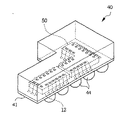
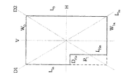
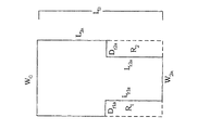
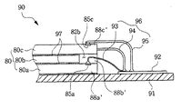
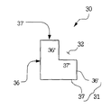
【解決手段】 半導体ダイは、最大幅W0、最大長さL0及び第1凹部Rlを有し、W0において第1凹部深さDrla減少されて第1短軸幅Wlaが形成され、L0において第1凹部長さLrla減少されて第1短軸長さLlaが形成される。
【選択図】 図5A
Description
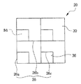
例えば、少なくとも二つのダイの凹部が相互補完的であるか、または外周面に沿って実質的に一定距離を置いて配置され得る。或いは少なくとも二つのダイの凹部が相互補完的でないことも、またダイの外周面の隣接部分に沿って互いに異なる地点から実質的に互に異なる距離へと離隔され得る。
41 基板
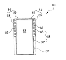
82a,82b,82c 凹部
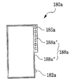
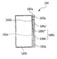
182a 凹部
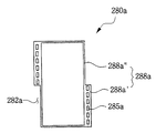
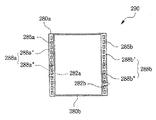
282a,288a 凹部
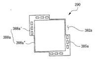
382a,388a 凹部
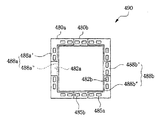
482a,488a 凹部
Claims (34)
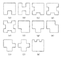
- 変形された矩形の外周を有する半導体ダイにおいて、
最大幅W0と、
最大長さL0と、
第1凹部
とを有し、
前記W0において第1凹部深さDrla減少されて第1短軸幅Wlaが形成され、前記L0において第1凹部長さLrla減少されて第1短軸長さLlaが形成されることを特徴とする半導体ダイ。 - 第2凹部をさらに有し、
前記W0において第2凹部深さDRr2a減少されて第2幅W2aが形成され、前記L0において第2凹部長さLr2a減少されて第2長さL2aが形成されることを特徴とする請求項1に記載の半導体ダイ。 - 偶数個Nの凹部をさらに有し、
前記W0においてN番目凹部深さDrNaに減少されて第N幅WNaが形成され、前記L0がN番目凹部長さLrNaに減少されて第N長さLNaが形成されることを特徴とする請求項2に記載の半導体ダイ。 - 前記N個の凹部は、中心縦軸を基準にして対称に配列することを特徴とする請求項3に記載の半導体ダイ。
- 前記N個の凹部は、中心水平軸を基準にして対称に配列することを特徴とする請求項3に記載の半導体ダイ。
- 前記N個の凹部は、中心縦軸を基準にして対称に配列することを特徴とする請求項5に記載の半導体ダイ。
- 前記N個の凹部は、第1対角線軸を基準にして対称に配列することを特徴とする請求項3に記載の半導体ダイ。
- 前記凹部は、前記半導体ダイの角を取り囲むことを特徴とする請求項1に記載の半導体ダイ。
- 前記凹部は、前記半導体ダイの第1面に沿って中間地点に形成することを特徴とする請求項1に記載の半導体ダイ。
- 前記第1凹部及び第2凹部は、互いに噛み合って前記半導体ダイの一方の角を取り囲むことを特徴とする請求項2に記載の半導体ダイ。
- 前記第1凹部及び第2凹部は、前記半導体ダイの周辺領域により互いに離隔されることを特徴とする請求項2に記載の半導体ダイ。
- 前記第1凹部は、前記半導体ダイの第1角を取り囲み、
前記第2凹部は、前記半導体ダイの第1角と異なる第2角を取り囲むことを特徴とする請求項2に記載の半導体ダイ。 - 前記第1角及び第2角は、対角線に向かい合っていることを特徴とする請求項12に記載の半導体ダイ。
- 前記第1角及び第2角は、前記半導体ダイの一方面の両先端に位置することを特徴とする請求項12に記載の半導体ダイ。
- 外周に凹部が形成された複数のダイを半導体ウエハに形成する段階と、
前記ウエハにおいて個別ダイを分離する段階と
を有することを特徴とする半導体素子製造方法。 - 前記分離段階は、前記ダイの外周面をレーザスクライビングしてウエハで脆弱な部分を形成する段階と、
前記脆弱な部分に沿って隣接するダイから個別ダイを分離する段階と、
を有することを特徴とする請求項15に記載の半導体素子製造方法。 - 前記分離段階は、前記ダイの外周面の外側において前記凹部に近接するするウエハの上部を除去して前記ウエハの活性面に開放口を形成する段階と、
前記活性面の反対面においてウエハの下部を除去して上下部がウエハの元来の厚さと少なくとも同じくする段階と、
ダイ間の切断線に沿って前記ウエハの残り部分を除去する段階と、
を有することを特徴とする請求項15に記載の半導体素子製造方法。 - 半導体ウエハに複数のダイを形成する段階は、隣接する少なくとも二つのダイの凹部が相互補完的でかつダイの外周面に沿って一定間隔に離隔されるようにダイを配列する段階を含むことを特徴とする請求項15に記載の半導体素子製造方法。
- 半導体ウエハに複数のダイを形成する段階は、隣接する少なくとも二つのダイの凹部が完全に相互補完的でなくダイの外周面の隣接部分に沿って互いに異なる地点から互いに異なる間隔に離隔されるようにダイを配列する段階を含むことを特徴とする請求項15に記載の半導体素子製造方法。
- 半導体ウエハに複数のダイを形成する段階は、凹部と境界をなすダイの外周面の一部にはボンドパッドが形成されないように複数のボンドパッドを、ダイの外周面に隣接して配置させる段階を含むことを特徴とする請求項15に記載の半導体素子製造方法。
- 前記複数のボンドパッドは、ダイの外周面の一直線に沿って配列することを特徴とする請求項20に記載の半導体素子製造方法。
- 接触部を有する基板と、
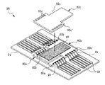
外周面に凹部を有する第1半導体ダイと、
を備える半導体素子パッケージにおいて、
前記接触部が凹部を介して露出するように前記基板に第1半導体ダイを実装することを特徴とする半導体素子パッケージ。 - 前記基板は下部半導体ダイであって、前記接触部は少なくとも一つのボンドパッドを備えて、
複数のボンドパッドは、前記第1半導体ダイの活性面に形成することを特徴とする請求項22に記載の半導体素子パッケージ。 - 前記第1半導体ダイの活性面に形成されるボンドパッドは、延長領域のみに位置することを特徴とする請求項23に記載の半導体素子パッケージ。
- 接触面を有する基板と、
外周面に凹部が形成された第1半導体ダイと、
を備える半導体素子パッケージにおいて、
前記接触部が凹部を介して露出するように前記基板に第1半導体ダイが実装されることを特徴とする請求項22に記載の半導体素子パッケージ。 - 基板を用意する段階と、
前記基板に複数の第1ボンドパッドを有する第1半導体ダイを実装する段階と、
外周面に第1凹部が形成された第2半導体ダイを形成する段階と、
前記複数の第1ボンドパッドが前記第1凹部を介して露出するように前記第1半導体ダイ上に前記第2半導体ダイを実装する段階と、
を有することを特徴とする半導体素子パッケージ製造方法。 - 変形された矩形の外周面に第2凹部が変形されている第3半導体素子を形成する段階と、
前記第2半導体素子の活性面に形成されている複数の第2ボンドパッドが、前記第2凹部を介して露出するように前記第2半導体ダイ上に前記第3半導体ダイを実装する段階と、
をさらに有することを特徴とする半導体素子パッケージ製造方法。 - 前記第1ボンドパッドと第2ボンドパッド及び基板を電気的に接続する段階をさらに有することを特徴とする請求項27に記載の半導体素子パッケージ製造方法。
- 前記第3半導体ダイの活性面に形成されている複数の第3ボンドパッドと基板とを電気的に接続する段階をさらに有することを特徴とする請求項28に記載の半導体素子パッケージ製造方法。
- 前記第1半導体ダイ、第2半導体ダイ及び第3半導体ダイは、実質的に同じ構造を有し、前記第2半導体ダイは、前記第1半導体ダイ及び第3半導体ダイを基準にして約180°回転されることを特徴とする請求項29に記載の半導体素子パッケージ製造方法。
- 前記第1半導体ダイ、第2半導体ダイ及び第3半導体ダイは、実質的に同じ構造を有し、前記第2半導体ダイは、前記第1半導体ダイ及び第3半導体ダイを基準にして約90°回転されることを特徴とする請求項29に記載の半導体素子パッケージ製造方法。
- 少なくとも二つの半導体ダイを備える半導体素子パッケージにおいて、
外周面に凹部が形成されており、基板に実装される第1半導体ダイと、
前記凹部内に位置するように前記第1半導体ダイと水平に実装され第2半導体ダイと、
を備えることを特徴とする半導体素子パッケージ。 - 前記第2半導体ダイは、実質的に前記凹部内に位置することを特徴とする請求項32に記載の半導体素子。
- 前記第2半導体ダイは、前記凹部内に完全に位置することを特徴とする請求項32に記載の半導体素子。
Applications Claiming Priority (2)
| Application Number | Priority Date | Filing Date | Title |
|---|---|---|---|
| KR1020040022666A KR100627006B1 (ko) | 2004-04-01 | 2004-04-01 | 인덴트 칩과, 그를 이용한 반도체 패키지와 멀티 칩 패키지 |
| KR2004-022666 | 2004-04-01 |
Publications (2)
| Publication Number | Publication Date |
|---|---|
| JP2005294842A true JP2005294842A (ja) | 2005-10-20 |
| JP4832782B2 JP4832782B2 (ja) | 2011-12-07 |
Family
ID=34985361
Family Applications (1)
| Application Number | Title | Priority Date | Filing Date |
|---|---|---|---|
| JP2005103706A Expired - Fee Related JP4832782B2 (ja) | 2004-04-01 | 2005-03-31 | 段差型ダイを有する半導体パッケージとその製造方法 |
Country Status (4)
| Country | Link |
|---|---|
| US (1) | US7485955B2 (ja) |
| JP (1) | JP4832782B2 (ja) |
| KR (1) | KR100627006B1 (ja) |
| DE (1) | DE102005016439B4 (ja) |
Cited By (8)
| Publication number | Priority date | Publication date | Assignee | Title |
|---|---|---|---|---|
| JP2011146718A (ja) * | 2010-01-18 | 2011-07-28 | Semiconductor Components Industries Llc | 半導体ダイを形成する方法 |
| JP2011228711A (ja) * | 2010-04-19 | 2011-11-10 | Tokyo Electron Ltd | 半導体集積回路チップを分離および搬送する方法 |
| JP2014017413A (ja) * | 2012-07-10 | 2014-01-30 | Denso Corp | 半導体装置及びその製造方法 |
| JP2014072239A (ja) * | 2012-09-27 | 2014-04-21 | Rohm Co Ltd | チップ部品 |
| US9165833B2 (en) | 2010-01-18 | 2015-10-20 | Semiconductor Components Industries, Llc | Method of forming a semiconductor die |
| US9275957B2 (en) | 2010-01-18 | 2016-03-01 | Semiconductor Components Industries, Llc | EM protected semiconductor die |
| JP2023125523A (ja) * | 2022-02-28 | 2023-09-07 | 三菱電機株式会社 | 半導体装置 |
| JP2023173553A (ja) * | 2022-05-26 | 2023-12-07 | 浜松ホトニクス株式会社 | ウエハ及びウエハの加工方法 |
Families Citing this family (17)
| Publication number | Priority date | Publication date | Assignee | Title |
|---|---|---|---|---|
| US6551857B2 (en) | 1997-04-04 | 2003-04-22 | Elm Technology Corporation | Three dimensional structure integrated circuits |
| US7579681B2 (en) * | 2002-06-11 | 2009-08-25 | Micron Technology, Inc. | Super high density module with integrated wafer level packages |
| AU2003255254A1 (en) | 2002-08-08 | 2004-02-25 | Glenn J. Leedy | Vertical system integration |
| KR100627006B1 (ko) * | 2004-04-01 | 2006-09-25 | 삼성전자주식회사 | 인덴트 칩과, 그를 이용한 반도체 패키지와 멀티 칩 패키지 |
| US7545031B2 (en) * | 2005-04-11 | 2009-06-09 | Stats Chippac Ltd. | Multipackage module having stacked packages with asymmetrically arranged die and molding |
| KR101539402B1 (ko) * | 2008-10-23 | 2015-07-27 | 삼성전자주식회사 | 반도체 패키지 |
| FR2940521B1 (fr) * | 2008-12-19 | 2011-11-11 | 3D Plus | Procede de fabrication collective de modules electroniques pour montage en surface |
| US20110233718A1 (en) * | 2010-03-25 | 2011-09-29 | Qualcomm Incorporated | Heterogeneous Technology Integration |
| JP5995563B2 (ja) * | 2012-07-11 | 2016-09-21 | 株式会社ディスコ | 光デバイスの加工方法 |
| KR101999114B1 (ko) * | 2013-06-03 | 2019-07-11 | 에스케이하이닉스 주식회사 | 반도체 패키지 |
| TWI564997B (zh) * | 2015-06-12 | 2017-01-01 | 萬國半導體股份有限公司 | 功率半導體裝置及其製備方法 |
| US10037946B2 (en) | 2016-02-05 | 2018-07-31 | Dyi-chung Hu | Package structure having embedded bonding film and manufacturing method thereof |
| US9806044B2 (en) * | 2016-02-05 | 2017-10-31 | Dyi-chung Hu | Bonding film for signal communication between central chip and peripheral chips and fabricating method thereof |
| KR102358343B1 (ko) | 2017-08-09 | 2022-02-07 | 삼성전자주식회사 | 반도체 패키지 |
| KR102378837B1 (ko) * | 2018-08-24 | 2022-03-24 | 삼성전자주식회사 | 반도체 장치 및 이를 포함하는 반도체 패키지 |
| US20240006397A1 (en) * | 2022-06-30 | 2024-01-04 | Prilit Optronics, Inc. | Display panel |
| TWI841184B (zh) * | 2023-01-09 | 2024-05-01 | 福懋科技股份有限公司 | 半導體封裝及其製造方法 |
Citations (2)
| Publication number | Priority date | Publication date | Assignee | Title |
|---|---|---|---|---|
| JPH05267449A (ja) * | 1992-03-19 | 1993-10-15 | Mitsubishi Electric Corp | 半導体装置及びその製造方法 |
| JPH11224864A (ja) * | 1998-02-06 | 1999-08-17 | Mitsubishi Electric Corp | 半導体ウエハチップ分離方法 |
Family Cites Families (17)
| Publication number | Priority date | Publication date | Assignee | Title |
|---|---|---|---|---|
| US3538400A (en) | 1967-07-31 | 1970-11-03 | Nippon Electric Co | Semiconductor gunn effect switching element |
| US3816906A (en) | 1969-06-20 | 1974-06-18 | Siemens Ag | Method of dividing mg-al spinel substrate wafers coated with semiconductor material and provided with semiconductor components |
| JPS6193613A (ja) | 1984-10-15 | 1986-05-12 | Nec Corp | 半導体集積回路装置 |
| US5323060A (en) | 1993-06-02 | 1994-06-21 | Micron Semiconductor, Inc. | Multichip module having a stacked chip arrangement |
| JP3007023B2 (ja) | 1995-05-30 | 2000-02-07 | シャープ株式会社 | 半導体集積回路およびその製造方法 |
| KR19980067184A (ko) | 1997-01-31 | 1998-10-15 | 김광호 | 웨이퍼 절단과 다이 본딩이 동시에 이루어지는 인라인 장치 |
| KR19980084225A (ko) | 1997-05-22 | 1998-12-05 | 윤종용 | 반도체 웨이퍼 절단장치 |
| JP3670853B2 (ja) | 1998-07-30 | 2005-07-13 | 三洋電機株式会社 | 半導体装置 |
| JP3643705B2 (ja) | 1998-07-31 | 2005-04-27 | 三洋電機株式会社 | 半導体装置とその製造方法 |
| JP2000306865A (ja) | 1999-02-17 | 2000-11-02 | Toshiba Electronic Engineering Corp | ウェーハ切断方法およびその装置 |
| US6605875B2 (en) | 1999-12-30 | 2003-08-12 | Intel Corporation | Integrated circuit die having bond pads near adjacent sides to allow stacking of dice without regard to dice size |
| JP3832170B2 (ja) | 2000-01-06 | 2006-10-11 | セイコーエプソン株式会社 | マルチベアチップ実装体 |
| US6359340B1 (en) | 2000-07-28 | 2002-03-19 | Advanced Semiconductor Engineering, Inc. | Multichip module having a stacked chip arrangement |
| KR100401020B1 (ko) | 2001-03-09 | 2003-10-08 | 앰코 테크놀로지 코리아 주식회사 | 반도체칩의 스택킹 구조 및 이를 이용한 반도체패키지 |
| KR100407472B1 (ko) | 2001-06-29 | 2003-11-28 | 삼성전자주식회사 | 트렌치가 형성된 상부 칩을 구비하는 칩 적층형 패키지소자 및 그 제조 방법 |
| KR20030075860A (ko) | 2002-03-21 | 2003-09-26 | 삼성전자주식회사 | 반도체 칩 적층 구조 및 적층 방법 |
| KR100627006B1 (ko) * | 2004-04-01 | 2006-09-25 | 삼성전자주식회사 | 인덴트 칩과, 그를 이용한 반도체 패키지와 멀티 칩 패키지 |
-
2004
- 2004-04-01 KR KR1020040022666A patent/KR100627006B1/ko not_active Expired - Fee Related
-
2005
- 2005-03-11 US US11/077,235 patent/US7485955B2/en not_active Expired - Lifetime
- 2005-03-31 JP JP2005103706A patent/JP4832782B2/ja not_active Expired - Fee Related
- 2005-04-01 DE DE102005016439A patent/DE102005016439B4/de not_active Expired - Lifetime
Patent Citations (2)
| Publication number | Priority date | Publication date | Assignee | Title |
|---|---|---|---|---|
| JPH05267449A (ja) * | 1992-03-19 | 1993-10-15 | Mitsubishi Electric Corp | 半導体装置及びその製造方法 |
| JPH11224864A (ja) * | 1998-02-06 | 1999-08-17 | Mitsubishi Electric Corp | 半導体ウエハチップ分離方法 |
Cited By (11)
| Publication number | Priority date | Publication date | Assignee | Title |
|---|---|---|---|---|
| JP2011146718A (ja) * | 2010-01-18 | 2011-07-28 | Semiconductor Components Industries Llc | 半導体ダイを形成する方法 |
| US9165833B2 (en) | 2010-01-18 | 2015-10-20 | Semiconductor Components Industries, Llc | Method of forming a semiconductor die |
| US9275957B2 (en) | 2010-01-18 | 2016-03-01 | Semiconductor Components Industries, Llc | EM protected semiconductor die |
| US9299664B2 (en) | 2010-01-18 | 2016-03-29 | Semiconductor Components Industries, Llc | Method of forming an EM protected semiconductor die |
| US9437493B2 (en) | 2010-01-18 | 2016-09-06 | Semiconductor Components Industries, Llc | Method of forming a semiconductor die |
| JP2011228711A (ja) * | 2010-04-19 | 2011-11-10 | Tokyo Electron Ltd | 半導体集積回路チップを分離および搬送する方法 |
| JP2014017413A (ja) * | 2012-07-10 | 2014-01-30 | Denso Corp | 半導体装置及びその製造方法 |
| JP2014072239A (ja) * | 2012-09-27 | 2014-04-21 | Rohm Co Ltd | チップ部品 |
| JP2023125523A (ja) * | 2022-02-28 | 2023-09-07 | 三菱電機株式会社 | 半導体装置 |
| JP7729235B2 (ja) | 2022-02-28 | 2025-08-26 | 三菱電機株式会社 | 半導体装置 |
| JP2023173553A (ja) * | 2022-05-26 | 2023-12-07 | 浜松ホトニクス株式会社 | ウエハ及びウエハの加工方法 |
Also Published As
| Publication number | Publication date |
|---|---|
| KR100627006B1 (ko) | 2006-09-25 |
| JP4832782B2 (ja) | 2011-12-07 |
| DE102005016439A1 (de) | 2005-10-20 |
| US20050205975A1 (en) | 2005-09-22 |
| DE102005016439B4 (de) | 2011-07-28 |
| US7485955B2 (en) | 2009-02-03 |
| KR20050097586A (ko) | 2005-10-10 |
Similar Documents
| Publication | Publication Date | Title |
|---|---|---|
| JP4832782B2 (ja) | 段差型ダイを有する半導体パッケージとその製造方法 | |
| KR100594229B1 (ko) | 반도체 패키지 및 그 제조방법 | |
| WO2006044804A2 (en) | Multi chip leadframe package | |
| KR20080013305A (ko) | 사이즈가 상이한 복수의 반도체 칩이 적층된 멀티 칩패키지 및 그 제조방법 | |
| JP2003078106A (ja) | チップ積層型パッケージ素子及びその製造方法 | |
| TW201737446A (zh) | 具有多個共面中介元件的半導體封裝 | |
| TWI446461B (zh) | 具有外部互連陣列的積體電路封裝件系統 | |
| CN112670191A (zh) | 半导体封装方法、半导体封装结构及封装体 | |
| CN101447441A (zh) | 包含具有起伏的有源区的芯片的集成电路封装系统 | |
| US20090203171A1 (en) | Semiconductor device fabricating method | |
| KR102739235B1 (ko) | 반도체 패키지 | |
| US20170179101A1 (en) | Bridge structure for embedding semiconductor die | |
| CN100448003C (zh) | 半导体器件 | |
| US9462694B2 (en) | Spacer layer for embedding semiconductor die | |
| JP4497304B2 (ja) | 半導体装置及びその製造方法 | |
| JP2002100707A (ja) | 半導体装置およびその製造方法 | |
| US7445944B2 (en) | Packaging substrate and manufacturing method thereof | |
| TW202230710A (zh) | 半導體封裝以及其製造方法 | |
| TWI883655B (zh) | 半導體裝置及半導體裝置的製造方法 | |
| US20260068740A1 (en) | Semiconductor chip and semiconductor package including the same | |
| CN101609818A (zh) | 半导体封装装置、半导体封装结构及其制法 | |
| CN100378977C (zh) | 无晶片承载件的半导体装置及其制法 | |
| KR100681264B1 (ko) | 전자소자 패키지 및 그의 제조 방법 | |
| TW201236115A (en) | Method for manufacturing semiconductor chips, mounting method and semiconductor chip for vertical mounting onto circuit substrates | |
| KR20240108618A (ko) | 반도체 패키지 및 반도체 패키지의 제조 방법 |
Legal Events
| Date | Code | Title | Description |
|---|---|---|---|
| A621 | Written request for application examination |
Free format text: JAPANESE INTERMEDIATE CODE: A621 Effective date: 20071107 |
|
| A977 | Report on retrieval |
Free format text: JAPANESE INTERMEDIATE CODE: A971007 Effective date: 20100603 |
|
| A131 | Notification of reasons for refusal |
Free format text: JAPANESE INTERMEDIATE CODE: A131 Effective date: 20100608 |
|
| A521 | Request for written amendment filed |
Free format text: JAPANESE INTERMEDIATE CODE: A523 Effective date: 20100907 |
|
| A02 | Decision of refusal |
Free format text: JAPANESE INTERMEDIATE CODE: A02 Effective date: 20110322 |
|
| A521 | Request for written amendment filed |
Free format text: JAPANESE INTERMEDIATE CODE: A523 Effective date: 20110720 |
|
| A911 | Transfer to examiner for re-examination before appeal (zenchi) |
Free format text: JAPANESE INTERMEDIATE CODE: A911 Effective date: 20110801 |
|
| TRDD | Decision of grant or rejection written | ||
| A01 | Written decision to grant a patent or to grant a registration (utility model) |
Free format text: JAPANESE INTERMEDIATE CODE: A01 Effective date: 20110823 |
|
| A01 | Written decision to grant a patent or to grant a registration (utility model) |
Free format text: JAPANESE INTERMEDIATE CODE: A01 |
|
| A61 | First payment of annual fees (during grant procedure) |
Free format text: JAPANESE INTERMEDIATE CODE: A61 Effective date: 20110921 |
|
| R150 | Certificate of patent or registration of utility model |
Ref document number: 4832782 Country of ref document: JP Free format text: JAPANESE INTERMEDIATE CODE: R150 |
|
| FPAY | Renewal fee payment (event date is renewal date of database) |
Free format text: PAYMENT UNTIL: 20140930 Year of fee payment: 3 |
|
| R250 | Receipt of annual fees |
Free format text: JAPANESE INTERMEDIATE CODE: R250 |
|
| R250 | Receipt of annual fees |
Free format text: JAPANESE INTERMEDIATE CODE: R250 |
|
| R250 | Receipt of annual fees |
Free format text: JAPANESE INTERMEDIATE CODE: R250 |
|
| R250 | Receipt of annual fees |
Free format text: JAPANESE INTERMEDIATE CODE: R250 |
|
| R250 | Receipt of annual fees |
Free format text: JAPANESE INTERMEDIATE CODE: R250 |
|
| R250 | Receipt of annual fees |
Free format text: JAPANESE INTERMEDIATE CODE: R250 |
|
| R250 | Receipt of annual fees |
Free format text: JAPANESE INTERMEDIATE CODE: R250 |
|
| R250 | Receipt of annual fees |
Free format text: JAPANESE INTERMEDIATE CODE: R250 |
|
| R250 | Receipt of annual fees |
Free format text: JAPANESE INTERMEDIATE CODE: R250 |
|
| R250 | Receipt of annual fees |
Free format text: JAPANESE INTERMEDIATE CODE: R250 |
|
| LAPS | Cancellation because of no payment of annual fees |