JP2005294842A - Semiconductor package having step type die and method of manufacturing the same - Google Patents
Semiconductor package having step type die and method of manufacturing the same Download PDFInfo
- Publication number
- JP2005294842A JP2005294842A JP2005103706A JP2005103706A JP2005294842A JP 2005294842 A JP2005294842 A JP 2005294842A JP 2005103706 A JP2005103706 A JP 2005103706A JP 2005103706 A JP2005103706 A JP 2005103706A JP 2005294842 A JP2005294842 A JP 2005294842A
- Authority
- JP
- Japan
- Prior art keywords
- semiconductor die
- recess
- semiconductor
- die
- substrate
- Prior art date
- Legal status (The legal status is an assumption and is not a legal conclusion. Google has not performed a legal analysis and makes no representation as to the accuracy of the status listed.)
- Granted
Links
Images


Classifications
-
- A—HUMAN NECESSITIES
- A23—FOODS OR FOODSTUFFS; TREATMENT THEREOF, NOT COVERED BY OTHER CLASSES
- A23N—MACHINES OR APPARATUS FOR TREATING HARVESTED FRUIT, VEGETABLES OR FLOWER BULBS IN BULK, NOT OTHERWISE PROVIDED FOR; PEELING VEGETABLES OR FRUIT IN BULK; APPARATUS FOR PREPARING ANIMAL FEEDING- STUFFS
- A23N15/00—Machines or apparatus for other treatment of fruits or vegetables for human purposes; Machines or apparatus for topping or skinning flower bulbs
-
- H—ELECTRICITY
- H10—SEMICONDUCTOR DEVICES; ELECTRIC SOLID-STATE DEVICES NOT OTHERWISE PROVIDED FOR
- H10D—INORGANIC ELECTRIC SEMICONDUCTOR DEVICES
- H10D62/00—Semiconductor bodies, or regions thereof, of devices having potential barriers
- H10D62/10—Shapes, relative sizes or dispositions of the regions of the semiconductor bodies; Shapes of the semiconductor bodies
- H10D62/117—Shapes of semiconductor bodies
-
- B—PERFORMING OPERATIONS; TRANSPORTING
- B26—HAND CUTTING TOOLS; CUTTING; SEVERING
- B26D—CUTTING; DETAILS COMMON TO MACHINES FOR PERFORATING, PUNCHING, CUTTING-OUT, STAMPING-OUT OR SEVERING
- B26D3/00—Cutting work characterised by the nature of the cut made; Apparatus therefor
- B26D3/24—Cutting work characterised by the nature of the cut made; Apparatus therefor to obtain segments other than slices, e.g. cutting pies
- B26D3/26—Cutting work characterised by the nature of the cut made; Apparatus therefor to obtain segments other than slices, e.g. cutting pies specially adapted for cutting fruit or vegetables, e.g. for onions
-
- B—PERFORMING OPERATIONS; TRANSPORTING
- B26—HAND CUTTING TOOLS; CUTTING; SEVERING
- B26D—CUTTING; DETAILS COMMON TO MACHINES FOR PERFORATING, PUNCHING, CUTTING-OUT, STAMPING-OUT OR SEVERING
- B26D5/00—Arrangements for operating and controlling machines or devices for cutting, cutting-out, stamping-out, punching, perforating, or severing by means other than cutting
- B26D5/08—Means for actuating the cutting member to effect the cut
- B26D5/086—Electric, magnetic, piezoelectric, electro-magnetic means
-
- B—PERFORMING OPERATIONS; TRANSPORTING
- B26—HAND CUTTING TOOLS; CUTTING; SEVERING
- B26D—CUTTING; DETAILS COMMON TO MACHINES FOR PERFORATING, PUNCHING, CUTTING-OUT, STAMPING-OUT OR SEVERING
- B26D7/00—Details of apparatus for cutting, cutting-out, stamping-out, punching, perforating, or severing by means other than cutting
- B26D7/06—Arrangements for feeding or delivering work of other than sheet, web, or filamentary form
- B26D7/0625—Arrangements for feeding or delivering work of other than sheet, web, or filamentary form by endless conveyors, e.g. belts
-
- B—PERFORMING OPERATIONS; TRANSPORTING
- B26—HAND CUTTING TOOLS; CUTTING; SEVERING
- B26D—CUTTING; DETAILS COMMON TO MACHINES FOR PERFORATING, PUNCHING, CUTTING-OUT, STAMPING-OUT OR SEVERING
- B26D7/00—Details of apparatus for cutting, cutting-out, stamping-out, punching, perforating, or severing by means other than cutting
- B26D7/06—Arrangements for feeding or delivering work of other than sheet, web, or filamentary form
- B26D7/0641—Arrangements for feeding or delivering work of other than sheet, web, or filamentary form using chutes, hoppers, magazines
-
- B—PERFORMING OPERATIONS; TRANSPORTING
- B26—HAND CUTTING TOOLS; CUTTING; SEVERING
- B26D—CUTTING; DETAILS COMMON TO MACHINES FOR PERFORATING, PUNCHING, CUTTING-OUT, STAMPING-OUT OR SEVERING
- B26D7/00—Details of apparatus for cutting, cutting-out, stamping-out, punching, perforating, or severing by means other than cutting
- B26D7/18—Means for removing cut-out material or waste
-
- H—ELECTRICITY
- H10—SEMICONDUCTOR DEVICES; ELECTRIC SOLID-STATE DEVICES NOT OTHERWISE PROVIDED FOR
- H10P—GENERIC PROCESSES OR APPARATUS FOR THE MANUFACTURE OR TREATMENT OF DEVICES COVERED BY CLASS H10
- H10P54/00—Cutting or separating of wafers, substrates or parts of devices
-
- H—ELECTRICITY
- H10—SEMICONDUCTOR DEVICES; ELECTRIC SOLID-STATE DEVICES NOT OTHERWISE PROVIDED FOR
- H10W—GENERIC PACKAGES, INTERCONNECTIONS, CONNECTORS OR OTHER CONSTRUCTIONAL DETAILS OF DEVICES COVERED BY CLASS H10
- H10W74/00—Encapsulations, e.g. protective coatings
- H10W74/10—Encapsulations, e.g. protective coatings characterised by their shape or disposition
- H10W74/111—Encapsulations, e.g. protective coatings characterised by their shape or disposition the semiconductor body being completely enclosed
- H10W74/114—Encapsulations, e.g. protective coatings characterised by their shape or disposition the semiconductor body being completely enclosed by a substrate and the encapsulations
- H10W74/117—Encapsulations, e.g. protective coatings characterised by their shape or disposition the semiconductor body being completely enclosed by a substrate and the encapsulations the substrate having spherical bumps for external connection
-
- H—ELECTRICITY
- H10—SEMICONDUCTOR DEVICES; ELECTRIC SOLID-STATE DEVICES NOT OTHERWISE PROVIDED FOR
- H10W—GENERIC PACKAGES, INTERCONNECTIONS, CONNECTORS OR OTHER CONSTRUCTIONAL DETAILS OF DEVICES COVERED BY CLASS H10
- H10W90/00—Package configurations
-
- A—HUMAN NECESSITIES
- A23—FOODS OR FOODSTUFFS; TREATMENT THEREOF, NOT COVERED BY OTHER CLASSES
- A23N—MACHINES OR APPARATUS FOR TREATING HARVESTED FRUIT, VEGETABLES OR FLOWER BULBS IN BULK, NOT OTHERWISE PROVIDED FOR; PEELING VEGETABLES OR FRUIT IN BULK; APPARATUS FOR PREPARING ANIMAL FEEDING- STUFFS
- A23N15/00—Machines or apparatus for other treatment of fruits or vegetables for human purposes; Machines or apparatus for topping or skinning flower bulbs
- A23N2015/008—Sorting of fruit and vegetables
-
- B—PERFORMING OPERATIONS; TRANSPORTING
- B26—HAND CUTTING TOOLS; CUTTING; SEVERING
- B26D—CUTTING; DETAILS COMMON TO MACHINES FOR PERFORATING, PUNCHING, CUTTING-OUT, STAMPING-OUT OR SEVERING
- B26D2210/00—Machines or methods used for cutting special materials
- B26D2210/02—Machines or methods used for cutting special materials for cutting food products, e.g. food slicers
-
- H—ELECTRICITY
- H10—SEMICONDUCTOR DEVICES; ELECTRIC SOLID-STATE DEVICES NOT OTHERWISE PROVIDED FOR
- H10W—GENERIC PACKAGES, INTERCONNECTIONS, CONNECTORS OR OTHER CONSTRUCTIONAL DETAILS OF DEVICES COVERED BY CLASS H10
- H10W72/00—Interconnections or connectors in packages
- H10W72/071—Connecting or disconnecting
- H10W72/073—Connecting or disconnecting of die-attach connectors
-
- H—ELECTRICITY
- H10—SEMICONDUCTOR DEVICES; ELECTRIC SOLID-STATE DEVICES NOT OTHERWISE PROVIDED FOR
- H10W—GENERIC PACKAGES, INTERCONNECTIONS, CONNECTORS OR OTHER CONSTRUCTIONAL DETAILS OF DEVICES COVERED BY CLASS H10
- H10W72/00—Interconnections or connectors in packages
- H10W72/071—Connecting or disconnecting
- H10W72/075—Connecting or disconnecting of bond wires
- H10W72/07511—Treating the bonding area before connecting, e.g. by applying flux or cleaning
-
- H—ELECTRICITY
- H10—SEMICONDUCTOR DEVICES; ELECTRIC SOLID-STATE DEVICES NOT OTHERWISE PROVIDED FOR
- H10W—GENERIC PACKAGES, INTERCONNECTIONS, CONNECTORS OR OTHER CONSTRUCTIONAL DETAILS OF DEVICES COVERED BY CLASS H10
- H10W72/00—Interconnections or connectors in packages
- H10W72/071—Connecting or disconnecting
- H10W72/075—Connecting or disconnecting of bond wires
- H10W72/07521—Aligning
-
- H—ELECTRICITY
- H10—SEMICONDUCTOR DEVICES; ELECTRIC SOLID-STATE DEVICES NOT OTHERWISE PROVIDED FOR
- H10W—GENERIC PACKAGES, INTERCONNECTIONS, CONNECTORS OR OTHER CONSTRUCTIONAL DETAILS OF DEVICES COVERED BY CLASS H10
- H10W72/00—Interconnections or connectors in packages
- H10W72/071—Connecting or disconnecting
- H10W72/075—Connecting or disconnecting of bond wires
- H10W72/07541—Controlling the environment, e.g. atmosphere composition or temperature
- H10W72/07553—Controlling the environment, e.g. atmosphere composition or temperature changes in shapes
-
- H—ELECTRICITY
- H10—SEMICONDUCTOR DEVICES; ELECTRIC SOLID-STATE DEVICES NOT OTHERWISE PROVIDED FOR
- H10W—GENERIC PACKAGES, INTERCONNECTIONS, CONNECTORS OR OTHER CONSTRUCTIONAL DETAILS OF DEVICES COVERED BY CLASS H10
- H10W72/00—Interconnections or connectors in packages
- H10W72/20—Bump connectors, e.g. solder bumps or copper pillars; Dummy bumps; Thermal bumps
- H10W72/29—Bond pads specially adapted therefor
-
- H—ELECTRICITY
- H10—SEMICONDUCTOR DEVICES; ELECTRIC SOLID-STATE DEVICES NOT OTHERWISE PROVIDED FOR
- H10W—GENERIC PACKAGES, INTERCONNECTIONS, CONNECTORS OR OTHER CONSTRUCTIONAL DETAILS OF DEVICES COVERED BY CLASS H10
- H10W72/00—Interconnections or connectors in packages
- H10W72/50—Bond wires
- H10W72/531—Shapes of wire connectors
- H10W72/536—Shapes of wire connectors the connected ends being ball-shaped
-
- H—ELECTRICITY
- H10—SEMICONDUCTOR DEVICES; ELECTRIC SOLID-STATE DEVICES NOT OTHERWISE PROVIDED FOR
- H10W—GENERIC PACKAGES, INTERCONNECTIONS, CONNECTORS OR OTHER CONSTRUCTIONAL DETAILS OF DEVICES COVERED BY CLASS H10
- H10W72/00—Interconnections or connectors in packages
- H10W72/50—Bond wires
- H10W72/531—Shapes of wire connectors
- H10W72/5363—Shapes of wire connectors the connected ends being wedge-shaped
-
- H—ELECTRICITY
- H10—SEMICONDUCTOR DEVICES; ELECTRIC SOLID-STATE DEVICES NOT OTHERWISE PROVIDED FOR
- H10W—GENERIC PACKAGES, INTERCONNECTIONS, CONNECTORS OR OTHER CONSTRUCTIONAL DETAILS OF DEVICES COVERED BY CLASS H10
- H10W72/00—Interconnections or connectors in packages
- H10W72/50—Bond wires
- H10W72/531—Shapes of wire connectors
- H10W72/5366—Shapes of wire connectors the bond wires having kinks
-
- H—ELECTRICITY
- H10—SEMICONDUCTOR DEVICES; ELECTRIC SOLID-STATE DEVICES NOT OTHERWISE PROVIDED FOR
- H10W—GENERIC PACKAGES, INTERCONNECTIONS, CONNECTORS OR OTHER CONSTRUCTIONAL DETAILS OF DEVICES COVERED BY CLASS H10
- H10W72/00—Interconnections or connectors in packages
- H10W72/50—Bond wires
- H10W72/531—Shapes of wire connectors
- H10W72/537—Multiple bond wires having different shapes
-
- H—ELECTRICITY
- H10—SEMICONDUCTOR DEVICES; ELECTRIC SOLID-STATE DEVICES NOT OTHERWISE PROVIDED FOR
- H10W—GENERIC PACKAGES, INTERCONNECTIONS, CONNECTORS OR OTHER CONSTRUCTIONAL DETAILS OF DEVICES COVERED BY CLASS H10
- H10W72/00—Interconnections or connectors in packages
- H10W72/50—Bond wires
- H10W72/541—Dispositions of bond wires
- H10W72/5434—Dispositions of bond wires the connected ends being on auxiliary connecting means on bond pads, e.g. on other bond wires
-
- H—ELECTRICITY
- H10—SEMICONDUCTOR DEVICES; ELECTRIC SOLID-STATE DEVICES NOT OTHERWISE PROVIDED FOR
- H10W—GENERIC PACKAGES, INTERCONNECTIONS, CONNECTORS OR OTHER CONSTRUCTIONAL DETAILS OF DEVICES COVERED BY CLASS H10
- H10W72/00—Interconnections or connectors in packages
- H10W72/50—Bond wires
- H10W72/541—Dispositions of bond wires
- H10W72/5445—Dispositions of bond wires being orthogonal to a side surface of the chip, e.g. parallel arrangements
-
- H—ELECTRICITY
- H10—SEMICONDUCTOR DEVICES; ELECTRIC SOLID-STATE DEVICES NOT OTHERWISE PROVIDED FOR
- H10W—GENERIC PACKAGES, INTERCONNECTIONS, CONNECTORS OR OTHER CONSTRUCTIONAL DETAILS OF DEVICES COVERED BY CLASS H10
- H10W72/00—Interconnections or connectors in packages
- H10W72/50—Bond wires
- H10W72/59—Bond pads specially adapted therefor
-
- H—ELECTRICITY
- H10—SEMICONDUCTOR DEVICES; ELECTRIC SOLID-STATE DEVICES NOT OTHERWISE PROVIDED FOR
- H10W—GENERIC PACKAGES, INTERCONNECTIONS, CONNECTORS OR OTHER CONSTRUCTIONAL DETAILS OF DEVICES COVERED BY CLASS H10
- H10W72/00—Interconnections or connectors in packages
- H10W72/851—Dispositions of multiple connectors or interconnections
- H10W72/874—On different surfaces
- H10W72/884—Die-attach connectors and bond wires
-
- H—ELECTRICITY
- H10—SEMICONDUCTOR DEVICES; ELECTRIC SOLID-STATE DEVICES NOT OTHERWISE PROVIDED FOR
- H10W—GENERIC PACKAGES, INTERCONNECTIONS, CONNECTORS OR OTHER CONSTRUCTIONAL DETAILS OF DEVICES COVERED BY CLASS H10
- H10W72/00—Interconnections or connectors in packages
- H10W72/90—Bond pads, in general
- H10W72/931—Shapes of bond pads
- H10W72/932—Plan-view shape, i.e. in top view
-
- H—ELECTRICITY
- H10—SEMICONDUCTOR DEVICES; ELECTRIC SOLID-STATE DEVICES NOT OTHERWISE PROVIDED FOR
- H10W—GENERIC PACKAGES, INTERCONNECTIONS, CONNECTORS OR OTHER CONSTRUCTIONAL DETAILS OF DEVICES COVERED BY CLASS H10
- H10W72/00—Interconnections or connectors in packages
- H10W72/90—Bond pads, in general
- H10W72/931—Shapes of bond pads
- H10W72/934—Cross-sectional shape, i.e. in side view
-
- H—ELECTRICITY
- H10—SEMICONDUCTOR DEVICES; ELECTRIC SOLID-STATE DEVICES NOT OTHERWISE PROVIDED FOR
- H10W—GENERIC PACKAGES, INTERCONNECTIONS, CONNECTORS OR OTHER CONSTRUCTIONAL DETAILS OF DEVICES COVERED BY CLASS H10
- H10W72/00—Interconnections or connectors in packages
- H10W72/90—Bond pads, in general
- H10W72/951—Materials of bond pads
-
- H—ELECTRICITY
- H10—SEMICONDUCTOR DEVICES; ELECTRIC SOLID-STATE DEVICES NOT OTHERWISE PROVIDED FOR
- H10W—GENERIC PACKAGES, INTERCONNECTIONS, CONNECTORS OR OTHER CONSTRUCTIONAL DETAILS OF DEVICES COVERED BY CLASS H10
- H10W74/00—Encapsulations, e.g. protective coatings
-
- H—ELECTRICITY
- H10—SEMICONDUCTOR DEVICES; ELECTRIC SOLID-STATE DEVICES NOT OTHERWISE PROVIDED FOR
- H10W—GENERIC PACKAGES, INTERCONNECTIONS, CONNECTORS OR OTHER CONSTRUCTIONAL DETAILS OF DEVICES COVERED BY CLASS H10
- H10W74/00—Encapsulations, e.g. protective coatings
- H10W74/10—Encapsulations, e.g. protective coatings characterised by their shape or disposition
- H10W74/15—Encapsulations, e.g. protective coatings characterised by their shape or disposition on active surfaces of flip-chip devices, e.g. underfills
-
- H—ELECTRICITY
- H10—SEMICONDUCTOR DEVICES; ELECTRIC SOLID-STATE DEVICES NOT OTHERWISE PROVIDED FOR
- H10W—GENERIC PACKAGES, INTERCONNECTIONS, CONNECTORS OR OTHER CONSTRUCTIONAL DETAILS OF DEVICES COVERED BY CLASS H10
- H10W90/00—Package configurations
- H10W90/20—Configurations of stacked chips
-
- H—ELECTRICITY
- H10—SEMICONDUCTOR DEVICES; ELECTRIC SOLID-STATE DEVICES NOT OTHERWISE PROVIDED FOR
- H10W—GENERIC PACKAGES, INTERCONNECTIONS, CONNECTORS OR OTHER CONSTRUCTIONAL DETAILS OF DEVICES COVERED BY CLASS H10
- H10W90/00—Package configurations
- H10W90/20—Configurations of stacked chips
- H10W90/24—Configurations of stacked chips at least one of the stacked chips being laterally offset from a neighbouring stacked chip, e.g. chip stacks having a staircase shape
-
- H—ELECTRICITY
- H10—SEMICONDUCTOR DEVICES; ELECTRIC SOLID-STATE DEVICES NOT OTHERWISE PROVIDED FOR
- H10W—GENERIC PACKAGES, INTERCONNECTIONS, CONNECTORS OR OTHER CONSTRUCTIONAL DETAILS OF DEVICES COVERED BY CLASS H10
- H10W90/00—Package configurations
- H10W90/20—Configurations of stacked chips
- H10W90/291—Configurations of stacked chips characterised by containers, encapsulations, or other housings for the stacked chips
-
- H—ELECTRICITY
- H10—SEMICONDUCTOR DEVICES; ELECTRIC SOLID-STATE DEVICES NOT OTHERWISE PROVIDED FOR
- H10W—GENERIC PACKAGES, INTERCONNECTIONS, CONNECTORS OR OTHER CONSTRUCTIONAL DETAILS OF DEVICES COVERED BY CLASS H10
- H10W90/00—Package configurations
- H10W90/701—Package configurations characterised by the relative positions of pads or connectors relative to package parts
- H10W90/721—Package configurations characterised by the relative positions of pads or connectors relative to package parts of bump connectors
- H10W90/724—Package configurations characterised by the relative positions of pads or connectors relative to package parts of bump connectors between a chip and a stacked insulating package substrate, interposer or RDL
-
- H—ELECTRICITY
- H10—SEMICONDUCTOR DEVICES; ELECTRIC SOLID-STATE DEVICES NOT OTHERWISE PROVIDED FOR
- H10W—GENERIC PACKAGES, INTERCONNECTIONS, CONNECTORS OR OTHER CONSTRUCTIONAL DETAILS OF DEVICES COVERED BY CLASS H10
- H10W90/00—Package configurations
- H10W90/701—Package configurations characterised by the relative positions of pads or connectors relative to package parts
- H10W90/731—Package configurations characterised by the relative positions of pads or connectors relative to package parts of die-attach connectors
- H10W90/732—Package configurations characterised by the relative positions of pads or connectors relative to package parts of die-attach connectors between stacked chips
-
- H—ELECTRICITY
- H10—SEMICONDUCTOR DEVICES; ELECTRIC SOLID-STATE DEVICES NOT OTHERWISE PROVIDED FOR
- H10W—GENERIC PACKAGES, INTERCONNECTIONS, CONNECTORS OR OTHER CONSTRUCTIONAL DETAILS OF DEVICES COVERED BY CLASS H10
- H10W90/00—Package configurations
- H10W90/701—Package configurations characterised by the relative positions of pads or connectors relative to package parts
- H10W90/731—Package configurations characterised by the relative positions of pads or connectors relative to package parts of die-attach connectors
- H10W90/734—Package configurations characterised by the relative positions of pads or connectors relative to package parts of die-attach connectors between a chip and a stacked insulating package substrate, interposer or RDL
-
- H—ELECTRICITY
- H10—SEMICONDUCTOR DEVICES; ELECTRIC SOLID-STATE DEVICES NOT OTHERWISE PROVIDED FOR
- H10W—GENERIC PACKAGES, INTERCONNECTIONS, CONNECTORS OR OTHER CONSTRUCTIONAL DETAILS OF DEVICES COVERED BY CLASS H10
- H10W90/00—Package configurations
- H10W90/701—Package configurations characterised by the relative positions of pads or connectors relative to package parts
- H10W90/751—Package configurations characterised by the relative positions of pads or connectors relative to package parts of bond wires
- H10W90/754—Package configurations characterised by the relative positions of pads or connectors relative to package parts of bond wires between a chip and a stacked insulating package substrate, interposer or RDL
-
- H—ELECTRICITY
- H10—SEMICONDUCTOR DEVICES; ELECTRIC SOLID-STATE DEVICES NOT OTHERWISE PROVIDED FOR
- H10W—GENERIC PACKAGES, INTERCONNECTIONS, CONNECTORS OR OTHER CONSTRUCTIONAL DETAILS OF DEVICES COVERED BY CLASS H10
- H10W90/00—Package configurations
- H10W90/701—Package configurations characterised by the relative positions of pads or connectors relative to package parts
- H10W90/751—Package configurations characterised by the relative positions of pads or connectors relative to package parts of bond wires
- H10W90/756—Package configurations characterised by the relative positions of pads or connectors relative to package parts of bond wires between a chip and a stacked lead frame, conducting package substrate or heat sink
Landscapes
- Life Sciences & Earth Sciences (AREA)
- Engineering & Computer Science (AREA)
- Forests & Forestry (AREA)
- Mechanical Engineering (AREA)
- Chemical & Material Sciences (AREA)
- Food Science & Technology (AREA)
- Polymers & Plastics (AREA)
- Structures Or Materials For Encapsulating Or Coating Semiconductor Devices Or Solid State Devices (AREA)
- Wire Bonding (AREA)
- Dicing (AREA)
- Die Bonding (AREA)
Abstract
Description
本発明は、半導体集積回路チップと、それを用いたパッケージング組立に関し、さらに詳細には変形された矩形の外周面を有する集積回路チップまたはダイ及びそれを一つ以上用いて具現された関連チップまたはマルチチップパッケージに関する。 The present invention relates to a semiconductor integrated circuit chip and a packaging assembly using the semiconductor integrated circuit chip. More specifically, the present invention relates to an integrated circuit chip or die having a deformed rectangular outer peripheral surface and a related chip embodied by using one or more thereof. Or relates to a multi-chip package.
一般に、半導体パッケージの製造工程には、半導体ウエハ加工、パッケージ組立及びテスト等の三つに大別することができる。ウエハ加工工程は、熱処理、イオン注入、蒸着、平坦化、フォトリソグラフィ及びエッチングなどのようなベア半導体ウエハや基板の中または表面に複数の集積回路素子を作る上必要なあらゆる工程を含む。 In general, the manufacturing process of a semiconductor package can be roughly divided into three processes such as semiconductor wafer processing, package assembly, and testing. The wafer processing process includes all processes necessary for forming a plurality of integrated circuit elements in or on a bare semiconductor wafer or substrate, such as heat treatment, ion implantation, vapor deposition, planarization, photolithography and etching.
当該工程が完了すると、パラメータ及び/または機能テストを行った後ウエハダイシング工程に移行する。この工程の間、半導体ウエハの背面が練磨され厚さが減少し、切断線に沿って個別集積回路チップに分離される。このため、ウエハダイシング工程のことを、例えば、ウエハソーイングまたはウエハスクライビング工程ともいう。 When the process is completed, the process proceeds to a wafer dicing process after performing parameter and / or function tests. During this process, the backside of the semiconductor wafer is polished to reduce the thickness and separated into individual integrated circuit chips along the cutting line. For this reason, the wafer dicing process is also referred to as, for example, a wafer sawing or wafer scribing process.
一旦ウエハから個別集積回路チップが分離されると、それぞれの個別集積回路チップをリードフレームの等の基板に取り付けるといったパッケージ組立工程を行うが、基板は、集積回路チップ、回路基板、またはソケットと連結するための外部連結構造を含む。直接回路チップ、基板の一部、及びチップと基板との間の電気的連結部を封止する封止部を形成し、パッケージの抵抗性を増加させることによって、外部による機械的損傷や汚染から保護する。パッケージは、一つ以上の集積回路チップを有するが、マルチチップパッケージの場合、実質的に同じチップを含むか或いは多様な機能や大きさを有するチップを含むことができる。例えば、マルチチップパッケージは、一つのパッケージ内にマイクロプロセッサー集積回路チップとそれと連結されているメモリチップの両方を含んで構成される。 Once the individual integrated circuit chips are separated from the wafer, a package assembly process is performed in which each individual integrated circuit chip is attached to a substrate such as a lead frame. The substrate is connected to the integrated circuit chip, the circuit substrate, or the socket. Including an external connection structure. By forming a sealing part that directly seals the circuit chip, part of the substrate, and the electrical connection between the chip and the substrate, and increases the resistance of the package, from external mechanical damage and contamination Protect. The package includes one or more integrated circuit chips. However, in the case of a multi-chip package, the package may include substantially the same chip or may include chips having various functions and sizes. For example, a multi-chip package is configured to include both a microprocessor integrated circuit chip and a memory chip connected thereto in one package.
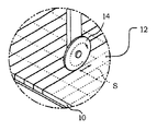
現在、半導体チップの大部分は、図1に示すように、矩形を有するが、これは、従来のウエハダイシング方法に由来する。従来の一般的なウエハダイシング装置は、ダイシングブレード(dicing blade)14を用いてウエハ10上に形成された複数の半導体チップ12間の切断線Sに沿って移動する。ダイシングブレード14の切断長さが集積回路チップ12の表面長さと略同じであることから、従来のダイシング装置では、単純で一定した矩形にしか切断できず、例えば、三角や平行四辺形の形態がなかった。
Currently, most of the semiconductor chips have a rectangular shape as shown in FIG. 1, which is derived from a conventional wafer dicing method. A conventional general wafer dicing apparatus moves along a cutting line S between a plurality of
また、従来のダイシングブレード使用による収率及び/または信頼性を減少させる原因となるチッピング(chipping)といった問題点を解決するために、レーザスクライブを用いたダイシング方法が米国特許出願第10/805、212号に開示されている。さらに、東京精密株式会社のレーザスクライビング装置であるマホウダイシング装置(Mahoh dicing machine)は、従来のソーイングによるウエハ表面の損傷を減す非接触方法を用いて半導体ウエハをダイシングする。半導体ウエハ表面にレーザダイのレーザビームを照射して多様な形態の集積回路チップを切断する。これにより、従来のソーイング方法における研磨材によるウエハの一部を除去する際発生するチッピング等の損傷を減らすことができる。 In addition, in order to solve the problem of chipping that causes a decrease in yield and / or reliability due to the use of a conventional dicing blade, a dicing method using laser scribing is disclosed in US Patent Application No. 10/805, No. 212 is disclosed. Further, a Mahoh dicing machine, which is a laser scribing device of Tokyo Seimitsu Co., Ltd., dices a semiconductor wafer using a non-contact method that reduces damage to the wafer surface due to conventional sawing. Various types of integrated circuit chips are cut by irradiating the surface of a semiconductor wafer with a laser beam of a laser die. This can reduce damage such as chipping that occurs when a part of the wafer is removed by the abrasive in the conventional sawing method.
集積回路チップの矩形は、具現される半導体パッケージの形態も限定しているためパッケージもやはり矩形が圧倒的に多い。このために、複数のパッケージが回路基板と同じ基板に実装されるとき、パッケージの実装密度が減少するとともに集積回路チップの実装に必要な基板の大きさが増大する。 The rectangle of the integrated circuit chip limits the form of the semiconductor package to be implemented, so that the package is also predominantly rectangular. For this reason, when a plurality of packages are mounted on the same substrate as the circuit board, the packaging density of the package is reduced and the size of the board necessary for mounting the integrated circuit chip is increased.
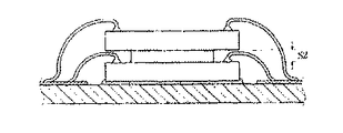
また、集積回路チップの矩形は、マルチチップパッケージの小型・薄型形状にすることが困難である。例えば、二つの集積回路チップが積層されると、上部チップの大きさが下部チップのボンドパッドを覆う程度であれば、集積回路チップ間にスペーサが介在され下部チップのボンドパッドに接近可能な空間を作らなければならない。しかし、図3Aに示すように、スペーサの介在により積層チップの厚さがS2にまで増大してしまう。 Further, it is difficult to make the rectangular shape of the integrated circuit chip into a small and thin shape of the multichip package. For example, when two integrated circuit chips are stacked, if the size of the upper chip is sufficient to cover the bond pad of the lower chip, a space is interposed between the integrated circuit chips and is accessible to the bond pad of the lower chip. Must be made. However, as shown in FIG. 3A, the thickness of the multilayer chip increases to S2 due to the spacer.
上下部チップ間の干渉を解決するための方法の一つとして、図3Bに示すように、上部チップの下部面端部を除去して下部チップのボンドパッドにワイヤボンディングできる大きさの五目型開放部を形成する方法がある。しかし、この方法は、上部チップの一部が薄形化されてしまうことから、ワイヤボンディングの際弱くなった箇所が折れたりクラックが発生したりする恐れがある。 As one method for solving the interference between the upper and lower chips, as shown in FIG. 3B, the lower surface end portion of the upper chip is removed, and a five-eye type opening that can be bonded to the bond pad of the lower chip is opened. There is a method of forming a part. However, in this method, since a part of the upper chip is thinned, there is a possibility that a weakened part is broken or a crack is generated at the time of wire bonding.
下部チップのボンドパッドを覆う方法の一つとして、下部チップを基準にして上部チップを回転させて対角方向に実装し、下部チップにワイヤボンディング領域を露出する方法がある。この方法は、チップの一部が機械的損傷の危険に晒されないものの下部チップのボンドパッドに接近性を向上させるために、大きさ及び方向の異なるチップを用いなければならないという制限があり、さらにオフセット配列のために装置及び/または制御装置を使用しなければならない問題点があった。 As one method of covering the bond pads of the lower chip, there is a method in which the upper chip is rotated with respect to the lower chip and mounted diagonally, and the wire bonding area is exposed on the lower chip. This method has the limitation that chips of different sizes and orientations must be used to improve accessibility to the bond pads of the lower chip, although some of the chips are not at risk of mechanical damage, There was a problem that the device and / or control device had to be used for the offset arrangement.
本発明の目的は、一つ以上の凹部を有しながら外周面が矩形以外の多様な形態の集積回路チップを提供し、それに具現されるチップ及びマルチチップパッケージを提供することにある。 SUMMARY OF THE INVENTION An object of the present invention is to provide an integrated circuit chip having various forms other than a rectangular outer peripheral surface having one or more recesses, and to provide a chip and a multichip package embodied therein.
上記目的を達成するために、本発明は、最大幅W0と最大長さL0を含む変形された矩形の外周を有する半導体ダイを提供する。一面に沿って角まで凹部が形成されており、元来の幅から第1凹部深さDr1aに減少されて第1部方幅Wlaを形成し、元来の長さL0から第1凹部長さLr1aに減少されて第1部方長さL1aが形成される。本発明による集積回路チップにおいて凹部の数、大きさ及び位置によって部分端部と大きさが形成される。また、凹部は、矩形の基本構造に対して非対称に配列されたり、垂直(中心縦軸)、水平(中心水平軸)、または対角線軸を基準として対称に配列され得る。
To achieve the above object, the present invention provides a semiconductor die having a modified rectangular outer periphery including the maximum width W 0 and the maximum length L 0. Are recesses formed to the corner along one side, is reduced from the original width in the first concave portion depth D r1a to form a first portion lateral width W la, first the
本発明に係る上記のような外周面を有する集積回路チップの製造方法は、凹部を有する複数個のダイを半導体ウエハに形成した後そのウエハから個別ダイを分離する段階を含む。個別ダイに分離する段階は、ダイの外周面をレーザスクライビングしてウエハに脆弱な部分を形成した後、その脆弱部分に沿って隣接したダイから個別ダイを分離する段階を含む。さらに他の実施例において、個別ダイに分離する段階は、ダイの外周面端で凹部近方に位置するウエハの上部を取り除いてウエハの活性面に開口部を形成する段階と、活性面の反対の背面を一部除去して上下部の厚さがウエハの元来の厚さと少なくとも同じくする段階、及びダイ間の切断線に沿ってウエハの残り部分を除去する段階を含む。 The method of manufacturing an integrated circuit chip having an outer peripheral surface as described above according to the present invention includes the step of forming a plurality of dies having recesses on a semiconductor wafer and then separating the individual dies from the wafer. The step of separating into individual dies includes the step of laser scribing the outer peripheral surface of the die to form a fragile portion on the wafer and then separating the individual dies from adjacent dies along the fragile portion. In yet another embodiment, the step of separating into individual dies includes removing the upper portion of the wafer located near the recess at the end of the outer peripheral surface of the die and forming an opening in the active surface of the wafer, opposite to the active surface. And removing the remaining part of the wafer along the cutting line between the dies.
本発明に係る凹部を有するダイは、半導体ウエハに多様な構造で配列され得る。
例えば、少なくとも二つのダイの凹部が相互補完的であるか、または外周面に沿って実質的に一定距離を置いて配置され得る。或いは少なくとも二つのダイの凹部が相互補完的でないことも、またダイの外周面の隣接部分に沿って互いに異なる地点から実質的に互に異なる距離へと離隔され得る。
The dies having recesses according to the present invention can be arranged in various structures on a semiconductor wafer.
For example, the recesses of the at least two dies can be complementary to each other or can be arranged at a substantially constant distance along the outer peripheral surface. Alternatively, the recesses in the at least two dies may not be complementary to each other and may be spaced from different points along the adjacent portion of the outer peripheral surface of the die to substantially different distances.
集積回路チップに形成された変形された外周面形態だけではなく、ボンドパッドの構造も変形できるので、実施例に示す通り、凹部と近い外周面にボンドパッドを形成させないこともできる。また、ボンドパッドは、外周面に沿って実質的に垂直一列に配列され得る。 Since not only the deformed outer peripheral surface form formed on the integrated circuit chip but also the structure of the bond pad can be modified, the bond pad can be prevented from being formed on the outer peripheral surface near the recess as shown in the embodiment. The bond pads may be arranged in a substantially vertical line along the outer peripheral surface.
本発明は、前述した凹部を有する集積回路チップを備えるマルチチップパッケージを提供する。すなわち、パッケージは、接触部を備える基板と、外周面に凹部が形成された第1半導体ダイとを備えて、接触部が凹部を介して露出するように第1半導体ダイが基板に実装される。他の実施形態によるパッケージにおいて、下部半導体ダイは、基板として役割を果たし、少なくとも一つのボンドパッドを持つ接触部及び第1半導体ダイの活性面に形成された複数のボンドパッドを備える。さらに他の実施形態によるパッケージにおいて、接触面を有する基板、及び外周面に凹部が形成された第1半導体ダイを備えて、接触部が凹部を介して露出するように第1半導体ダイが基板に実装される。 The present invention provides a multi-chip package including an integrated circuit chip having the above-described recess. That is, the package includes a substrate having a contact portion and a first semiconductor die having a recess formed on the outer peripheral surface, and the first semiconductor die is mounted on the substrate so that the contact portion is exposed through the recess. . In a package according to another embodiment, the lower semiconductor die serves as a substrate and includes a contact having at least one bond pad and a plurality of bond pads formed on the active surface of the first semiconductor die. A package according to another embodiment includes a substrate having a contact surface and a first semiconductor die having a recess formed on the outer peripheral surface, and the first semiconductor die is disposed on the substrate such that the contact portion is exposed through the recess. Implemented.
本発明は、また前述したパッケージを製造する方法を提供する。すなわち、基板を準備する段階と、基板に複数の第1ボンドパッドを備えた第1半導体ダイを実装する段階と、外周面に第1凹部が形成された第2半導体ダイを形成する段階と、複数の第1ボンドパッドが第1凹部を介して露出するように第1半導体ダイ上に第2半導体ダイを実装する段階とを含む。パッケージ製造方法は、外周面に第2凹部が形成された第3半導体素子を形成する段階と、第2半導体素子の活性面に形成された複数の第2ボンドパッドが第2凹部を介して露出するように第2半導体ダイ上に第3半導体ダイを実装する段階をさらに含むことができる。パッケージ製造方法は、第1ボンドパッド及び第2ボンドパッドと基板とを電気的に接続する段階及び/または第3半導体ダイの活性面に形成された複数の第3ボンドパッドと基板とを電気的に接続する段階をさらに含むことができる。 The present invention also provides a method of manufacturing the aforementioned package. A step of preparing a substrate; a step of mounting a first semiconductor die having a plurality of first bond pads on the substrate; and a step of forming a second semiconductor die having a first recess formed on an outer peripheral surface; Mounting a second semiconductor die on the first semiconductor die such that the plurality of first bond pads are exposed through the first recess. The package manufacturing method includes forming a third semiconductor element having a second recess formed on an outer peripheral surface, and exposing a plurality of second bond pads formed on an active surface of the second semiconductor element through the second recess. The method may further include mounting a third semiconductor die on the second semiconductor die. The package manufacturing method includes electrically connecting the first bond pad and the second bond pad to the substrate and / or electrically connecting the plurality of third bond pads formed on the active surface of the third semiconductor die to the substrate. The method may further include connecting to the.
本発明の実施形態に係るパッケージ製造方法は、第1半導体ダイ、第2半導体ダイ及び第3半導体ダイを実質的に同じ構造で用意する段階と、第2半導体ダイを第1半導体ダイ及び第3半導体ダイに対して約180°回転させるダイ組立段階とを含む。パッケージ製造方法は、実質的に同じ構造の第1半導体ダイ、第2半導体ダイ及び第3半導体ダイを用意する段階と、第2半導体ダイを第1半導体ダイ及び第3半導体ダイに対して約90°回転させるダイ組立段階とを含む。 According to an embodiment of the present invention, a method of manufacturing a package includes preparing a first semiconductor die, a second semiconductor die, and a third semiconductor die with substantially the same structure, and forming the second semiconductor die with the first semiconductor die and the third semiconductor die. And a die assembly stage that is rotated about 180 ° relative to the semiconductor die. The package manufacturing method includes providing a first semiconductor die, a second semiconductor die, and a third semiconductor die having substantially the same structure, and the second semiconductor die is about 90 relative to the first semiconductor die and the third semiconductor die. ° rotating die assembly stage.
本発明の実施形態に係るパッケージ構造において、外周面に凹部を有し基板に実装される第1半導体ダイと、第1半導体ダイに対して水平に実装される第2半導体ダイとを備えて、第2半導体ダイは、凹部内に位置する。本発明の実施形態に係る集積回路チップ構造において、第2半導体ダイは、凹部内に実質的に位置するかまたは凹部内に完全に位置することを特徴とする。 In the package structure according to the embodiment of the present invention, the first semiconductor die having a recess on the outer peripheral surface and mounted on the substrate, and the second semiconductor die mounted horizontally with respect to the first semiconductor die, The second semiconductor die is located in the recess. In the integrated circuit chip structure according to the embodiment of the present invention, the second semiconductor die is substantially located in the recess or completely located in the recess.
本発明は、多様な外周面とボンドパッド構造を有する集積回路チップを用いることによって表面領域を低減できるとともに基板又は回路基板に対する実装密度を向上させることができる。 The present invention can reduce the surface area by using an integrated circuit chip having various outer peripheral surfaces and bond pad structures, and can improve the mounting density on a substrate or a circuit board.
以下、本発明の実施形態について添付図面を参照しながらさらに詳細に説明する。 Hereinafter, embodiments of the present invention will be described in more detail with reference to the accompanying drawings.
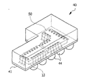
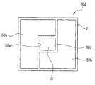
図4は、本発明の実施形態におけるマルチチップパッケージ40を示す図で、従来の矩形の第1集積回路チップ12と本発明において変形された外側部を有する第2集積回路チップ50とが基板41に実装される構造を有する。基板41は、集積回路チップと回路基板及びソケットとその他フィクスチャーとを繋ぐためにソルダボール44のような外部接続構造を有する。
FIG. 4 is a diagram showing a
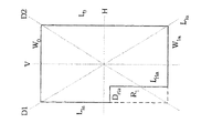
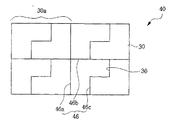
図5に示すように、本発明における集積回路チップは、端部に一つ以上の凹部R1...Rnが形成され従来の集積回路チップとは相違する。凹部は外周面と平行に形成された端部RD1、RL1を有する。少なくとも一つの凹部は少なくとも一つの端部に形成され、隣接した凹部同士に交差してL字に具現され得る。集積回路チップ、凹部の配置及び方向は、対角線軸D1、D2と平行線軸V、Hを基準にしてなっており、一つ以上の軸を基準にして対称に配置される。 As shown in FIG. 5, the integrated circuit chip according to the present invention has one or more recesses R1. . . Rn is formed and is different from the conventional integrated circuit chip. The recess has end portions RD1 and RL1 formed in parallel with the outer peripheral surface. The at least one recess may be formed in at least one end, and may be implemented in an L shape by intersecting adjacent recesses. The arrangement and direction of the integrated circuit chip and the recess are based on the diagonal axes D1 and D2 and the parallel line axes V and H, and are arranged symmetrically with respect to one or more axes.
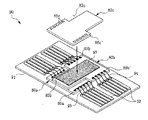
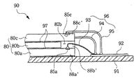
図6及び図7に示すように、マルチチップ積層パッケージ90は、チップ実装領域周囲で複数のリードまたは伝導性パターンが形成される基板91を備える。複数の集積回路チップ80a、80b、80cは、基板のチップ実装領域に順次に積層される。各々の集積回路チップには一端の両側に一対の凹部82a、82b、82cが形成されている。集積回路チップの他端の両側は元来の幅を維持しながら複数のボンドパッド88a、88b、88cが形成されており、集積回路チップとリード92は、ボンディングワイヤ93、94、95と連結する。集積回路チップ80a、80b、80cは、接着層97を用いて基板に取り付けられるが、このとき、上部に取り付けられる集積回路チップ80b、80cを下部チップに対して180°回転させて実装することができる。このような方法で、上部チップの凹部及び下部チップの周辺領域が連続して配列されると、集積回路チップの厚さよりも大きい開口部が形成され、ボンディングワイヤ93を下部チップのボンドパッド85aに取り付けることができる。
As shown in FIGS. 6 and 7, the multi-chip stacked
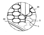
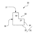
図8に示すように、互いに直交する側面36、37を有する集積回路チップ30に一つの凹部32を形成すると、凹部端部36’’、37’’の長さに減少された少なくとも二つの外周面36’、37’が生まれる。凹部の大きさ及び配置に応じて集積回路チップ30の形態が変わるが、凹部が角を取り囲む場合、集積回路チップ30はL字に具現され、図8に、図示していないが、凹部が集積回路チップの一面に形成される場合、C字に具現される。
As shown in FIG. 8, when one
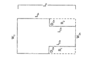
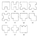
一つ以上の凹部が形成される場合、図9(a)〜(k)に示すように、集積回路チップに多様な外周面が具現されている。図5に示すように、凹部の大きさ及び配置に応じて集積回路チップの外周面は、一つ以上の対角線軸及び/または平行線軸を基準にして対称をなす。例えば、(a)の外周面は、軸(V)を基準にして対称状で、(b)の外周面は、二本の軸(V、H)を基準にして対称状で、(e)の外周面は、四本の軸(D1、D2、V、H)を基準にして対称をなす。 When one or more recesses are formed, various outer peripheral surfaces are embodied in the integrated circuit chip as shown in FIGS. As shown in FIG. 5, according to the size and arrangement of the recesses, the outer peripheral surface of the integrated circuit chip is symmetric with respect to one or more diagonal axes and / or parallel axis. For example, the outer peripheral surface of (a) is symmetrical with respect to the axis (V), and the outer peripheral surface of (b) is symmetrical with respect to the two axes (V, H). The outer peripheral surface is symmetrical with respect to four axes (D1, D2, V, H).
図10に示すように、段差を有する複数の集積回路チップら30が半導体ウエハに反復パターンで配列される。すなわち、集積回路チップは、同一方向に配列された後、切断線26a、26b、26cに沿ってスクライビング、特にレーザースクライビングにより分離される。切断された部位31は除去され集積回路チップ30に凹部が形成されることになる。切断された部位31は、個別半導体素子に含まれず、一般にこの部分はスクラップと呼ばれる。
As shown in FIG. 10, a plurality of
図11に示すように、凹部を有する集積回路チップが二以上集まって矩形の一つのユニット30aをなす。このような配置は、半導体ウエハ表面に反復的に行われることができ、切断線80a、80b、80cに沿って個別集積回路チップに分離するとスクラップを減少させることができることから素子当たり必要とする製造費用をも低減できる。
As shown in FIG. 11, two or more integrated circuit chips having recesses are gathered to form a
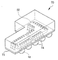
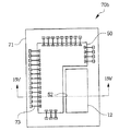
図12は、本発明の実施形態におけるマルチチップパッケージ70を示す図で、従来の矩形第1集積回路チップ12と本発明の外周面を有する第2集積回路チップ50とが基板71に水平に実装される構造である。基板71は、集積回路チップと回路基板及びソケットとフィクスチャーを繋ぐためにソルダボール74のような外部連結構造を含む。
FIG. 12 is a diagram showing a
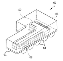
図13は、本発明の実施形態におけるシングルチップパッケージ60を示す図で、変形された外周面を有する一つの集積回路チップ50を備える構造である。集積回路チップ50は、基板61に実装され、基板61は、集積回路チップと回路基板及びソケットとフィクスチャーを繋ぐソルダボール64のような外部接続構造を有する。図12及び図13に示すように、具現された半導体素子パッケージもやはりチップの構造に対応する外周面を有するので外周面が矩形ではない。
FIG. 13 is a view showing a
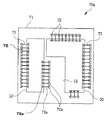
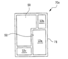
図14に示すように、本発明は、集積回路チップに凹部を形成して外周面を変形させるだけではなく、隣接した集積回路チップの配置及び連結手段を考慮してボンドパッドの配列を変えることができる。図14に示すように、マルチチップパッケージ70は、矩形集積回路チップ12と変形集積回路チップ50とが水平に実装される構造を有する。しかし、集積回路チップ12、50及び基板71のボンドパッド72、72a、75、75aが端部及び/または縦軸に沿って一律的に配列されるのではなく、従来と異なって若干非対称的に配列されている。特に、集積回路チップ50には凹部の端部52に沿ってボンドパッドが形成されておらず、矩形集積回路チップ12には集積回路チップ50の凹部で作られた空間に基板71の外側と隣接していない端部の一部に内部ボンドパッド75aが形成されている。集積回路チップのボンドパッド及び基板のボンドパッドは、ボンディングワイヤ73、73aと連結される。
As shown in FIG. 14, the present invention not only forms the recesses in the integrated circuit chip to deform the outer peripheral surface, but also changes the arrangement of the bond pads in consideration of the arrangement and connection means of adjacent integrated circuit chips. Can do. As shown in FIG. 14, the
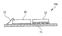
図15A及び図15Bに示すように、本発明のさらに他の実施形態におけるマルチチップパッケージ70bで、凹部の端部52に沿って集積回路チップのボンドパッドが形成されない構造を有する。
As shown in FIGS. 15A and 15B, a
図15Bは、図15Aの15b’―15b’線に沿って切断された断面図で、集積回路チップ12が、基板にフリップチップボンディングされ集積回路チップの活性面に形成されているボンドパッド及び基板のボンドパッドが半田ボールや半田バンプのような伝導性構造により直接連結された構造を有する。従って、ボンディングワイヤ73を用いる必要がない。
FIG. 15B is a cross-sectional view taken along the line 15b′-15b ′ of FIG. 15A, in which the
図16は、本発明のさらに他の実施形態に関し、マルチチップパッケージ炉及び集積回路チップ12a、12b、12c、50が基板71にフリップチップボンディングされている構造を示す。これにより、ボンディングワイヤが不要となり、基板に対する集積回路チップの実装密度が向上し、かつ取り付けが簡単に行える。また、形態の異なる集積回路チップを基板表面に完全な形態で配置できるため、実装密度を高めることができる。
FIG. 16 shows a structure in which a multi-chip package furnace and
図17は、本発明のさらに他の実施形態に関し、マルチチップパッケージ炉及び集積回路チップ12、50a、50bの凹部の端部52a、52b間で形成された内部空間に集積回路チップ12が配置されている構造を示す。各々の集積回路チップは、基板にフリップチップボンディングされるのでワイヤボンディングが不要で、これにより基板に対する集積回路チップの実装密度が向上し、かつ取り付けが簡単に行える。
FIG. 17 relates to still another embodiment of the present invention, in which the
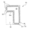
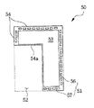
図18に示すように、本発明の実施形態における集積回路チップ50は、チップ最端部57、56、角部51、及びボンドパッド54、54aが一定に配列された凹部端部54aを含む構造である。図19は、集積回路チップ50のさらに他の実施形態を示すもので、ボンドパッドがチップ端部のみに形成されており凹部端部54aには形成されていない。例えば、図17のマルチチップ構造のように、凹部間に形成された空間により他の集積回路チップを配置させることができ、そうした構造に有用である。
As shown in FIG. 18, the
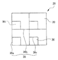
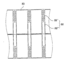
図20A及び図20Bは、ボンドパッドが形成された周辺領域88’と凹部領域88’’とを含む外周面88を有する集積回路チップ80が複数配置された構造を示している。図20Bに示すように、基板上での集積回路チップの方向を変えることにより開放領域やスクラップを減少させながら実装密度を高めることができる。しかし、集積回路チップで具現され得ない半導体ウエハ部分はそのまま置いたほうが良い。つまり、当該部分は、新しい製造過程や生産ラインまたは新しい装置を用いる際パラメータ及び機能テストを行うテストプラグ構造を作るのに必要だからである。このようなテスト構造により、キャパシタ、レジスタ、トランジスタ及び配置構造等が分析できることから、重要な機能的構成の品質や効果的な大きさを理解することができる。
20A and 20B show a structure in which a plurality of
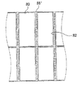
図21は、図20A及び図20Bの集積回路チップから分離段階を経て得られた個別集積回路チップ80を示す図である。図20A及び図20Bに示すように、集積回路チップ80の第1段の両側に二つの凹部領域82が形成されており、第2段の両側に表面86を有する周辺領域88が形成されている。周辺領域88及び凹部領域82は、素子が適切に機能するための必要なメモリ、論理及び/または入出力回路を含む内部機能領域、すなわちセル領域83を取り囲む形状である。チップの周辺領域は、隅部84、81となる左右側上端領域89、87を含む。
FIG. 21 is a diagram showing an individual
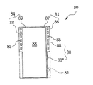
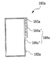
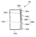
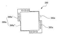
図22に示すように、本発明のさらに他の実施形態の集積回路チップ180aによると、ボンドパッド185aが形成された周辺領域188a’及び周辺領域と一緒にチップの一側面188aを形成する凹部領域188a’’を含む一つの凹部182aを有する。図23に示すように、本発明の実施形態によるマルチチップパッケージ190は、図22の第1集積回路チップ180a上に第2集積回路チップ180bが積層されている構造を有する。第2集積回路チップ180bは第1集積回路チップと反対方向の周辺領域188b’及び凹部端部188b’’を含む。すなわち、第1チップ180a上に第2チップ180bが積層されるとき、またはその反対の場合、上部チップの凹部領域が下部チップのボンドパッド185bを露出させることによって、チップと基板との連結の際一列に形成されたボンドパッド185a、185bを提供する。
As shown in FIG. 22, according to an
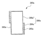
図24に示すように、本発明のさらに他の実施形態における集積回路チップ280aは、チップ両側に形成された二つの凹部282a、288aを有し、一方の凹部288aは、ボンドパッドが形成された周辺領域288a’と凹部領域299a’’とを含む。図25に示すように、本発明の実施形態におけるマルチチップパッケージ290は、図24の第1集積回路チップ280a上に第2集積回路チップ280bが積層された構造を有する。第2集積回路チップ280bは、第1集積回路チップ280aと反対方向の周辺領域288b’と凹部領域288b’’とを含む。すなわち、第1チップ280a上に第2チップ280bが積層される時、またはその反対の場合、上部チップの凹部領域が下部チップのボンドパッド286bを露出させる。これにより、チップと基板との連結際両列に形成されたボンドパッド285a、285bを提供する。
As shown in FIG. 24, an
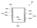
図26に示すように、本発明のさらに他の実施形態における集積回路チップ290は、チップ対角線角に形成された一対の凹部382a、388aを有し、一方の凹部388aは、ボンドパッドが形成された周辺領域388a’と凹部領域388a’’とを含む。図27に示すように、本発明の実施形態によるマルチチップパッケージ390は、図26の第1集積回路チップ290上に第2集積回路チップ290を90°回転させて積層した構造を有する。図27に示すように、第2チップは、第1チップと反対方向の周辺領域388b’と凹部領域388b’’とを含む。これにより、第1チップ上に第2チップが積層される場合またはその反対の場合、上部チップの凹部領域が下部チップのボンドパッド385bを露出することによって、チップと基板との連結際端部に沿って形成されるボンドパッド385a、385bを提供する。
As shown in FIG. 26, an
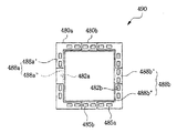
図28に示すように、本発明のもう一つの実施形態における集積回路チップ480aは、チップ端部の中間に形成された凹部482aを有し、一つの凹部488a’’は、ボンドパッド485aが形成された周辺領域488a’と隣接周辺領域間に形成された凹部領域488a’’とを含む。図29に示すように、本発明の実施形態によるマルチチップパッケージ490は、図28の第1集積回路チップ480aと、上記第1集積回路チップ480aと相互補完的形態の凹部488aを含む第2集積回路チップ480bが積層される構造を有する。すなわち、第1チップ上に第2チップが積層されると、上部チップの凹部領域が下部チップのボンドパッド485bを露出することになる。これにより、チップと基板との連結際端部に沿って形成されたボンドパッド485a、485bを提供する。
As shown in FIG. 28, an
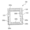
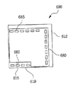
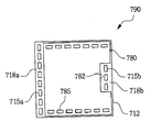
図30乃至図32に示すように、大きさと形態の異なる多様な外周面を有する集積回路チップを用いてチップスタック構造590、690、790を具現することにより、下部チップのボンドパッドを、上部チップの大きさと位置に応じて露出することができ、かつ上部チップの凹部に対応して配置することができる。よって、下部チップのボンドパッドがスペーサを追加したり背面をエッチングしたりするなどの追加工程を加えず露出することができる。
30 to 32, the
本発明の実施形態による集積回路チップは、論理及び/またはメモリ回路が形成されたセル領域、及び入出力回路及び/または入出力パッドが形成された一つ以上の周辺領域を含む構造を有する。集積回路チップのセル領域及び/または周辺領域に隣接した凹部が形成される。本発明の実施形態による集積回路チップ及びチップスタック構造は、ワイヤボンディング及び/またはフリップチップボンディングのような連結方法を用いて一つ以上の基板に連結できる。そして、エポキシモルディング化合物のような樹脂密封材で密封し、集積回路チップ、ワイヤボンディング及びインナーリードの汚染、副食または機械的損傷から保護することができる。 An integrated circuit chip according to an embodiment of the present invention has a structure including a cell region in which logic and / or memory circuits are formed, and one or more peripheral regions in which input / output circuits and / or input / output pads are formed. A recess is formed adjacent to the cell region and / or the peripheral region of the integrated circuit chip. Integrated circuit chips and chip stack structures according to embodiments of the present invention can be connected to one or more substrates using connection methods such as wire bonding and / or flip chip bonding. Then, it can be sealed with a resin sealing material such as an epoxy molding compound to protect the integrated circuit chip, wire bonding, and inner leads from contamination, side effects, or mechanical damage.
本明細書に開示された連結方法である、ワイヤボンディング、フリップチップボンディング及び/またはTAB方法だけでなく、多様な方法が使用可能であり、基板として、リードフレーム、印刷回路基板、フレキシブル回路基板またはセラミック基板以外にも多様な基板が使用可能である。 In addition to wire bonding, flip chip bonding and / or TAB methods, which are the connection methods disclosed in the present specification, various methods can be used. As a substrate, a lead frame, a printed circuit board, a flexible circuit board, Various substrates other than the ceramic substrate can be used.
以上、本発明の実施例によって多様な外周面とボンドパッド構造を有する集積回路チップは、基板及び/またはパッケージと一緒に用いることができる。また、多様な要素等と適合できるので捨てられる表面領域が低減し、基板または第2回路基板に対する実装密度を向上させることができる。マルチチップパッケージに対する素子水準、またはパッケージが実装されるマザーボードやモジュールボードのような上位水準において実装密度を向上させることができる。さらに、基板水準においてパッケージの実装密度を向上させることによって基板の大きさを小さくすることができる。 As described above, the integrated circuit chip having various outer peripheral surfaces and bond pad structures according to the embodiment of the present invention can be used together with the substrate and / or the package. Further, since it can be adapted to various elements and the like, the surface area to be discarded can be reduced, and the mounting density on the substrate or the second circuit substrate can be improved. The mounting density can be improved at the element level for the multi-chip package or at a higher level such as a mother board or module board on which the package is mounted. Furthermore, the size of the substrate can be reduced by improving the packaging density of the package at the substrate level.
なお、本明細書と図面に開示された本発明の実施形態は理解を助けるための特定例を提示したに過ぎず、本発明の範囲を限定するものではない。ここに開示された実施形態の他にも本発明の技術的思想に基づき他の変形例が実施可能であることは本発明が属する技術分野における通常の知識を有する者に自明である It should be noted that the embodiments of the present invention disclosed in this specification and the drawings are merely provided as specific examples for helping understanding, and do not limit the scope of the present invention. It will be apparent to those skilled in the art to which the present invention pertains that other variations can be implemented based on the technical concept of the present invention in addition to the embodiments disclosed herein.
40 マルチチップパッケージ
41 基板
82a,82b,82c 凹部
182a 凹部
282a,288a 凹部
382a,388a 凹部
482a,488a 凹部
40
Claims (34)
最大幅W0と、
最大長さL0と、
第1凹部
とを有し、
前記W0において第1凹部深さDrla減少されて第1短軸幅Wlaが形成され、前記L0において第1凹部長さLrla減少されて第1短軸長さLlaが形成されることを特徴とする半導体ダイ。 In a semiconductor die having a deformed rectangular perimeter,
Maximum width W 0 ,
Maximum length L 0 ,
A first recess,
In W 0 , the first recess depth D rla is reduced to form a first minor axis width W la , and in L 0 , the first recess length L rla is reduced to form a first minor axis length L la. A semiconductor die characterized by that.
前記W0において第2凹部深さDRr2a減少されて第2幅W2aが形成され、前記L0において第2凹部長さLr2a減少されて第2長さL2aが形成されることを特徴とする請求項1に記載の半導体ダイ。 A second recess,
The second recess depth DR r2a is reduced at W 0 to form a second width W 2a , and the second recess length L r2a is reduced at L 0 to form a second length L 2a. A semiconductor die according to claim 1.
前記W0においてN番目凹部深さDrNaに減少されて第N幅WNaが形成され、前記L0がN番目凹部長さLrNaに減少されて第N長さLNaが形成されることを特徴とする請求項2に記載の半導体ダイ。 An even number of N recesses;
In the W 0 , the Nth width W Na is formed by reducing the Nth recess depth D rNa , and the L 0 is reduced by the Nth recess length L rNa to form the Nth length L Na. The semiconductor die according to claim 2.
前記第2凹部は、前記半導体ダイの第1角と異なる第2角を取り囲むことを特徴とする請求項2に記載の半導体ダイ。 The first recess surrounds a first corner of the semiconductor die;
The semiconductor die according to claim 2, wherein the second recess surrounds a second corner different from the first corner of the semiconductor die.
前記ウエハにおいて個別ダイを分離する段階と
を有することを特徴とする半導体素子製造方法。 Forming a plurality of dies having recesses on the outer periphery on a semiconductor wafer;
Separating the individual dies in the wafer.
前記脆弱な部分に沿って隣接するダイから個別ダイを分離する段階と、
を有することを特徴とする請求項15に記載の半導体素子製造方法。 The separating step includes laser scribing the outer peripheral surface of the die to form a fragile portion on the wafer;
Separating individual dies from adjacent dies along the fragile portion;
The method of manufacturing a semiconductor device according to claim 15, comprising:
前記活性面の反対面においてウエハの下部を除去して上下部がウエハの元来の厚さと少なくとも同じくする段階と、
ダイ間の切断線に沿って前記ウエハの残り部分を除去する段階と、
を有することを特徴とする請求項15に記載の半導体素子製造方法。 The separating step includes removing an upper portion of the wafer adjacent to the recess outside the outer peripheral surface of the die to form an opening in the active surface of the wafer;
Removing the lower portion of the wafer on the opposite side of the active surface, so that the upper and lower portions are at least the same as the original thickness of the wafer;
Removing the remaining portion of the wafer along a cutting line between dies;
The method of manufacturing a semiconductor device according to claim 15, comprising:
外周面に凹部を有する第1半導体ダイと、
を備える半導体素子パッケージにおいて、
前記接触部が凹部を介して露出するように前記基板に第1半導体ダイを実装することを特徴とする半導体素子パッケージ。 A substrate having a contact portion;
A first semiconductor die having a recess on an outer peripheral surface;
In a semiconductor device package comprising:
A semiconductor device package, wherein a first semiconductor die is mounted on the substrate such that the contact portion is exposed through a recess.
複数のボンドパッドは、前記第1半導体ダイの活性面に形成することを特徴とする請求項22に記載の半導体素子パッケージ。 The substrate is a lower semiconductor die, and the contact portion comprises at least one bond pad;
The semiconductor device package of claim 22, wherein a plurality of bond pads are formed on an active surface of the first semiconductor die.
外周面に凹部が形成された第1半導体ダイと、
を備える半導体素子パッケージにおいて、
前記接触部が凹部を介して露出するように前記基板に第1半導体ダイが実装されることを特徴とする請求項22に記載の半導体素子パッケージ。 A substrate having a contact surface;
A first semiconductor die having a recess formed on the outer peripheral surface;
In a semiconductor device package comprising:
23. The semiconductor device package of claim 22, wherein a first semiconductor die is mounted on the substrate such that the contact portion is exposed through a recess.
前記基板に複数の第1ボンドパッドを有する第1半導体ダイを実装する段階と、
外周面に第1凹部が形成された第2半導体ダイを形成する段階と、
前記複数の第1ボンドパッドが前記第1凹部を介して露出するように前記第1半導体ダイ上に前記第2半導体ダイを実装する段階と、
を有することを特徴とする半導体素子パッケージ製造方法。 Preparing a substrate;
Mounting a first semiconductor die having a plurality of first bond pads on the substrate;
Forming a second semiconductor die having a first recess formed on an outer peripheral surface;
Mounting the second semiconductor die on the first semiconductor die such that the plurality of first bond pads are exposed through the first recess;
A method of manufacturing a semiconductor device package, comprising:
前記第2半導体素子の活性面に形成されている複数の第2ボンドパッドが、前記第2凹部を介して露出するように前記第2半導体ダイ上に前記第3半導体ダイを実装する段階と、
をさらに有することを特徴とする半導体素子パッケージ製造方法。 Forming a third semiconductor element in which the second recess is deformed on the deformed rectangular outer peripheral surface;
Mounting the third semiconductor die on the second semiconductor die such that a plurality of second bond pads formed on the active surface of the second semiconductor element are exposed through the second recess;
A method of manufacturing a semiconductor device package, further comprising:
外周面に凹部が形成されており、基板に実装される第1半導体ダイと、
前記凹部内に位置するように前記第1半導体ダイと水平に実装され第2半導体ダイと、
を備えることを特徴とする半導体素子パッケージ。 In a semiconductor device package comprising at least two semiconductor dies,
A recess formed in the outer peripheral surface, and a first semiconductor die mounted on the substrate;
A second semiconductor die mounted horizontally with the first semiconductor die so as to be located in the recess;
A semiconductor device package comprising:
33. The semiconductor device of claim 32, wherein the second semiconductor die is completely located in the recess.
Applications Claiming Priority (2)
| Application Number | Priority Date | Filing Date | Title |
|---|---|---|---|
| KR1020040022666A KR100627006B1 (en) | 2004-04-01 | 2004-04-01 | Indent chips, semiconductor packages and multi-chip packages using the same |
| KR2004-022666 | 2004-04-01 |
Publications (2)
| Publication Number | Publication Date |
|---|---|
| JP2005294842A true JP2005294842A (en) | 2005-10-20 |
| JP4832782B2 JP4832782B2 (en) | 2011-12-07 |
Family
ID=34985361
Family Applications (1)
| Application Number | Title | Priority Date | Filing Date |
|---|---|---|---|
| JP2005103706A Expired - Fee Related JP4832782B2 (en) | 2004-04-01 | 2005-03-31 | Semiconductor package having step type die and method of manufacturing the same |
Country Status (4)
| Country | Link |
|---|---|
| US (1) | US7485955B2 (en) |
| JP (1) | JP4832782B2 (en) |
| KR (1) | KR100627006B1 (en) |
| DE (1) | DE102005016439B4 (en) |
Cited By (8)
| Publication number | Priority date | Publication date | Assignee | Title |
|---|---|---|---|---|
| JP2011146718A (en) * | 2010-01-18 | 2011-07-28 | Semiconductor Components Industries Llc | Method of forming semiconductor die |
| JP2011228711A (en) * | 2010-04-19 | 2011-11-10 | Tokyo Electron Ltd | Method for separation and conveyance of semiconductor integrated circuit chip |
| JP2014017413A (en) * | 2012-07-10 | 2014-01-30 | Denso Corp | Semiconductor device and manufacturing method of the same |
| JP2014072239A (en) * | 2012-09-27 | 2014-04-21 | Rohm Co Ltd | Chip component |
| US9165833B2 (en) | 2010-01-18 | 2015-10-20 | Semiconductor Components Industries, Llc | Method of forming a semiconductor die |
| US9275957B2 (en) | 2010-01-18 | 2016-03-01 | Semiconductor Components Industries, Llc | EM protected semiconductor die |
| JP2023125523A (en) * | 2022-02-28 | 2023-09-07 | 三菱電機株式会社 | Semiconductor device |
| JP2023173553A (en) * | 2022-05-26 | 2023-12-07 | 浜松ホトニクス株式会社 | Wafer and wafer processing method |
Families Citing this family (17)
| Publication number | Priority date | Publication date | Assignee | Title |
|---|---|---|---|---|
| US6551857B2 (en) | 1997-04-04 | 2003-04-22 | Elm Technology Corporation | Three dimensional structure integrated circuits |
| US7579681B2 (en) * | 2002-06-11 | 2009-08-25 | Micron Technology, Inc. | Super high density module with integrated wafer level packages |
| AU2003255254A1 (en) | 2002-08-08 | 2004-02-25 | Glenn J. Leedy | Vertical system integration |
| KR100627006B1 (en) * | 2004-04-01 | 2006-09-25 | 삼성전자주식회사 | Indent chips, semiconductor packages and multi-chip packages using the same |
| US7545031B2 (en) * | 2005-04-11 | 2009-06-09 | Stats Chippac Ltd. | Multipackage module having stacked packages with asymmetrically arranged die and molding |
| KR101539402B1 (en) * | 2008-10-23 | 2015-07-27 | 삼성전자주식회사 | Semiconductor package |
| FR2940521B1 (en) * | 2008-12-19 | 2011-11-11 | 3D Plus | COLLECTIVE MANUFACTURING METHOD OF ELECTRONIC MODULES FOR SURFACE MOUNTING |
| US20110233718A1 (en) * | 2010-03-25 | 2011-09-29 | Qualcomm Incorporated | Heterogeneous Technology Integration |
| JP5995563B2 (en) * | 2012-07-11 | 2016-09-21 | 株式会社ディスコ | Optical device processing method |
| KR101999114B1 (en) * | 2013-06-03 | 2019-07-11 | 에스케이하이닉스 주식회사 | semiconductor package |
| TWI564997B (en) * | 2015-06-12 | 2017-01-01 | 萬國半導體股份有限公司 | Power semiconductor device and the fabricating method thereof |
| US10037946B2 (en) | 2016-02-05 | 2018-07-31 | Dyi-chung Hu | Package structure having embedded bonding film and manufacturing method thereof |
| US9806044B2 (en) * | 2016-02-05 | 2017-10-31 | Dyi-chung Hu | Bonding film for signal communication between central chip and peripheral chips and fabricating method thereof |
| KR102358343B1 (en) | 2017-08-09 | 2022-02-07 | 삼성전자주식회사 | Semiconductor package |
| KR102378837B1 (en) * | 2018-08-24 | 2022-03-24 | 삼성전자주식회사 | Semiconductor device and semiconductor package comprising the same |
| US20240006397A1 (en) * | 2022-06-30 | 2024-01-04 | Prilit Optronics, Inc. | Display panel |
| TWI841184B (en) * | 2023-01-09 | 2024-05-01 | 福懋科技股份有限公司 | Semiconductor package and manufacturing method thereof |
Citations (2)
| Publication number | Priority date | Publication date | Assignee | Title |
|---|---|---|---|---|
| JPH05267449A (en) * | 1992-03-19 | 1993-10-15 | Mitsubishi Electric Corp | Semiconductor device and manufacturing method thereof |
| JPH11224864A (en) * | 1998-02-06 | 1999-08-17 | Mitsubishi Electric Corp | Semiconductor wafer chip separation method |
Family Cites Families (17)
| Publication number | Priority date | Publication date | Assignee | Title |
|---|---|---|---|---|
| US3538400A (en) | 1967-07-31 | 1970-11-03 | Nippon Electric Co | Semiconductor gunn effect switching element |
| US3816906A (en) | 1969-06-20 | 1974-06-18 | Siemens Ag | Method of dividing mg-al spinel substrate wafers coated with semiconductor material and provided with semiconductor components |
| JPS6193613A (en) | 1984-10-15 | 1986-05-12 | Nec Corp | Semiconductor integrated circuit device |
| US5323060A (en) | 1993-06-02 | 1994-06-21 | Micron Semiconductor, Inc. | Multichip module having a stacked chip arrangement |
| JP3007023B2 (en) | 1995-05-30 | 2000-02-07 | シャープ株式会社 | Semiconductor integrated circuit and method of manufacturing the same |
| KR19980067184A (en) | 1997-01-31 | 1998-10-15 | 김광호 | Inline device with simultaneous wafer cutting and die bonding |
| KR19980084225A (en) | 1997-05-22 | 1998-12-05 | 윤종용 | Semiconductor Wafer Cutting Machine |
| JP3670853B2 (en) | 1998-07-30 | 2005-07-13 | 三洋電機株式会社 | Semiconductor device |
| JP3643705B2 (en) | 1998-07-31 | 2005-04-27 | 三洋電機株式会社 | Semiconductor device and manufacturing method thereof |
| JP2000306865A (en) | 1999-02-17 | 2000-11-02 | Toshiba Electronic Engineering Corp | Wafer-cutting method and apparatus |
| US6605875B2 (en) | 1999-12-30 | 2003-08-12 | Intel Corporation | Integrated circuit die having bond pads near adjacent sides to allow stacking of dice without regard to dice size |
| JP3832170B2 (en) | 2000-01-06 | 2006-10-11 | セイコーエプソン株式会社 | Multi-bare chip assembly |
| US6359340B1 (en) | 2000-07-28 | 2002-03-19 | Advanced Semiconductor Engineering, Inc. | Multichip module having a stacked chip arrangement |
| KR100401020B1 (en) | 2001-03-09 | 2003-10-08 | 앰코 테크놀로지 코리아 주식회사 | Stacking structure of semiconductor chip and semiconductor package using it |
| KR100407472B1 (en) | 2001-06-29 | 2003-11-28 | 삼성전자주식회사 | Chip-Stacked Package Device Having Upper Chip Provided With Corner Trenchs And Method For Manufacturing the Same |
| KR20030075860A (en) | 2002-03-21 | 2003-09-26 | 삼성전자주식회사 | Structure for stacking semiconductor chip and stacking method |
| KR100627006B1 (en) * | 2004-04-01 | 2006-09-25 | 삼성전자주식회사 | Indent chips, semiconductor packages and multi-chip packages using the same |
-
2004
- 2004-04-01 KR KR1020040022666A patent/KR100627006B1/en not_active Expired - Fee Related
-
2005
- 2005-03-11 US US11/077,235 patent/US7485955B2/en not_active Expired - Lifetime
- 2005-03-31 JP JP2005103706A patent/JP4832782B2/en not_active Expired - Fee Related
- 2005-04-01 DE DE102005016439A patent/DE102005016439B4/en not_active Expired - Lifetime
Patent Citations (2)
| Publication number | Priority date | Publication date | Assignee | Title |
|---|---|---|---|---|
| JPH05267449A (en) * | 1992-03-19 | 1993-10-15 | Mitsubishi Electric Corp | Semiconductor device and manufacturing method thereof |
| JPH11224864A (en) * | 1998-02-06 | 1999-08-17 | Mitsubishi Electric Corp | Semiconductor wafer chip separation method |
Cited By (11)
| Publication number | Priority date | Publication date | Assignee | Title |
|---|---|---|---|---|
| JP2011146718A (en) * | 2010-01-18 | 2011-07-28 | Semiconductor Components Industries Llc | Method of forming semiconductor die |
| US9165833B2 (en) | 2010-01-18 | 2015-10-20 | Semiconductor Components Industries, Llc | Method of forming a semiconductor die |
| US9275957B2 (en) | 2010-01-18 | 2016-03-01 | Semiconductor Components Industries, Llc | EM protected semiconductor die |
| US9299664B2 (en) | 2010-01-18 | 2016-03-29 | Semiconductor Components Industries, Llc | Method of forming an EM protected semiconductor die |
| US9437493B2 (en) | 2010-01-18 | 2016-09-06 | Semiconductor Components Industries, Llc | Method of forming a semiconductor die |
| JP2011228711A (en) * | 2010-04-19 | 2011-11-10 | Tokyo Electron Ltd | Method for separation and conveyance of semiconductor integrated circuit chip |
| JP2014017413A (en) * | 2012-07-10 | 2014-01-30 | Denso Corp | Semiconductor device and manufacturing method of the same |
| JP2014072239A (en) * | 2012-09-27 | 2014-04-21 | Rohm Co Ltd | Chip component |
| JP2023125523A (en) * | 2022-02-28 | 2023-09-07 | 三菱電機株式会社 | Semiconductor device |
| JP7729235B2 (en) | 2022-02-28 | 2025-08-26 | 三菱電機株式会社 | Semiconductor Devices |
| JP2023173553A (en) * | 2022-05-26 | 2023-12-07 | 浜松ホトニクス株式会社 | Wafer and wafer processing method |
Also Published As
| Publication number | Publication date |
|---|---|
| KR100627006B1 (en) | 2006-09-25 |
| JP4832782B2 (en) | 2011-12-07 |
| DE102005016439A1 (en) | 2005-10-20 |
| US20050205975A1 (en) | 2005-09-22 |
| DE102005016439B4 (en) | 2011-07-28 |
| US7485955B2 (en) | 2009-02-03 |
| KR20050097586A (en) | 2005-10-10 |
Similar Documents
| Publication | Publication Date | Title |
|---|---|---|
| JP4832782B2 (en) | Semiconductor package having step type die and method of manufacturing the same | |
| KR100594229B1 (en) | Semiconductor package and manufacturing method | |
| WO2006044804A2 (en) | Multi chip leadframe package | |
| KR20080013305A (en) | Multi-chip package in which a plurality of semiconductor chips of different sizes are stacked and manufacturing method thereof | |
| JP2003078106A (en) | Chip stacked package element and method of manufacturing the same | |
| TW201737446A (en) | Semiconductor package with multiple coplanar interposers | |
| TWI446461B (en) | Integrated circuit package system with external interconnect array | |
| CN112670191A (en) | Semiconductor packaging method, semiconductor packaging structure and packaging body | |
| CN101447441A (en) | Integrated circuit package system including die having relieved active region | |
| US20090203171A1 (en) | Semiconductor device fabricating method | |
| KR102739235B1 (en) | Semiconductor package | |
| US20170179101A1 (en) | Bridge structure for embedding semiconductor die | |
| CN100448003C (en) | Semiconductor device | |
| US9462694B2 (en) | Spacer layer for embedding semiconductor die | |
| JP4497304B2 (en) | Semiconductor device and manufacturing method thereof | |
| JP2002100707A (en) | Semiconductor device and method of manufacturing the same | |
| US7445944B2 (en) | Packaging substrate and manufacturing method thereof | |
| TW202230710A (en) | Semiconductor package and method of manufacture | |
| TWI883655B (en) | Semiconductor device and method for manufacturing semiconductor device | |
| US20260068740A1 (en) | Semiconductor chip and semiconductor package including the same | |
| CN101609818A (en) | Semiconductor packaging device, semiconductor packaging structure and manufacturing method thereof | |
| CN100378977C (en) | Semiconductor device without chip carrier and manufacturing method thereof | |
| KR100681264B1 (en) | Electronic device package and manufacturing method thereof | |
| TW201236115A (en) | Method for manufacturing semiconductor chips, mounting method and semiconductor chip for vertical mounting onto circuit substrates | |
| KR20240108618A (en) | Semiconductor package and method of manufacturing the semiconductor package |
Legal Events
| Date | Code | Title | Description |
|---|---|---|---|
| A621 | Written request for application examination |
Free format text: JAPANESE INTERMEDIATE CODE: A621 Effective date: 20071107 |
|
| A977 | Report on retrieval |
Free format text: JAPANESE INTERMEDIATE CODE: A971007 Effective date: 20100603 |
|
| A131 | Notification of reasons for refusal |
Free format text: JAPANESE INTERMEDIATE CODE: A131 Effective date: 20100608 |
|
| A521 | Request for written amendment filed |
Free format text: JAPANESE INTERMEDIATE CODE: A523 Effective date: 20100907 |
|
| A02 | Decision of refusal |
Free format text: JAPANESE INTERMEDIATE CODE: A02 Effective date: 20110322 |
|
| A521 | Request for written amendment filed |
Free format text: JAPANESE INTERMEDIATE CODE: A523 Effective date: 20110720 |
|
| A911 | Transfer to examiner for re-examination before appeal (zenchi) |
Free format text: JAPANESE INTERMEDIATE CODE: A911 Effective date: 20110801 |
|
| TRDD | Decision of grant or rejection written | ||
| A01 | Written decision to grant a patent or to grant a registration (utility model) |
Free format text: JAPANESE INTERMEDIATE CODE: A01 Effective date: 20110823 |
|
| A01 | Written decision to grant a patent or to grant a registration (utility model) |
Free format text: JAPANESE INTERMEDIATE CODE: A01 |
|
| A61 | First payment of annual fees (during grant procedure) |
Free format text: JAPANESE INTERMEDIATE CODE: A61 Effective date: 20110921 |
|
| R150 | Certificate of patent or registration of utility model |
Ref document number: 4832782 Country of ref document: JP Free format text: JAPANESE INTERMEDIATE CODE: R150 |
|
| FPAY | Renewal fee payment (event date is renewal date of database) |
Free format text: PAYMENT UNTIL: 20140930 Year of fee payment: 3 |
|
| R250 | Receipt of annual fees |
Free format text: JAPANESE INTERMEDIATE CODE: R250 |
|
| R250 | Receipt of annual fees |
Free format text: JAPANESE INTERMEDIATE CODE: R250 |
|
| R250 | Receipt of annual fees |
Free format text: JAPANESE INTERMEDIATE CODE: R250 |
|
| R250 | Receipt of annual fees |
Free format text: JAPANESE INTERMEDIATE CODE: R250 |
|
| R250 | Receipt of annual fees |
Free format text: JAPANESE INTERMEDIATE CODE: R250 |
|
| R250 | Receipt of annual fees |
Free format text: JAPANESE INTERMEDIATE CODE: R250 |
|
| R250 | Receipt of annual fees |
Free format text: JAPANESE INTERMEDIATE CODE: R250 |
|
| R250 | Receipt of annual fees |
Free format text: JAPANESE INTERMEDIATE CODE: R250 |
|
| R250 | Receipt of annual fees |
Free format text: JAPANESE INTERMEDIATE CODE: R250 |
|
| R250 | Receipt of annual fees |
Free format text: JAPANESE INTERMEDIATE CODE: R250 |
|
| LAPS | Cancellation because of no payment of annual fees |