JP2004040099A - オプトエレクトロニクス素子およびオプトエレクトロニクス素子の製造方法 - Google Patents
オプトエレクトロニクス素子およびオプトエレクトロニクス素子の製造方法 Download PDFInfo
- Publication number
- JP2004040099A JP2004040099A JP2003182480A JP2003182480A JP2004040099A JP 2004040099 A JP2004040099 A JP 2004040099A JP 2003182480 A JP2003182480 A JP 2003182480A JP 2003182480 A JP2003182480 A JP 2003182480A JP 2004040099 A JP2004040099 A JP 2004040099A
- Authority
- JP
- Japan
- Prior art keywords
- cavity
- semiconductor chip
- filling
- particles
- base casing
- Prior art date
- Legal status (The legal status is an assumption and is not a legal conclusion. Google has not performed a legal analysis and makes no representation as to the accuracy of the status listed.)
- Pending
Links
- 230000005693 optoelectronics Effects 0.000 title claims abstract description 33
- 238000004519 manufacturing process Methods 0.000 title claims abstract description 13
- 239000004065 semiconductor Substances 0.000 claims abstract description 63
- 239000000945 filler Substances 0.000 claims abstract description 10
- 239000000463 material Substances 0.000 claims description 86
- 239000002245 particle Substances 0.000 claims description 20
- 230000005855 radiation Effects 0.000 claims description 15
- 239000000126 substance Substances 0.000 claims description 15
- 239000000758 substrate Substances 0.000 claims description 11
- GWEVSGVZZGPLCZ-UHFFFAOYSA-N Titan oxide Chemical compound O=[Ti]=O GWEVSGVZZGPLCZ-UHFFFAOYSA-N 0.000 claims description 8
- 239000003822 epoxy resin Substances 0.000 claims description 8
- 229920000647 polyepoxide Polymers 0.000 claims description 8
- 230000005670 electromagnetic radiation Effects 0.000 claims description 6
- 238000000034 method Methods 0.000 claims description 6
- 238000002310 reflectometry Methods 0.000 claims description 5
- XLOMVQKBTHCTTD-UHFFFAOYSA-N Zinc monoxide Chemical compound [Zn]=O XLOMVQKBTHCTTD-UHFFFAOYSA-N 0.000 claims description 4
- TZCXTZWJZNENPQ-UHFFFAOYSA-L barium sulfate Chemical compound [Ba+2].[O-]S([O-])(=O)=O TZCXTZWJZNENPQ-UHFFFAOYSA-L 0.000 claims description 4
- 230000001965 increasing effect Effects 0.000 claims description 4
- 239000004408 titanium dioxide Substances 0.000 claims description 4
- 229920005989 resin Polymers 0.000 claims description 3
- 239000011347 resin Substances 0.000 claims description 3
- 229910002601 GaN Inorganic materials 0.000 claims description 2
- JMASRVWKEDWRBT-UHFFFAOYSA-N Gallium nitride Chemical compound [Ga]#N JMASRVWKEDWRBT-UHFFFAOYSA-N 0.000 claims description 2
- MCMNRKCIXSYSNV-UHFFFAOYSA-N ZrO2 Inorganic materials O=[Zr]=O MCMNRKCIXSYSNV-UHFFFAOYSA-N 0.000 claims description 2
- RVTZCBVAJQQJTK-UHFFFAOYSA-N oxygen(2-);zirconium(4+) Chemical compound [O-2].[O-2].[Zr+4] RVTZCBVAJQQJTK-UHFFFAOYSA-N 0.000 claims description 2
- 229910052710 silicon Inorganic materials 0.000 claims description 2
- 239000010703 silicon Substances 0.000 claims description 2
- 239000011787 zinc oxide Substances 0.000 claims description 2
- 239000007769 metal material Substances 0.000 claims 1
- 229910010413 TiO 2 Inorganic materials 0.000 description 8
- 239000000853 adhesive Substances 0.000 description 4
- 230000001070 adhesive effect Effects 0.000 description 4
- 239000004033 plastic Substances 0.000 description 3
- 239000008393 encapsulating agent Substances 0.000 description 2
- 229910052782 aluminium Inorganic materials 0.000 description 1
- XAGFODPZIPBFFR-UHFFFAOYSA-N aluminium Chemical compound [Al] XAGFODPZIPBFFR-UHFFFAOYSA-N 0.000 description 1
- 238000005266 casting Methods 0.000 description 1
- 230000001419 dependent effect Effects 0.000 description 1
- 230000002708 enhancing effect Effects 0.000 description 1
- 238000002347 injection Methods 0.000 description 1
- 239000007924 injection Substances 0.000 description 1
- 238000001746 injection moulding Methods 0.000 description 1
- 229910052751 metal Inorganic materials 0.000 description 1
- 239000002184 metal Substances 0.000 description 1
- 239000000203 mixture Substances 0.000 description 1
- 239000004417 polycarbonate Substances 0.000 description 1
- 229920000515 polycarbonate Polymers 0.000 description 1
- 230000001568 sexual effect Effects 0.000 description 1
Images

Classifications
-
- H—ELECTRICITY
- H01—ELECTRIC ELEMENTS
- H01L—SEMICONDUCTOR DEVICES NOT COVERED BY CLASS H10
- H01L33/00—Semiconductor devices with at least one potential-jump barrier or surface barrier specially adapted for light emission; Processes or apparatus specially adapted for the manufacture or treatment thereof or of parts thereof; Details thereof
- H01L33/48—Semiconductor devices with at least one potential-jump barrier or surface barrier specially adapted for light emission; Processes or apparatus specially adapted for the manufacture or treatment thereof or of parts thereof; Details thereof characterised by the semiconductor body packages
- H01L33/483—Containers
- H01L33/486—Containers adapted for surface mounting
-
- H—ELECTRICITY
- H01—ELECTRIC ELEMENTS
- H01L—SEMICONDUCTOR DEVICES NOT COVERED BY CLASS H10
- H01L31/00—Semiconductor devices sensitive to infrared radiation, light, electromagnetic radiation of shorter wavelength or corpuscular radiation and specially adapted either for the conversion of the energy of such radiation into electrical energy or for the control of electrical energy by such radiation; Processes or apparatus specially adapted for the manufacture or treatment thereof or of parts thereof; Details thereof
- H01L31/02—Details
- H01L31/0203—Containers; Encapsulations, e.g. encapsulation of photodiodes
-
- H—ELECTRICITY
- H01—ELECTRIC ELEMENTS
- H01L—SEMICONDUCTOR DEVICES NOT COVERED BY CLASS H10
- H01L33/00—Semiconductor devices with at least one potential-jump barrier or surface barrier specially adapted for light emission; Processes or apparatus specially adapted for the manufacture or treatment thereof or of parts thereof; Details thereof
- H01L33/48—Semiconductor devices with at least one potential-jump barrier or surface barrier specially adapted for light emission; Processes or apparatus specially adapted for the manufacture or treatment thereof or of parts thereof; Details thereof characterised by the semiconductor body packages
- H01L33/58—Optical field-shaping elements
- H01L33/60—Reflective elements
-
- H—ELECTRICITY
- H01—ELECTRIC ELEMENTS
- H01L—SEMICONDUCTOR DEVICES NOT COVERED BY CLASS H10
- H01L2224/00—Indexing scheme for arrangements for connecting or disconnecting semiconductor or solid-state bodies and methods related thereto as covered by H01L24/00
- H01L2224/01—Means for bonding being attached to, or being formed on, the surface to be connected, e.g. chip-to-package, die-attach, "first-level" interconnects; Manufacturing methods related thereto
- H01L2224/42—Wire connectors; Manufacturing methods related thereto
- H01L2224/47—Structure, shape, material or disposition of the wire connectors after the connecting process
- H01L2224/48—Structure, shape, material or disposition of the wire connectors after the connecting process of an individual wire connector
- H01L2224/4805—Shape
- H01L2224/4809—Loop shape
- H01L2224/48091—Arched
-
- H—ELECTRICITY
- H01—ELECTRIC ELEMENTS
- H01L—SEMICONDUCTOR DEVICES NOT COVERED BY CLASS H10
- H01L2224/00—Indexing scheme for arrangements for connecting or disconnecting semiconductor or solid-state bodies and methods related thereto as covered by H01L24/00
- H01L2224/01—Means for bonding being attached to, or being formed on, the surface to be connected, e.g. chip-to-package, die-attach, "first-level" interconnects; Manufacturing methods related thereto
- H01L2224/42—Wire connectors; Manufacturing methods related thereto
- H01L2224/47—Structure, shape, material or disposition of the wire connectors after the connecting process
- H01L2224/48—Structure, shape, material or disposition of the wire connectors after the connecting process of an individual wire connector
- H01L2224/481—Disposition
- H01L2224/48151—Connecting between a semiconductor or solid-state body and an item not being a semiconductor or solid-state body, e.g. chip-to-substrate, chip-to-passive
- H01L2224/48221—Connecting between a semiconductor or solid-state body and an item not being a semiconductor or solid-state body, e.g. chip-to-substrate, chip-to-passive the body and the item being stacked
- H01L2224/48245—Connecting between a semiconductor or solid-state body and an item not being a semiconductor or solid-state body, e.g. chip-to-substrate, chip-to-passive the body and the item being stacked the item being metallic
- H01L2224/48247—Connecting between a semiconductor or solid-state body and an item not being a semiconductor or solid-state body, e.g. chip-to-substrate, chip-to-passive the body and the item being stacked the item being metallic connecting the wire to a bond pad of the item
Landscapes
- Engineering & Computer Science (AREA)
- Microelectronics & Electronic Packaging (AREA)
- Computer Hardware Design (AREA)
- Power Engineering (AREA)
- Manufacturing & Machinery (AREA)
- Physics & Mathematics (AREA)
- Condensed Matter Physics & Semiconductors (AREA)
- Electromagnetism (AREA)
- General Physics & Mathematics (AREA)
- Led Device Packages (AREA)
Abstract
【課題】広汎な要求を満足する冒頭に言及した形式のオプトエレクトロニクス素子およびその製造方法を提供する。
【解決手段】キャビティ内の半導体チップとキャビティ側壁とのあいだに反射性の充填物質が配置されており、ベースケーシングのフロント面へ向かう少なくとも1つの表面は半導体チップから見て凹面鏡状すなわち凹形に湾曲しており、一部の放射に対するリフレクタ面を形成している。
【選択図】 図2
【解決手段】キャビティ内の半導体チップとキャビティ側壁とのあいだに反射性の充填物質が配置されており、ベースケーシングのフロント面へ向かう少なくとも1つの表面は半導体チップから見て凹面鏡状すなわち凹形に湾曲しており、一部の放射に対するリフレクタ面を形成している。
【選択図】 図2
Description
【0001】
【発明の属する技術分野】
本発明は、少なくとも1つのキャビティを有するベースケーシングおよびキャビティ内に配置された少なくとも1つの電磁放射を放出および/または受信する半導体チップを有しており、前記キャビティはベースケーシングのフロント面からベースケーシング内へ延在しているオプトエレクトロニクス素子、特に表面実装可能なオプトエレクトロニクス素子に関する。
【0002】
本発明はさらに、前述のオプトエレクトロニクス素子の製造方法に関する。
【0003】
【従来の技術】
従来、表面実装可能なオプトエレクトロニクス素子を製造する際には、例えばまず予め成形された導電性のリードフレームが適切なプラスティック材料で包囲するように射出成型され、素子のベースケーシングが形成される。このベースケーシングはキャビティ(またはチップウィンドウ)を有しており、このキャビティ内に対向する2つの側からリードフレーム端子が案内される。リードフレーム端子には電磁放射を放出または送信する半導体チップ、例えばLEDチップが接着され、電気的にコンタクトされる。キャビティ内には透明または透光性の鋳込物質が充填される。表面実装可能なオプトエレクトロニクス素子の基本的な形態は例えば刊行物 F.Moeller & G. Waitl, ”SIEMENS SMT−TOPLED fuer die Oberflaechenmontage”, Siemens Components 29 (1991), Heft 4 147頁〜149頁から知られる。
【0004】
この種のオプトエレクトロニクス素子では、外部効率を高めるために、キャビティに斜めの内面を設け、これをリフレクタとして用いることが通常である。内面の傾角に応じてキャビティの開口も相応に拡大される。
【0005】
この種のリフレクタ装置を備えたオプトエレクトロニクス素子の例は、独国特許出願公開第19755734号明細書および独国特許出願公開第19918370号明細書に記載されている。
【0006】
類似の構造は独国特許出願公開第19536454号明細書にも記載されている。この場合は素子のベースケーシングのキャビティに金属チップ支持体が設けられており、その上に半導体チップが実装されている。チップ支持体では半導体チップの固定された領域にウェルが形成され、その内面が反転した円錐台にほぼ相応する形状を有しており、これが半導体チップから放出された放射に対するリフレクタとなる。
【0007】
オプトエレクトロニクス素子の微細化が進むにつれて、できるかぎり小さいキャビティ開口を設けること、および/またはキャビティ内にいっそう複雑な半導体チップを設けて配線することへの要求がますます高まってきている。この場合キャビティの側壁はスペース不足のためにキャビティの底面に対して垂直または急峻な角度とならざるを得ない。
【0008】
ランベルトの法則に基づく放射受信特性または後方へ向かう半導体チップの放射受信特性のために、光電流の明らかな損失が生じ、素子の外部効率が低下する。したがって実現困難であるにもかかわらず、キャビティ内面にリフレクタを設けて充分に良好な効率を得ようとするオプトエレクトロニクス素子への要求が存在する。
【0009】
【特許文献1】
独国特許出願公開第19755734号明細書
【特許文献2】
独国特許出願公開第19918370号明細書
【特許文献3】
独国特許出願公開第19536454号明細書
【非特許文献1】
F.Moeller & G. Waitl, ”SIEMENS SMT−TOPLED fuer die Oberflaechenmontage”, Siemens Components 29 (1991), Heft 4 147頁〜149頁
【0010】
【発明が解決しようとする課題】
本発明の課題は、広汎な要求を満足する冒頭に言及した形式のオプトエレクトロニクス素子およびその製造方法を提供することである。
【0011】
【課題を解決するための手段】
この課題は、キャビティ内の半導体チップとキャビティ側壁とのあいだに反射性の充填物質が配置されており、ベースケーシングのフロント面へ向かう少なくとも1つの表面は半導体チップから見て凹面鏡状すなわち凹形に湾曲しており、一部の放射に対するリフレクタ面を形成している構成により解決される。
【0012】
課題はまた、キャビティの底面に対する充填物質の充填高さhFが半導体チップの近傍では当該の半導体チップの底面から放出および/または受信を行う領域までの距離よりも小さくなり、表面が半導体チップから見るとキャビティ側壁へ向かって充填物質の材料と側壁の材料とのあいだの接着性により凹状に湾曲して放射用のリフレクタを形成するように、充填物質の材料および量を選定することにより解決される。
【0013】
【発明の実施の形態】
本発明の請求項1に記載の特徴を有するオプトエレクトロニクス素子、および本発明の請求項14に記載の特徴を有するオプトエレクトロニクス素子の製造方法により、前述の課題は解決される。オプトエレクトロニクス素子およびその製造方法についての他の有利な実施形態および改善形態は従属請求項に記載されている。
【0014】
本発明のオプトエレクトロニクス素子はベースケーシングと放射を放出および/または受信する少なくとも1つの半導体チップとをベースケーシングのキャビティ内に有している。リフレクタは、従来のオプトエレクトロニクス素子とは異なり、ベースケーシングの反射性のキャビティ側壁のみによるのではなく、一部はキャビティ内に充填される反射性の充填物質によっても実現される。充填物質の材料および量は、有利には、充填の際に、これとキャビティ側壁の材料とのあいだの接着力により充填物質がキャビティ側壁に向かって盛り上がり、凹形すなわちパラボラ状の表面を形成するように選定されている。ケーシングのフロント面へ向かう充填物質の当該の表面は、半導体チップから放出および/または受信される電磁放射に対するリフレクタ面となる。充填物質の組成は、リフレクタ面でできる限り多くの放射成分が全反射するように選定されている。これは充填物質として適切な屈折率を有する材料を使用することにより達成される。
【0015】
換言すれば、キャビティが充填物質で部分的に充填され、充填物質とベースケーシングとのあいだの接着力によって自動的に半導体チップから見てほぼ凹状のキャビティ内面が生じる。これは充填物質がベースケーシングのキャビティの側面へ向かって盛り上がるためである。このようにして形成されたパラボラ状の充填物質の内面がキャビティ内で使用される半導体チップに対するリフレクタを形成する。
【0016】
当該のリフレクタ面はキャビティ開口がきわめて小さい場合にも充填物質の用量を適切に調整することにより簡単に形成することができる。さらにキャビティ内に存在する端子、ワイヤおよびその他は、充填物質によって機能を損なうことなくカバーされる。
【0017】
したがって本発明の手段によれば、オプトエレクトロニクス素子において、キャビティの開口を狭くすること、および/またはキャビティ内に複雑な半導体チップおよび配線を設けることによりリフレクタを形成し、素子の外部効率を高めることができる。
【0018】
本発明の有利な実施形態では、充填物質の材料は二酸化チタンTiO2を含む。特に有利には充填物質の材料はTiO2粒子を充填されたエポキシド樹脂である。特に有利には充填物質28のTiO2成分は10Vol%〜50Vol%である。
【0019】
従来のオプトエレクトロニクス素子と同様に、有利にはキャビティ内へチップを実装し、チップと外部電気端子とを例えばボンディングワイヤを介して接続し、充填物質を充填した後に残るチップの露出表面が放射透過性の(例えば透明な)カプセル化物質でカバーされる。これにより半導体チップがカバーされ、有利にはキャビティの大部分が充填される。
【0020】
本発明のオプトエレクトロニクス素子の製造方法の有利な実施形態では、ベースケーシングとこのベースケーシングのキャビティ内に配置された少なくとも1つの半導体チップとを備えたオプトエレクトロニクス素子を製造するために、
(a)リードフレームの周囲にベースケーシングを形成する。その際にベースケーシング内へリードフレーム端子を案内するキャビティを設ける。
【0021】
(b)放射を放出または受信する少なくとも1つの半導体チップをキャビティ内に配置し、これについて電気コンタクトを形成する。
【0022】
(c)部分的に充填物質をキャビティ内に充填する。ここで充填物質の材料および量は、充填物質の材料と側壁の材料とのあいだの接着性により、下方から上方へ向かってほぼ円錐状にひろがる形状をとり、この円錐状の内面が放射用のリフレクタを形成するように選定される。
【0023】
有利には、続いて次の方法ステップ(d)で放射透過性、例えば透明のカプセル化物質がキャビティ内に充填され、キャビティ内の半導体チップが完全にカバーされる。
【0024】
エポキシド樹脂とこれに含まれるTiO2成分とをベースとした充填物質の反射能は約80%である。同じ構造であるが本発明のような充填物質をキャビティ内に有さず、半導体チップに対して透明なカプセル化物質のみを有する従来のオプトエレクトロニクス素子と比べると、本発明の充填物質では外部効率の20%以上の向上を達成することができる。
【0025】
【実施例】
本発明のオプトエレクトロニクス素子およびこの素子の製造方法の別の利点および有利な実施形態を図1、図2に示された実施例に則して以下に説明する。
【0026】
2つの実施例では同じまたは類似の機能を有する素子には同じ参照番号を付してある。
【0027】
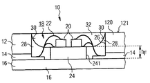
図1のオプトエレクトロニクス素子10では、キャビティ18を備えたベースケーシング12はリードフレーム14を適切なプラスティック材料で包囲するように射出成型することにより構成されている。
【0028】
キャビティ18内には、リードフレーム14上に電磁放射を放出および/または受信する半導体チップ20、例えば発光ダイオードチップが存在している。このチップは少なくとも一部の放射をサイドエッジを介して放出および/または受信する。半導体チップ20はボンディングワイヤ22を介してリードフレーム14の電気端子に接続されている。半導体チップ20とキャビティ側壁26とのあいだには反射性の充填物質28が充填されており、この物質は例えばTiO2粒子を充填されたエポキシド樹脂である。ここで充填物質28中のTiO2成分は充填物質の反射能を高めることのできる量であり、有利には充填物質28中のTiO2成分は約10vol%〜50vol%である。二酸化チタン粒子、二酸化ジルコニウム粒子、酸化亜鉛粒子、硫酸バリウム粒子、窒化ガリウム粒子、および/またはこれらの粒子の組み合わせが、充填物質でエポキシド樹脂とともに使用されるのに適している。重要なのはエポキシド樹脂の屈折率とこれらの粒子の屈折率との差が充分に大きく、充填物質28の反射能が高められるということである。
【0029】
ベースケーシング12のフロント面121へ向かう充填物質の表面30は半導体チップ20から見て凹状に湾曲しており、放出および/または受信される放射の少なくとも一部に対するリフレクタ面を形成している。これに代えてオプトエレクトロニクス素子10のジオメトリまたは半導体チップの放出特性によっては半導体チップから見て凸形のリフレクタ面を構成することもできる。
【0030】
半導体チップ20に加えてこれとベースケーシング12とのあいだに図示されていない別のチップ支持体基板を配置することもできる。チップ支持体基板の寸法はサイドエッジとキャビティ側壁26とのあいだに充填物質28を充填するためのトレンチが生じるように選定される。
【0031】
キャビティ底面に対する充填物質の充填高さhFは、半導体チップの近傍では当該の半導体チップの底面から放出および/または受信を行う領域までの距離よりも小さい。いっぽうキャビティの側壁へ向かっては、充填高さhFは上述の距離を越えて大きくなる。
【0032】
充填物質の上方に存在する半導体チップ20の表面の露出領域は放射透過性のカプセル化物質32によってカバーされる。このカプセル化物質は例えばエポキシド樹脂または他の適切な反応性樹脂から成る。
【0033】
図2の実施例では、外部電気端子14は例えばアルミニウムから成る支持体ボディ16上に被着されている。キャビティ18は同様に支持体ボディ16上に配置されたプラスティックのケーシングフレーム120によって形成されている。
【0034】
キャビティ内では、電磁放射を放出および/または受信する2つの半導体チップ20、例えば2つの発光ダイオードチップ(LEDチップ)がチップ支持体基板24上に実装されている。このチップ支持体基板は例えばシリコンから成る。2つのLEDチップはボンディングワイヤ22を介して外部電気端子14に導電接続されている。
【0035】
図2の断面図から明らかなように、キャビティ18の内面は第1の実施例と同様にほぼ円筒状である。つまりこのキャビティは底面からベースケーシング12のフロント面へ向かってきわめて急峻に延在している。こうした急峻な側壁26は無視できるほどの小さなリフレクタ作用しか有さない。
【0036】
キャビティ側壁26の急峻性を低減して底面をそのままにすると、チップおよび必要面積の寸法および個数によってチップ実装時およびコンタクト接続時に固定に設定されるキャビティの最小寸法が大きくなり、構造寸法が増大してしまう。これは多くのアプリケーションでスペース不足を引き起こすため回避すべきである。この問題も本発明によって解決される。
【0037】
図2の実施例においても、キャビティ18にはチップ支持体基板24とキャビティ側壁26とのあいだのトレンチの領域に充填物質28が充填されている。この充填物質28は図1に示された第1の実施例と同じ材料から成っている。
【0038】
図2の断面図から明らかなように、充填物質28の充填高さhFは、半導体チップ20すなわちチップ支持体基板24の近傍ではキャビティ側壁26近傍でよりも格段に小さい。キャビティ側壁近傍では充填物質28がほぼベースケーシング12のフロント面121のエッジまで盛り上がる。このようにしてフロント面へ向かってほぼパラボラ状に開放した形状の充填物質28の表面が得られる。この形状は、材料および充填物質28の用量を適切に選択すれば、充填物質28とケーシング120の材料とのあいだの接着力により自動的に生じる。半導体チップ20から見ると凹形に湾曲した充填物質28の内面30は、半導体チップ20の側方から放出および/または受信される放射のリフレクタとして用いられる。
【0039】
TiO2成分を含む充填物質28の反射能は約80%である。キャビティが透過性の充填物質のみで充填された他のオプトエレクトロニクス素子に比べて、本発明のオプトエレクトロニクス素子によれば、外部効率を20%以上増大することができる。
【0040】
半導体チップ20を保護するために、キャビティ18には放射透過性の例えば透明なカプセル化物質32が充填される。このカプセル化物質は半導体チップ20をカバーし、半導体チップ20から放出および/または受信される放射を透過する。このカプセル化物質32については、従来技術の素子で使用されている充填物質と同様の透明な樹脂、例えばエポキシド樹脂またはポリカーボネートを使用することができる。これは有利には充填物質28の特性に適合化される(このことは図1の実施例にも当てはまる)。
【0041】
ベースケーシング12のキャビティ18内に配置される半導体チップ20の個数はもちろん1つまたは2つに限定されない。キャビティ内に2つ以上の半導体チップを実装することができる。またベースケーシング12内には1つ以上のキャビティ18を形成することができる。
【0042】
第1の実施例または第2の実施例のオプトエレクトロニクス素子を製造するためには、まずキャビティ18を備えたベースケーシング12を形成し、次に半導体チップ20をキャビティ18内に実装し、これと外部電気端子14とを導電接続する。続いて充填物質28をキャビティ18内に充填する。これは次の容量で行われる。すなわち
i)キャビティ18の底面に対する充填物質28の充填高さhFが半導体チップ20の近傍では当該の半導体チップの底面から放出および/または受信を行う領域までの距離よりも小さくなり、
ii)その表面が半導体チップ20から見るとキャビティ側壁26の個所で、充填物質28の材料と側壁26の材料とのあいだの接着性により盛り上がり、凹形に湾曲する
ように選定される。
【0043】
このようにして放射に対するリフレクタとなる表面30が形成される。
【0044】
続いて放射透過性のカプセル化物質32がキャビティ18内に充填される。このカプセル化物質は少なくとも先行のステップの後になお露出している半導体チップ20の表面をカバーする。
【0045】
本発明を実施例に則して説明したが、もちろん本発明は上述の実施例のみに限定されるものではない。独立請求項1、14に示されている本発明の概念は多数の実施態様として適用可能である。
【図面の簡単な説明】
【図1】第1の実施例の概略的な断面図である。
【図2】第1の実施例の概略的な断面図である。
【符号の説明】
10 オプトエレクトロニクス素子
12 ベースケーシング
120 ケーシングフレーム
121 フロント面
14 リードフレーム
16 支持体ボディ
18 キャビティ
20 半導体チップ
22 ボンディングワイヤ
24 チップ支持体基板
241 サイドエッジ
26 キャビティ側壁
28 充填物質
30 内面
32 カプセル化物質
【発明の属する技術分野】
本発明は、少なくとも1つのキャビティを有するベースケーシングおよびキャビティ内に配置された少なくとも1つの電磁放射を放出および/または受信する半導体チップを有しており、前記キャビティはベースケーシングのフロント面からベースケーシング内へ延在しているオプトエレクトロニクス素子、特に表面実装可能なオプトエレクトロニクス素子に関する。
【0002】
本発明はさらに、前述のオプトエレクトロニクス素子の製造方法に関する。
【0003】
【従来の技術】
従来、表面実装可能なオプトエレクトロニクス素子を製造する際には、例えばまず予め成形された導電性のリードフレームが適切なプラスティック材料で包囲するように射出成型され、素子のベースケーシングが形成される。このベースケーシングはキャビティ(またはチップウィンドウ)を有しており、このキャビティ内に対向する2つの側からリードフレーム端子が案内される。リードフレーム端子には電磁放射を放出または送信する半導体チップ、例えばLEDチップが接着され、電気的にコンタクトされる。キャビティ内には透明または透光性の鋳込物質が充填される。表面実装可能なオプトエレクトロニクス素子の基本的な形態は例えば刊行物 F.Moeller & G. Waitl, ”SIEMENS SMT−TOPLED fuer die Oberflaechenmontage”, Siemens Components 29 (1991), Heft 4 147頁〜149頁から知られる。
【0004】
この種のオプトエレクトロニクス素子では、外部効率を高めるために、キャビティに斜めの内面を設け、これをリフレクタとして用いることが通常である。内面の傾角に応じてキャビティの開口も相応に拡大される。
【0005】
この種のリフレクタ装置を備えたオプトエレクトロニクス素子の例は、独国特許出願公開第19755734号明細書および独国特許出願公開第19918370号明細書に記載されている。
【0006】
類似の構造は独国特許出願公開第19536454号明細書にも記載されている。この場合は素子のベースケーシングのキャビティに金属チップ支持体が設けられており、その上に半導体チップが実装されている。チップ支持体では半導体チップの固定された領域にウェルが形成され、その内面が反転した円錐台にほぼ相応する形状を有しており、これが半導体チップから放出された放射に対するリフレクタとなる。
【0007】
オプトエレクトロニクス素子の微細化が進むにつれて、できるかぎり小さいキャビティ開口を設けること、および/またはキャビティ内にいっそう複雑な半導体チップを設けて配線することへの要求がますます高まってきている。この場合キャビティの側壁はスペース不足のためにキャビティの底面に対して垂直または急峻な角度とならざるを得ない。
【0008】
ランベルトの法則に基づく放射受信特性または後方へ向かう半導体チップの放射受信特性のために、光電流の明らかな損失が生じ、素子の外部効率が低下する。したがって実現困難であるにもかかわらず、キャビティ内面にリフレクタを設けて充分に良好な効率を得ようとするオプトエレクトロニクス素子への要求が存在する。
【0009】
【特許文献1】
独国特許出願公開第19755734号明細書
【特許文献2】
独国特許出願公開第19918370号明細書
【特許文献3】
独国特許出願公開第19536454号明細書
【非特許文献1】
F.Moeller & G. Waitl, ”SIEMENS SMT−TOPLED fuer die Oberflaechenmontage”, Siemens Components 29 (1991), Heft 4 147頁〜149頁
【0010】
【発明が解決しようとする課題】
本発明の課題は、広汎な要求を満足する冒頭に言及した形式のオプトエレクトロニクス素子およびその製造方法を提供することである。
【0011】
【課題を解決するための手段】
この課題は、キャビティ内の半導体チップとキャビティ側壁とのあいだに反射性の充填物質が配置されており、ベースケーシングのフロント面へ向かう少なくとも1つの表面は半導体チップから見て凹面鏡状すなわち凹形に湾曲しており、一部の放射に対するリフレクタ面を形成している構成により解決される。
【0012】
課題はまた、キャビティの底面に対する充填物質の充填高さhFが半導体チップの近傍では当該の半導体チップの底面から放出および/または受信を行う領域までの距離よりも小さくなり、表面が半導体チップから見るとキャビティ側壁へ向かって充填物質の材料と側壁の材料とのあいだの接着性により凹状に湾曲して放射用のリフレクタを形成するように、充填物質の材料および量を選定することにより解決される。
【0013】
【発明の実施の形態】
本発明の請求項1に記載の特徴を有するオプトエレクトロニクス素子、および本発明の請求項14に記載の特徴を有するオプトエレクトロニクス素子の製造方法により、前述の課題は解決される。オプトエレクトロニクス素子およびその製造方法についての他の有利な実施形態および改善形態は従属請求項に記載されている。
【0014】
本発明のオプトエレクトロニクス素子はベースケーシングと放射を放出および/または受信する少なくとも1つの半導体チップとをベースケーシングのキャビティ内に有している。リフレクタは、従来のオプトエレクトロニクス素子とは異なり、ベースケーシングの反射性のキャビティ側壁のみによるのではなく、一部はキャビティ内に充填される反射性の充填物質によっても実現される。充填物質の材料および量は、有利には、充填の際に、これとキャビティ側壁の材料とのあいだの接着力により充填物質がキャビティ側壁に向かって盛り上がり、凹形すなわちパラボラ状の表面を形成するように選定されている。ケーシングのフロント面へ向かう充填物質の当該の表面は、半導体チップから放出および/または受信される電磁放射に対するリフレクタ面となる。充填物質の組成は、リフレクタ面でできる限り多くの放射成分が全反射するように選定されている。これは充填物質として適切な屈折率を有する材料を使用することにより達成される。
【0015】
換言すれば、キャビティが充填物質で部分的に充填され、充填物質とベースケーシングとのあいだの接着力によって自動的に半導体チップから見てほぼ凹状のキャビティ内面が生じる。これは充填物質がベースケーシングのキャビティの側面へ向かって盛り上がるためである。このようにして形成されたパラボラ状の充填物質の内面がキャビティ内で使用される半導体チップに対するリフレクタを形成する。
【0016】
当該のリフレクタ面はキャビティ開口がきわめて小さい場合にも充填物質の用量を適切に調整することにより簡単に形成することができる。さらにキャビティ内に存在する端子、ワイヤおよびその他は、充填物質によって機能を損なうことなくカバーされる。
【0017】
したがって本発明の手段によれば、オプトエレクトロニクス素子において、キャビティの開口を狭くすること、および/またはキャビティ内に複雑な半導体チップおよび配線を設けることによりリフレクタを形成し、素子の外部効率を高めることができる。
【0018】
本発明の有利な実施形態では、充填物質の材料は二酸化チタンTiO2を含む。特に有利には充填物質の材料はTiO2粒子を充填されたエポキシド樹脂である。特に有利には充填物質28のTiO2成分は10Vol%〜50Vol%である。
【0019】
従来のオプトエレクトロニクス素子と同様に、有利にはキャビティ内へチップを実装し、チップと外部電気端子とを例えばボンディングワイヤを介して接続し、充填物質を充填した後に残るチップの露出表面が放射透過性の(例えば透明な)カプセル化物質でカバーされる。これにより半導体チップがカバーされ、有利にはキャビティの大部分が充填される。
【0020】
本発明のオプトエレクトロニクス素子の製造方法の有利な実施形態では、ベースケーシングとこのベースケーシングのキャビティ内に配置された少なくとも1つの半導体チップとを備えたオプトエレクトロニクス素子を製造するために、
(a)リードフレームの周囲にベースケーシングを形成する。その際にベースケーシング内へリードフレーム端子を案内するキャビティを設ける。
【0021】
(b)放射を放出または受信する少なくとも1つの半導体チップをキャビティ内に配置し、これについて電気コンタクトを形成する。
【0022】
(c)部分的に充填物質をキャビティ内に充填する。ここで充填物質の材料および量は、充填物質の材料と側壁の材料とのあいだの接着性により、下方から上方へ向かってほぼ円錐状にひろがる形状をとり、この円錐状の内面が放射用のリフレクタを形成するように選定される。
【0023】
有利には、続いて次の方法ステップ(d)で放射透過性、例えば透明のカプセル化物質がキャビティ内に充填され、キャビティ内の半導体チップが完全にカバーされる。
【0024】
エポキシド樹脂とこれに含まれるTiO2成分とをベースとした充填物質の反射能は約80%である。同じ構造であるが本発明のような充填物質をキャビティ内に有さず、半導体チップに対して透明なカプセル化物質のみを有する従来のオプトエレクトロニクス素子と比べると、本発明の充填物質では外部効率の20%以上の向上を達成することができる。
【0025】
【実施例】
本発明のオプトエレクトロニクス素子およびこの素子の製造方法の別の利点および有利な実施形態を図1、図2に示された実施例に則して以下に説明する。
【0026】
2つの実施例では同じまたは類似の機能を有する素子には同じ参照番号を付してある。
【0027】
図1のオプトエレクトロニクス素子10では、キャビティ18を備えたベースケーシング12はリードフレーム14を適切なプラスティック材料で包囲するように射出成型することにより構成されている。
【0028】
キャビティ18内には、リードフレーム14上に電磁放射を放出および/または受信する半導体チップ20、例えば発光ダイオードチップが存在している。このチップは少なくとも一部の放射をサイドエッジを介して放出および/または受信する。半導体チップ20はボンディングワイヤ22を介してリードフレーム14の電気端子に接続されている。半導体チップ20とキャビティ側壁26とのあいだには反射性の充填物質28が充填されており、この物質は例えばTiO2粒子を充填されたエポキシド樹脂である。ここで充填物質28中のTiO2成分は充填物質の反射能を高めることのできる量であり、有利には充填物質28中のTiO2成分は約10vol%〜50vol%である。二酸化チタン粒子、二酸化ジルコニウム粒子、酸化亜鉛粒子、硫酸バリウム粒子、窒化ガリウム粒子、および/またはこれらの粒子の組み合わせが、充填物質でエポキシド樹脂とともに使用されるのに適している。重要なのはエポキシド樹脂の屈折率とこれらの粒子の屈折率との差が充分に大きく、充填物質28の反射能が高められるということである。
【0029】
ベースケーシング12のフロント面121へ向かう充填物質の表面30は半導体チップ20から見て凹状に湾曲しており、放出および/または受信される放射の少なくとも一部に対するリフレクタ面を形成している。これに代えてオプトエレクトロニクス素子10のジオメトリまたは半導体チップの放出特性によっては半導体チップから見て凸形のリフレクタ面を構成することもできる。
【0030】
半導体チップ20に加えてこれとベースケーシング12とのあいだに図示されていない別のチップ支持体基板を配置することもできる。チップ支持体基板の寸法はサイドエッジとキャビティ側壁26とのあいだに充填物質28を充填するためのトレンチが生じるように選定される。
【0031】
キャビティ底面に対する充填物質の充填高さhFは、半導体チップの近傍では当該の半導体チップの底面から放出および/または受信を行う領域までの距離よりも小さい。いっぽうキャビティの側壁へ向かっては、充填高さhFは上述の距離を越えて大きくなる。
【0032】
充填物質の上方に存在する半導体チップ20の表面の露出領域は放射透過性のカプセル化物質32によってカバーされる。このカプセル化物質は例えばエポキシド樹脂または他の適切な反応性樹脂から成る。
【0033】
図2の実施例では、外部電気端子14は例えばアルミニウムから成る支持体ボディ16上に被着されている。キャビティ18は同様に支持体ボディ16上に配置されたプラスティックのケーシングフレーム120によって形成されている。
【0034】
キャビティ内では、電磁放射を放出および/または受信する2つの半導体チップ20、例えば2つの発光ダイオードチップ(LEDチップ)がチップ支持体基板24上に実装されている。このチップ支持体基板は例えばシリコンから成る。2つのLEDチップはボンディングワイヤ22を介して外部電気端子14に導電接続されている。
【0035】
図2の断面図から明らかなように、キャビティ18の内面は第1の実施例と同様にほぼ円筒状である。つまりこのキャビティは底面からベースケーシング12のフロント面へ向かってきわめて急峻に延在している。こうした急峻な側壁26は無視できるほどの小さなリフレクタ作用しか有さない。
【0036】
キャビティ側壁26の急峻性を低減して底面をそのままにすると、チップおよび必要面積の寸法および個数によってチップ実装時およびコンタクト接続時に固定に設定されるキャビティの最小寸法が大きくなり、構造寸法が増大してしまう。これは多くのアプリケーションでスペース不足を引き起こすため回避すべきである。この問題も本発明によって解決される。
【0037】
図2の実施例においても、キャビティ18にはチップ支持体基板24とキャビティ側壁26とのあいだのトレンチの領域に充填物質28が充填されている。この充填物質28は図1に示された第1の実施例と同じ材料から成っている。
【0038】
図2の断面図から明らかなように、充填物質28の充填高さhFは、半導体チップ20すなわちチップ支持体基板24の近傍ではキャビティ側壁26近傍でよりも格段に小さい。キャビティ側壁近傍では充填物質28がほぼベースケーシング12のフロント面121のエッジまで盛り上がる。このようにしてフロント面へ向かってほぼパラボラ状に開放した形状の充填物質28の表面が得られる。この形状は、材料および充填物質28の用量を適切に選択すれば、充填物質28とケーシング120の材料とのあいだの接着力により自動的に生じる。半導体チップ20から見ると凹形に湾曲した充填物質28の内面30は、半導体チップ20の側方から放出および/または受信される放射のリフレクタとして用いられる。
【0039】
TiO2成分を含む充填物質28の反射能は約80%である。キャビティが透過性の充填物質のみで充填された他のオプトエレクトロニクス素子に比べて、本発明のオプトエレクトロニクス素子によれば、外部効率を20%以上増大することができる。
【0040】
半導体チップ20を保護するために、キャビティ18には放射透過性の例えば透明なカプセル化物質32が充填される。このカプセル化物質は半導体チップ20をカバーし、半導体チップ20から放出および/または受信される放射を透過する。このカプセル化物質32については、従来技術の素子で使用されている充填物質と同様の透明な樹脂、例えばエポキシド樹脂またはポリカーボネートを使用することができる。これは有利には充填物質28の特性に適合化される(このことは図1の実施例にも当てはまる)。
【0041】
ベースケーシング12のキャビティ18内に配置される半導体チップ20の個数はもちろん1つまたは2つに限定されない。キャビティ内に2つ以上の半導体チップを実装することができる。またベースケーシング12内には1つ以上のキャビティ18を形成することができる。
【0042】
第1の実施例または第2の実施例のオプトエレクトロニクス素子を製造するためには、まずキャビティ18を備えたベースケーシング12を形成し、次に半導体チップ20をキャビティ18内に実装し、これと外部電気端子14とを導電接続する。続いて充填物質28をキャビティ18内に充填する。これは次の容量で行われる。すなわち
i)キャビティ18の底面に対する充填物質28の充填高さhFが半導体チップ20の近傍では当該の半導体チップの底面から放出および/または受信を行う領域までの距離よりも小さくなり、
ii)その表面が半導体チップ20から見るとキャビティ側壁26の個所で、充填物質28の材料と側壁26の材料とのあいだの接着性により盛り上がり、凹形に湾曲する
ように選定される。
【0043】
このようにして放射に対するリフレクタとなる表面30が形成される。
【0044】
続いて放射透過性のカプセル化物質32がキャビティ18内に充填される。このカプセル化物質は少なくとも先行のステップの後になお露出している半導体チップ20の表面をカバーする。
【0045】
本発明を実施例に則して説明したが、もちろん本発明は上述の実施例のみに限定されるものではない。独立請求項1、14に示されている本発明の概念は多数の実施態様として適用可能である。
【図面の簡単な説明】
【図1】第1の実施例の概略的な断面図である。
【図2】第1の実施例の概略的な断面図である。
【符号の説明】
10 オプトエレクトロニクス素子
12 ベースケーシング
120 ケーシングフレーム
121 フロント面
14 リードフレーム
16 支持体ボディ
18 キャビティ
20 半導体チップ
22 ボンディングワイヤ
24 チップ支持体基板
241 サイドエッジ
26 キャビティ側壁
28 充填物質
30 内面
32 カプセル化物質
Claims (15)
- 少なくとも1つのキャビティ(18)を有するベースケーシング(12)およびキャビティ(18)内に配置された少なくとも1つの電磁放射を放出および/または受信する半導体チップ(20)を有しており、
前記キャビティ(18)がベースケーシング(12)のフロント面(121)からベースケーシング(12)内へ延在している
オプトエレクトロニクス素子(10)において、
キャビティ(18)内の半導体チップ(20)とキャビティ側壁(26)とのあいだに反射性の充填物質(28)が配置されており、
ベースケーシング(12)のフロント面(121)へ向かう少なくとも1つの表面(30)は半導体チップ(20)から見て凹面鏡状すなわち凹形に湾曲しており、一部の放射に対するリフレクタ面を形成している
ことを特徴とするオプトエレクトロニクス素子。 - 半導体チップ(20)とベースケーシング(12)とのあいだにチップ支持体基板(24)が配置されており、該基板の寸法はサイドエッジ(241)とキャビティ側壁(26)とのあいだに充填物質(28)を収容するためのトレンチが形成されるように選定されている、請求項1記載の素子。
- キャビティ(18)の底面に対する充填物質(28)の充填高さhFは、半導体チップ(20)の近傍では当該の半導体チップの底面から放出および/または受信を行う領域までの距離よりも小さく、キャビティ側壁へ向かって前記距離を越えて大きくなる、請求項1または2記載の素子。
- 充填物質(28)の材料の一部の粒子は残りの材料よりも高い屈折率を有する、請求項1から3までのいずれか1項記載の素子。
- 充填物質(28)はエポキシド樹脂と該樹脂よりも高い屈折率を有する粒子とを有する、請求項4記載の素子。
- 充填物質(28)中の粒子は二酸化チタン粒子、二酸化ジルコニウム粒子、酸化亜鉛粒子、硫酸バリウム粒子、窒化ガリウム粒子、および/またはこれらの粒子の組み合わせである、請求項4または5記載の素子。
- 充填物質(28)中の粒子の成分量は充填物質の反射性が高まるように選定されている、請求項6記載の素子。
- 充填物質(28)中の二酸化チタン粒子の成分量は約10Vol%〜50Vol%である、請求項6または7記載の素子。
- 半導体チップ(20)は放射透過性のカプセル化物質(32)によって少なくとも部分的にカプセル化されている、請求項1から8までのいずれか1項記載の素子。
- ベースケーシング(12)は支持体ボディ(16)を有しており、該ボディにはキャビティ(18)を形成するケーシングフレーム(120)と、キャビティ(18)内に達する半導体チップ(20)用の外部電気端子(14)とが配置されている、請求項1から9までのいずれか1項記載の素子。
- 支持体ボディ(16)およびチップ支持体基板(24)は良好な熱伝導性を有する材料から成型されている、請求項2から10までのいずれか1項記載の素子。
- 支持体ボディ(16)は主として金属材料を有している、請求項9記載の素子。
- チップ支持体基板(24)は主としてシリコンを有している、請求項11または12記載の素子。
- (a)キャビティ(18)を備えたベースケーシング(12)を形成するステップと、
(b)半導体チップ(20)をキャビティ(18)内に配置するステップと、
(c)充填物質(28)をキャビティ(18)内に充填するステップとを有する請求項1から13までのいずれか1項記載のオプトエレクトロニクス素子(10)の製造方法において、
キャビティ(18)の底面に対する充填物質(28)の充填高さhFが半導体チップ(20)の近傍では当該の半導体チップの底面から放出および/または受信を行う領域までの距離よりも小さくなり、表面が半導体チップ(20)から見るとキャビティ側壁(26)へ向かって充填物質(28)の材料と側壁(26)の材料とのあいだの接着性により凹状に湾曲して放射用のリフレクタを形成するように、充填物質(28)の材料および量を選定する
ことを特徴とするオプトエレクトロニクス素子の製造方法。 - 充填物質(28)の充填後に放射透過性のカプセル化物質(32)をキャビティ(18)内に充填し、先行のステップを経てなお露出している半導体チップ(20)の表面を少なくともカバーする、請求項14記載の方法。
Applications Claiming Priority (1)
| Application Number | Priority Date | Filing Date | Title |
|---|---|---|---|
| DE10229067A DE10229067B4 (de) | 2002-06-28 | 2002-06-28 | Optoelektronisches Bauelement und Verfahren zu dessen Herstellung |
Publications (1)
| Publication Number | Publication Date |
|---|---|
| JP2004040099A true JP2004040099A (ja) | 2004-02-05 |
Family
ID=29761526
Family Applications (1)
| Application Number | Title | Priority Date | Filing Date |
|---|---|---|---|
| JP2003182480A Pending JP2004040099A (ja) | 2002-06-28 | 2003-06-26 | オプトエレクトロニクス素子およびオプトエレクトロニクス素子の製造方法 |
Country Status (3)
| Country | Link |
|---|---|
| US (6) | US6900511B2 (ja) |
| JP (1) | JP2004040099A (ja) |
| DE (1) | DE10229067B4 (ja) |
Cited By (36)
| Publication number | Priority date | Publication date | Assignee | Title |
|---|---|---|---|---|
| JP2005136379A (ja) * | 2003-10-08 | 2005-05-26 | Nichia Chem Ind Ltd | 半導体装置 |
| JP2006135300A (ja) * | 2004-10-04 | 2006-05-25 | Stanley Electric Co Ltd | 半導体発光装置の製造方法 |
| WO2006107012A1 (ja) * | 2005-04-04 | 2006-10-12 | Nippon Sheet Glass Company, Limited | 発光ユニット、該発光ユニットを用いた照明装置及び画像読取装置 |
| JP2007184425A (ja) * | 2006-01-06 | 2007-07-19 | Shinko Electric Ind Co Ltd | 発光装置及びその製造方法 |
| JP2007201392A (ja) * | 2005-04-27 | 2007-08-09 | Kyocera Corp | 発光素子搭載用基体ならびにこれを用いた発光装置 |
| WO2007100037A1 (ja) * | 2006-03-02 | 2007-09-07 | Sony Chemical & Information Device Corporation | 機能素子実装モジュール及びその製造方法 |
| JP2008060344A (ja) * | 2006-08-31 | 2008-03-13 | Toshiba Corp | 半導体発光装置 |
| JP2009064842A (ja) * | 2007-09-04 | 2009-03-26 | Sumitomo Metal Electronics Devices Inc | セラミックス焼結体およびそれを用いた基板およびそれを用いた発光素子搭載用パッケージおよびそれを用いた発光装置 |
| JP2009272369A (ja) * | 2008-05-01 | 2009-11-19 | Nec Lighting Ltd | 発光装置およびその製造方法 |
| JP2010199547A (ja) * | 2009-01-30 | 2010-09-09 | Nichia Corp | 発光装置及びその製造方法 |
| KR100987152B1 (ko) | 2008-11-12 | 2010-10-11 | (주) 아모엘이디 | 반도체 패키지 |
| JP2010235753A (ja) * | 2009-03-31 | 2010-10-21 | Hitachi Chem Co Ltd | 光反射用熱硬化性樹脂組成物、光半導体素子搭載用基板及びその製造方法、並びに光半導体装置 |
| JP2011191785A (ja) * | 2005-03-29 | 2011-09-29 | Kyocera Corp | 反射部材、これを用いた発光装置および照明装置 |
| JP2012089728A (ja) * | 2010-10-21 | 2012-05-10 | Nichia Chem Ind Ltd | 発光装置及びその製造方法 |
| JP2012151436A (ja) * | 2010-11-05 | 2012-08-09 | Rohm Co Ltd | 半導体発光装置 |
| US8373182B2 (en) | 2010-09-09 | 2013-02-12 | Stanley Electric Co., Ltd. | Semiconductor light-emitting device and manufacturing method |
| JP2013051431A (ja) * | 2012-10-25 | 2013-03-14 | Nichia Chem Ind Ltd | 発光装置 |
| US8455907B2 (en) | 2010-06-16 | 2013-06-04 | Stanley Electric Co., Ltd. | Semiconductor light emitting device having an optical plate including a meniscus control structure and method of manufacturing |
| US8461610B2 (en) | 2010-06-16 | 2013-06-11 | Stanley Electric Co., Ltd. | Semiconductor light emitting device having a reflective material with a side slant surface and method of manufacturing |
| JP2013149906A (ja) * | 2012-01-23 | 2013-08-01 | Stanley Electric Co Ltd | 発光装置、車両用灯具及び発光装置の製造方法 |
| JP2013168685A (ja) * | 2013-06-03 | 2013-08-29 | Nichia Chem Ind Ltd | 発光装置 |
| US8581287B2 (en) | 2011-01-24 | 2013-11-12 | Stanley Electric Co., Ltd. | Semiconductor light emitting device having a reflective material, wavelength converting layer and optical plate with rough and plane surface regions, and method of manufacturing |
| JPWO2012050110A1 (ja) * | 2010-10-12 | 2014-02-24 | ローム株式会社 | Ledモジュール |
| US8921877B2 (en) | 2010-08-02 | 2014-12-30 | Stanley Electric Co., Ltd. | Semiconductor light-emitting device for producing wavelength-converted light and method for manufacturing the same |
| US9024343B2 (en) | 2007-12-28 | 2015-05-05 | Nichia Corporation | Light emitting device |
| JP2015225942A (ja) * | 2014-05-28 | 2015-12-14 | サンケン電気株式会社 | 発光装置 |
| JP2016072412A (ja) * | 2014-09-30 | 2016-05-09 | 日亜化学工業株式会社 | 発光装置及び発光装置の製造方法 |
| US9368690B2 (en) | 2013-01-24 | 2016-06-14 | Stanley Electric Co., Ltd. | Semiconductor light-emitting device |
| JP2016213505A (ja) * | 2016-09-07 | 2016-12-15 | 日亜化学工業株式会社 | 発光装置用パッケージ成形体及びそれを用いた発光装置 |
| JP2017069394A (ja) * | 2015-09-30 | 2017-04-06 | ローム株式会社 | Led照明器具およびその製造方法 |
| US9859480B2 (en) | 2015-08-20 | 2018-01-02 | Nichia Corporation | Light emitting device and method of manufacturing light emitting device |
| US9893255B2 (en) | 2012-01-20 | 2018-02-13 | Nichia Corporation | Molded package and light emitting device |
| JP2019017734A (ja) * | 2017-07-18 | 2019-02-07 | 新日本無線株式会社 | 発光装置及びその製造方法 |
| JP2019117850A (ja) * | 2017-12-27 | 2019-07-18 | 日亜化学工業株式会社 | 発光装置及びその製造方法 |
| JP2020205355A (ja) * | 2019-06-18 | 2020-12-24 | スタンレー電気株式会社 | 発光装置 |
| JP2021061444A (ja) * | 2021-01-12 | 2021-04-15 | 日亜化学工業株式会社 | 発光装置 |
Families Citing this family (125)
| Publication number | Priority date | Publication date | Assignee | Title |
|---|---|---|---|---|
| DE10131698A1 (de) * | 2001-06-29 | 2003-01-30 | Osram Opto Semiconductors Gmbh | Oberflächenmontierbares strahlungsemittierendes Bauelement und Verfahren zu dessen Herstellung |
| DE10229067B4 (de) * | 2002-06-28 | 2007-08-16 | Osram Opto Semiconductors Gmbh | Optoelektronisches Bauelement und Verfahren zu dessen Herstellung |
| DE10245930A1 (de) * | 2002-09-30 | 2004-04-08 | Osram Opto Semiconductors Gmbh | Optoelektronisches Bauelement und Bauelement-Modul |
| DE10245945A1 (de) | 2002-09-30 | 2004-04-08 | Osram Opto Semiconductors Gmbh | Lichtquellenmodul sowie Verfahren zu dessen Herstellung |
| KR101059361B1 (ko) * | 2003-01-16 | 2011-08-24 | 파나소닉 주식회사 | 리드 프레임 및 반도체 발광장치 |
| TWM271252U (en) * | 2004-12-14 | 2005-07-21 | Niching Ind Corp | Package structure of light-emitting device |
| DE102004014207A1 (de) * | 2004-03-23 | 2005-10-13 | Osram Opto Semiconductors Gmbh | Optoelektronisches Bauteil mit mehrteiligem Gehäusekörper |
| US7476913B2 (en) * | 2004-08-10 | 2009-01-13 | Renesas Technology Corp. | Light emitting device having a mirror portion |
| JP4756841B2 (ja) | 2004-09-29 | 2011-08-24 | スタンレー電気株式会社 | 半導体発光装置の製造方法 |
| TWM271255U (en) * | 2004-10-08 | 2005-07-21 | Bright Led Electronics Corp | High-power surface-mounted light-emitting diode with high heat dissipation property |
| US9070850B2 (en) * | 2007-10-31 | 2015-06-30 | Cree, Inc. | Light emitting diode package and method for fabricating same |
| US7821023B2 (en) | 2005-01-10 | 2010-10-26 | Cree, Inc. | Solid state lighting component |
| US9793247B2 (en) | 2005-01-10 | 2017-10-17 | Cree, Inc. | Solid state lighting component |
| JP2006313321A (ja) * | 2005-04-04 | 2006-11-16 | Nippon Sheet Glass Co Ltd | 発光ユニット、該発光ユニットを用いた照明装置及び画像読取装置 |
| US8669572B2 (en) * | 2005-06-10 | 2014-03-11 | Cree, Inc. | Power lamp package |
| KR101161383B1 (ko) * | 2005-07-04 | 2012-07-02 | 서울반도체 주식회사 | 발광 다이오드 및 이를 제조하기 위한 방법 |
| DE102006032415A1 (de) | 2005-09-30 | 2007-04-05 | Osram Opto Semiconductors Gmbh | Verfahren zur Herstellung eines strahlungsemittierenden Bauelements und strahlungsemittierendes Bauelement |
| JP2009530798A (ja) | 2006-01-05 | 2009-08-27 | イルミテックス, インコーポレイテッド | Ledから光を導くための独立した光学デバイス |
| US8044412B2 (en) | 2006-01-20 | 2011-10-25 | Taiwan Semiconductor Manufacturing Company, Ltd | Package for a light emitting element |
| US20070181897A1 (en) * | 2006-02-03 | 2007-08-09 | Been-Yu Liaw | High heat dissipating package baseplate for a high brightness LED |
| US7675145B2 (en) * | 2006-03-28 | 2010-03-09 | Cree Hong Kong Limited | Apparatus, system and method for use in mounting electronic elements |
| US9780268B2 (en) | 2006-04-04 | 2017-10-03 | Cree, Inc. | Submount based surface mount device (SMD) light emitter components and methods |
| US8748915B2 (en) * | 2006-04-24 | 2014-06-10 | Cree Hong Kong Limited | Emitter package with angled or vertical LED |
| US7635915B2 (en) * | 2006-04-26 | 2009-12-22 | Cree Hong Kong Limited | Apparatus and method for use in mounting electronic elements |
| WO2007139781A2 (en) * | 2006-05-23 | 2007-12-06 | Cree Led Lighting Solutions, Inc. | Lighting device |
| TWI321857B (en) * | 2006-07-21 | 2010-03-11 | Epistar Corp | A light emitting device |
| US8735920B2 (en) | 2006-07-31 | 2014-05-27 | Cree, Inc. | Light emitting diode package with optical element |
| US20080029775A1 (en) * | 2006-08-02 | 2008-02-07 | Lustrous Technology Ltd. | Light emitting diode package with positioning groove |
| US8367945B2 (en) * | 2006-08-16 | 2013-02-05 | Cree Huizhou Opto Limited | Apparatus, system and method for use in mounting electronic elements |
| US7789531B2 (en) | 2006-10-02 | 2010-09-07 | Illumitex, Inc. | LED system and method |
| DE102006048230B4 (de) | 2006-10-11 | 2012-11-08 | Osram Ag | Leuchtdiodensystem, Verfahren zur Herstellung eines solchen und Hinterleuchtungseinrichtung |
| TW200826311A (en) * | 2006-12-04 | 2008-06-16 | Prolight Opto Technology Corp | Side emitting LED |
| DE102007001706A1 (de) | 2007-01-11 | 2008-07-17 | Osram Opto Semiconductors Gmbh | Gehäuse für optoelektronisches Bauelement und Anordnung eines optoelektronischen Bauelementes in einem Gehäuse |
| JP5102051B2 (ja) * | 2007-01-18 | 2012-12-19 | シチズン電子株式会社 | 半導体発光装置 |
| US9711703B2 (en) * | 2007-02-12 | 2017-07-18 | Cree Huizhou Opto Limited | Apparatus, system and method for use in mounting electronic elements |
| ES2491515T3 (es) * | 2007-03-19 | 2014-09-08 | Nagravision S.A. | Tarjeta que incorpora una visualización electrónica |
| US8511571B2 (en) * | 2007-03-19 | 2013-08-20 | Nagraid S.A. | Intermediate product intervening in the manufacturing of electronic cards |
| DE102007029369A1 (de) * | 2007-06-26 | 2009-01-02 | Osram Opto Semiconductors Gmbh | Optoelektronisches Halbleiterbauelement und Verfahren zur Herstellung eines optoelektronischen Halbleiterbauelements |
| CN101388161A (zh) * | 2007-09-14 | 2009-03-18 | 科锐香港有限公司 | Led表面安装装置和并入有此装置的led显示器 |
| US8866169B2 (en) * | 2007-10-31 | 2014-10-21 | Cree, Inc. | LED package with increased feature sizes |
| US10256385B2 (en) | 2007-10-31 | 2019-04-09 | Cree, Inc. | Light emitting die (LED) packages and related methods |
| USD615504S1 (en) | 2007-10-31 | 2010-05-11 | Cree, Inc. | Emitter package |
| KR101488448B1 (ko) | 2007-12-06 | 2015-02-02 | 서울반도체 주식회사 | Led 패키지 및 그 제조방법 |
| KR100996918B1 (ko) * | 2008-05-16 | 2010-11-26 | (주) 아모엘이디 | 전자부품 패키지 |
| KR100996919B1 (ko) | 2008-07-08 | 2010-11-26 | (주) 아모엘이디 | 반도체 패키지 |
| USD633631S1 (en) | 2007-12-14 | 2011-03-01 | Cree Hong Kong Limited | Light source of light emitting diode |
| DE102007060206A1 (de) | 2007-12-14 | 2009-06-18 | Osram Opto Semiconductors Gmbh | Anordnung mit mindestens einem optoelektronischen Halbleiterbauelement |
| USD634863S1 (en) | 2008-01-10 | 2011-03-22 | Cree Hong Kong Limited | Light source of light emitting diode |
| CN101499506B (zh) * | 2008-01-30 | 2012-06-13 | 旭丽电子(广州)有限公司 | 发光二极管元件 |
| EP2240968A1 (en) | 2008-02-08 | 2010-10-20 | Illumitex, Inc. | System and method for emitter layer shaping |
| TWI419357B (zh) * | 2008-03-12 | 2013-12-11 | Bright Led Electronics Corp | Manufacturing method of light emitting module |
| US8049230B2 (en) * | 2008-05-16 | 2011-11-01 | Cree Huizhou Opto Limited | Apparatus and system for miniature surface mount devices |
| US9425172B2 (en) * | 2008-10-24 | 2016-08-23 | Cree, Inc. | Light emitter array |
| US8791471B2 (en) | 2008-11-07 | 2014-07-29 | Cree Hong Kong Limited | Multi-chip light emitting diode modules |
| JP5280818B2 (ja) * | 2008-11-28 | 2013-09-04 | シャープ株式会社 | 発光装置 |
| TW201034256A (en) | 2008-12-11 | 2010-09-16 | Illumitex Inc | Systems and methods for packaging light-emitting diode devices |
| US20110037083A1 (en) * | 2009-01-14 | 2011-02-17 | Alex Chi Keung Chan | Led package with contrasting face |
| US8368112B2 (en) | 2009-01-14 | 2013-02-05 | Cree Huizhou Opto Limited | Aligned multiple emitter package |
| TWI423421B (zh) * | 2009-01-17 | 2014-01-11 | Bright Led Electronics Corp | A light emitting device and a manufacturing method thereof |
| US9305189B2 (en) * | 2009-04-14 | 2016-04-05 | Owl Computing Technologies, Inc. | Ruggedized, compact and integrated one-way controlled interface to enforce confidentiality of a secure enclave |
| US8415692B2 (en) * | 2009-07-06 | 2013-04-09 | Cree, Inc. | LED packages with scattering particle regions |
| JP5431818B2 (ja) * | 2009-07-21 | 2014-03-05 | シチズン電子株式会社 | 発光ダイオード光源装置 |
| US8097894B2 (en) * | 2009-07-23 | 2012-01-17 | Koninklijke Philips Electronics N.V. | LED with molded reflective sidewall coating |
| US8598809B2 (en) * | 2009-08-19 | 2013-12-03 | Cree, Inc. | White light color changing solid state lighting and methods |
| US8449128B2 (en) | 2009-08-20 | 2013-05-28 | Illumitex, Inc. | System and method for a lens and phosphor layer |
| US8585253B2 (en) | 2009-08-20 | 2013-11-19 | Illumitex, Inc. | System and method for color mixing lens array |
| DE102009055786A1 (de) | 2009-11-25 | 2011-05-26 | Osram Opto Semiconductors Gmbh | Gehäuse, optoelektronisches Bauteil und Verfahren zur Herstellung eines Gehäuses |
| CN102754229B (zh) * | 2010-02-09 | 2016-07-06 | 日亚化学工业株式会社 | 发光装置、及发光装置的制造方法 |
| US9012938B2 (en) | 2010-04-09 | 2015-04-21 | Cree, Inc. | High reflective substrate of light emitting devices with improved light output |
| DE102010027748A1 (de) * | 2010-04-14 | 2011-10-20 | Osram Opto Semiconductors Gmbh | Optoelektronisches Bauelement |
| US20110254030A1 (en) * | 2010-04-15 | 2011-10-20 | Perkinelmer Elcos Gmbh | Liquid reflector |
| DE102010028407B4 (de) * | 2010-04-30 | 2021-01-14 | OSRAM Opto Semiconductors Gesellschaft mit beschränkter Haftung | Optoelektronisches Bauelement und Verfahren zum Herstellen eines optoelektronischen Bauelements |
| DE102010021791A1 (de) * | 2010-05-27 | 2011-12-01 | Osram Opto Semiconductors Gmbh | Optoelektronisches Bauelement und Verfahren zur Herstellung eines optoelektronischen Bauelements und eines Verbunds |
| DE102010023815A1 (de) | 2010-06-15 | 2011-12-15 | Osram Opto Semiconductors Gmbh | Oberflächenmontierbares optoelektronisches Bauelement und Verfahren zur Herstellung eines oberflächenmontierbaren optoelektronischen Bauelements |
| DE102010024864B4 (de) | 2010-06-24 | 2021-01-21 | OSRAM Opto Semiconductors Gesellschaft mit beschränkter Haftung | Optoelektronisches Halbleiterbauteil |
| DE102010024862A1 (de) * | 2010-06-24 | 2011-12-29 | Osram Opto Semiconductors Gmbh | Optoelektronisches Halbleiterbauelement |
| DE102010026344A1 (de) * | 2010-07-07 | 2012-01-12 | Osram Opto Semiconductors Gmbh | Leuchtdiode |
| DE102010027253B4 (de) * | 2010-07-15 | 2022-05-12 | OSRAM Opto Semiconductors Gesellschaft mit beschränkter Haftung | Optoelektronisches Halbleiterbauteil |
| JP5582048B2 (ja) * | 2011-01-28 | 2014-09-03 | 日亜化学工業株式会社 | 発光装置 |
| US9048396B2 (en) | 2012-06-11 | 2015-06-02 | Cree, Inc. | LED package with encapsulant having planar surfaces |
| US10147853B2 (en) | 2011-03-18 | 2018-12-04 | Cree, Inc. | Encapsulant with index matched thixotropic agent |
| DE102011079403A1 (de) | 2011-07-19 | 2013-01-24 | Osram Opto Semiconductors Gmbh | Optoelektronisches Bauelement und Verfahren zur Herstellung eines optoelektronischen Bauelements |
| KR20130014887A (ko) * | 2011-08-01 | 2013-02-12 | 삼성전자주식회사 | 발광소자 패키지 및 그 제조 방법 |
| DE102011080458A1 (de) * | 2011-08-04 | 2013-02-07 | Osram Opto Semiconductors Gmbh | Optoelektronische anordnung und verfahren zur herstellung einer optoelektronischen anordnung |
| DE102011118290A1 (de) * | 2011-11-10 | 2013-05-16 | Osram Opto Semiconductors Gmbh | Strahlungsemittierendes Bauelement |
| US8564004B2 (en) | 2011-11-29 | 2013-10-22 | Cree, Inc. | Complex primary optics with intermediate elements |
| TW201330332A (zh) * | 2012-01-02 | 2013-07-16 | Lextar Electronics Corp | 固態發光元件及其固態發光封裝體 |
| KR101849223B1 (ko) * | 2012-01-17 | 2018-04-17 | 삼성전자주식회사 | 반도체 패키지 및 그 제조 방법 |
| DE102012101102A1 (de) | 2012-02-10 | 2013-08-14 | Osram Opto Semiconductors Gmbh | Optoelektronisches Halbleiterbauelement und Anordnung mit einer Mehrzahl von derartigen Bauelementen |
| US10134961B2 (en) * | 2012-03-30 | 2018-11-20 | Cree, Inc. | Submount based surface mount device (SMD) light emitter components and methods |
| US10222032B2 (en) | 2012-03-30 | 2019-03-05 | Cree, Inc. | Light emitter components and methods having improved electrical contacts |
| US9735198B2 (en) | 2012-03-30 | 2017-08-15 | Cree, Inc. | Substrate based light emitter devices, components, and related methods |
| DE102012209325B4 (de) | 2012-06-01 | 2021-09-30 | OSRAM Opto Semiconductors Gesellschaft mit beschränkter Haftung | Optoelektronisches Modul |
| US10424702B2 (en) * | 2012-06-11 | 2019-09-24 | Cree, Inc. | Compact LED package with reflectivity layer |
| US9887327B2 (en) | 2012-06-11 | 2018-02-06 | Cree, Inc. | LED package with encapsulant having curved and planar surfaces |
| US10468565B2 (en) | 2012-06-11 | 2019-11-05 | Cree, Inc. | LED package with multiple element light source and encapsulant having curved and/or planar surfaces |
| DE102012215514A1 (de) * | 2012-08-31 | 2014-03-06 | Osram Gmbh | Verfahren zum Herstellen eines LED-Moduls und LED-Modul |
| TW201428925A (zh) * | 2013-01-04 | 2014-07-16 | 矽品精密工業股份有限公司 | 光電模組結構 |
| USD735683S1 (en) | 2013-05-03 | 2015-08-04 | Cree, Inc. | LED package |
| FR3005784B1 (fr) | 2013-05-14 | 2016-10-07 | Aledia | Dispositif optoelectronique et son procede de fabrication |
| FR3005785B1 (fr) * | 2013-05-14 | 2016-11-25 | Aledia | Dispositif optoelectronique et son procede de fabrication |
| US9461024B2 (en) | 2013-08-01 | 2016-10-04 | Cree, Inc. | Light emitter devices and methods for light emitting diode (LED) chips |
| USD758976S1 (en) | 2013-08-08 | 2016-06-14 | Cree, Inc. | LED package |
| DE102013112549B4 (de) * | 2013-11-14 | 2021-08-05 | OSRAM Opto Semiconductors Gesellschaft mit beschränkter Haftung | Verfahren zur Herstellung von optoelektronischen Halbleiterbauelementen und optoelektronisches Halbleiterbauelement |
| JP6176101B2 (ja) * | 2013-12-17 | 2017-08-09 | 日亜化学工業株式会社 | 樹脂パッケージ及び発光装置 |
| DE102014101155A1 (de) * | 2014-01-30 | 2015-07-30 | Osram Opto Semiconductors Gmbh | Optoelektronisches Bauelement |
| JP2015185760A (ja) * | 2014-03-25 | 2015-10-22 | 東芝ライテック株式会社 | 発光モジュール |
| USD790486S1 (en) | 2014-09-30 | 2017-06-27 | Cree, Inc. | LED package with truncated encapsulant |
| DE102014114914A1 (de) * | 2014-10-14 | 2016-04-14 | Osram Opto Semiconductors Gmbh | Herstellung eines optoelektronischen Bauelements |
| KR102346798B1 (ko) | 2015-02-13 | 2022-01-05 | 삼성전자주식회사 | 반도체 발광장치 |
| USD777122S1 (en) | 2015-02-27 | 2017-01-24 | Cree, Inc. | LED package |
| USD783547S1 (en) | 2015-06-04 | 2017-04-11 | Cree, Inc. | LED package |
| DE102015109324A1 (de) * | 2015-06-11 | 2016-12-15 | Osram Opto Semiconductors Gmbh | Verfahren und Anordnung |
| DE102015112042B4 (de) * | 2015-07-23 | 2021-07-01 | OSRAM Opto Semiconductors Gesellschaft mit beschränkter Haftung | Optoelektronische Leuchtvorrichtung |
| DE102015118433A1 (de) | 2015-10-28 | 2017-05-04 | Osram Opto Semiconductors Gmbh | Optoelektronisches Bauelement und Verfahren zu seiner Herstellung |
| DE102016106833A1 (de) | 2016-04-13 | 2017-10-19 | Osram Opto Semiconductors Gmbh | Bauelement mit Reflektor und Verfahren zur Herstellung von Bauelementen |
| CN109791968A (zh) | 2016-07-26 | 2019-05-21 | 克利公司 | 发光二极管、组件和相关方法 |
| DE102017105035A1 (de) | 2017-03-09 | 2018-09-13 | Osram Opto Semiconductors Gmbh | Lichtemittierendes bauteil und verfahren zum herstellen eines lichtemittierenden bauteils |
| DE102017115252A1 (de) | 2017-07-07 | 2019-01-10 | Osram Opto Semiconductors Gmbh | Verfahren zur Herstellung eines Schichtstapels und Schichtstapel |
| US11121298B2 (en) | 2018-05-25 | 2021-09-14 | Creeled, Inc. | Light-emitting diode packages with individually controllable light-emitting diode chips |
| US11335833B2 (en) | 2018-08-31 | 2022-05-17 | Creeled, Inc. | Light-emitting diodes, light-emitting diode arrays and related devices |
| US11233183B2 (en) | 2018-08-31 | 2022-01-25 | Creeled, Inc. | Light-emitting diodes, light-emitting diode arrays and related devices |
| USD902448S1 (en) | 2018-08-31 | 2020-11-17 | Cree, Inc. | Light emitting diode package |
| US11101411B2 (en) | 2019-06-26 | 2021-08-24 | Creeled, Inc. | Solid-state light emitting devices including light emitting diodes in package structures |
| US11594662B2 (en) * | 2019-07-31 | 2023-02-28 | Nichia Corporation | Light-emitting device |
Family Cites Families (42)
| Publication number | Priority date | Publication date | Assignee | Title |
|---|---|---|---|---|
| JPS5353983U (ja) * | 1976-10-12 | 1978-05-09 | ||
| JPS6063970A (ja) * | 1983-09-17 | 1985-04-12 | Fanuc Ltd | 平行光線を放射する発光ダイオ−ド |
| FR2593930B1 (fr) * | 1986-01-24 | 1989-11-24 | Radiotechnique Compelec | Dispositif opto-electronique pour montage en surface |
| US4905075A (en) * | 1986-05-05 | 1990-02-27 | General Electric Company | Hermetic semiconductor enclosure |
| US4935665A (en) * | 1987-12-24 | 1990-06-19 | Mitsubishi Cable Industries Ltd. | Light emitting diode lamp |
| US5043716A (en) * | 1988-07-14 | 1991-08-27 | Adaptive Micro Systems, Inc. | Electronic display with lens matrix |
| US5245620A (en) * | 1990-04-28 | 1993-09-14 | Rohm Co., Ltd. | Laser diode system for reflecting and maintaining laser light within the system |
| EP0660467B1 (de) * | 1993-12-22 | 1997-03-19 | Siemens Aktiengesellschaft | Optoelektronisches Bauelement und Verfahren zu dessen Herstellung |
| DE19536454B4 (de) * | 1995-09-29 | 2006-03-09 | Osram Opto Semiconductors Gmbh | Optoelektronisches Halbleiter-Bauelement |
| DE19549818B4 (de) | 1995-09-29 | 2010-03-18 | Osram Opto Semiconductors Gmbh | Optoelektronisches Halbleiter-Bauelement |
| DE19621124A1 (de) * | 1996-05-24 | 1997-11-27 | Siemens Ag | Optoelektronischer Wandler und dessen Herstellungsverfahren |
| JP3316838B2 (ja) | 1997-01-31 | 2002-08-19 | 日亜化学工業株式会社 | 発光装置 |
| DE29825062U1 (de) * | 1997-07-29 | 2004-07-22 | Osram Opto Semiconductors Gmbh | Optoelektronisches Bauelement |
| DE19755734A1 (de) * | 1997-12-15 | 1999-06-24 | Siemens Ag | Verfahren zur Herstellung eines oberflächenmontierbaren optoelektronischen Bauelementes |
| JP3704941B2 (ja) * | 1998-03-30 | 2005-10-12 | 日亜化学工業株式会社 | 発光装置 |
| JP3985332B2 (ja) | 1998-04-02 | 2007-10-03 | 松下電器産業株式会社 | 半導体発光装置 |
| DE19854733A1 (de) * | 1998-11-27 | 2000-05-31 | Heidenhain Gmbh Dr Johannes | Abtasteinheit einer Positionsmeßeinrichtung |
| JP2000183407A (ja) * | 1998-12-16 | 2000-06-30 | Rohm Co Ltd | 光半導体装置 |
| DE19918370B4 (de) | 1999-04-22 | 2006-06-08 | Osram Opto Semiconductors Gmbh | LED-Weißlichtquelle mit Linse |
| JP4125848B2 (ja) * | 1999-12-17 | 2008-07-30 | ローム株式会社 | ケース付チップ型発光装置 |
| US6486499B1 (en) * | 1999-12-22 | 2002-11-26 | Lumileds Lighting U.S., Llc | III-nitride light-emitting device with increased light generating capability |
| AU3226101A (en) * | 2000-02-09 | 2001-08-20 | Nippon Leiz Corporation | Light source |
| JP2001223390A (ja) * | 2000-02-10 | 2001-08-17 | Sharp Corp | 半導体発光装置およびその製造方法 |
| JP3685018B2 (ja) * | 2000-05-09 | 2005-08-17 | 日亜化学工業株式会社 | 発光素子とその製造方法 |
| DE10051159C2 (de) | 2000-10-16 | 2002-09-19 | Osram Opto Semiconductors Gmbh | LED-Modul, z.B. Weißlichtquelle |
| JP2003017751A (ja) * | 2001-06-28 | 2003-01-17 | Toyoda Gosei Co Ltd | 発光ダイオード |
| JP4193446B2 (ja) | 2001-08-22 | 2008-12-10 | 日亜化学工業株式会社 | 発光装置 |
| US6737681B2 (en) * | 2001-08-22 | 2004-05-18 | Nichia Corporation | Light emitting device with fluorescent member excited by semiconductor light emitting element |
| JP3948650B2 (ja) * | 2001-10-09 | 2007-07-25 | アバゴ・テクノロジーズ・イーシービーユー・アイピー(シンガポール)プライベート・リミテッド | 発光ダイオード及びその製造方法 |
| JP2003338019A (ja) * | 2002-05-22 | 2003-11-28 | Hitachi Ltd | 磁気記録媒体、及びその製造方法 |
| US20030219919A1 (en) * | 2002-05-23 | 2003-11-27 | Wang Der-Nan | Package method for enhancing the brightness of LED |
| DE10229067B4 (de) * | 2002-06-28 | 2007-08-16 | Osram Opto Semiconductors Gmbh | Optoelektronisches Bauelement und Verfahren zu dessen Herstellung |
| DE10245580B4 (de) * | 2002-09-27 | 2006-06-01 | Siemens Ag | Einrichtung zur Erzeugung eines Bildes |
| DE10245892A1 (de) * | 2002-09-30 | 2004-05-13 | Siemens Ag | Beleuchtungseinrichtung zur Hinterleuchtung einer Bildwiedergabevorrichtung |
| DE10245930A1 (de) * | 2002-09-30 | 2004-04-08 | Osram Opto Semiconductors Gmbh | Optoelektronisches Bauelement und Bauelement-Modul |
| DE10245933B4 (de) * | 2002-09-30 | 2013-10-10 | Osram Opto Semiconductors Gmbh | Einrichtung zur Erzeugung eines gebündelten Lichtstroms |
| JP2004140185A (ja) * | 2002-10-17 | 2004-05-13 | Matsushita Electric Ind Co Ltd | 発光装置 |
| KR20040092512A (ko) * | 2003-04-24 | 2004-11-04 | (주)그래픽테크노재팬 | 방열 기능을 갖는 반사판이 구비된 반도체 발광장치 |
| JP4773048B2 (ja) * | 2003-09-30 | 2011-09-14 | シチズン電子株式会社 | 発光ダイオード |
| KR100586970B1 (ko) * | 2004-05-28 | 2006-06-08 | 삼성전기주식회사 | 액정 디스플레이 표시장치의 백라이트 유닛 |
| TWM271255U (en) * | 2004-10-08 | 2005-07-21 | Bright Led Electronics Corp | High-power surface-mounted light-emitting diode with high heat dissipation property |
| JP2008060344A (ja) * | 2006-08-31 | 2008-03-13 | Toshiba Corp | 半導体発光装置 |
-
2002
- 2002-06-28 DE DE10229067A patent/DE10229067B4/de not_active Expired - Lifetime
-
2003
- 2003-06-26 JP JP2003182480A patent/JP2004040099A/ja active Pending
- 2003-06-27 US US10/611,225 patent/US6900511B2/en not_active Expired - Lifetime
-
2004
- 2004-12-02 US US11/002,326 patent/US7514279B2/en not_active Expired - Lifetime
-
2005
- 2005-05-31 US US11/141,721 patent/US7429758B2/en not_active Expired - Lifetime
-
2008
- 2008-09-30 US US12/242,170 patent/US7795633B2/en not_active Expired - Fee Related
-
2010
- 2010-09-10 US US12/879,130 patent/US7948046B2/en not_active Expired - Fee Related
-
2011
- 2011-04-11 US US13/084,149 patent/US8314441B2/en not_active Expired - Lifetime
Cited By (59)
| Publication number | Priority date | Publication date | Assignee | Title |
|---|---|---|---|---|
| JP2005136379A (ja) * | 2003-10-08 | 2005-05-26 | Nichia Chem Ind Ltd | 半導体装置 |
| JP4493013B2 (ja) * | 2003-10-08 | 2010-06-30 | 日亜化学工業株式会社 | 半導体装置 |
| JP2006135300A (ja) * | 2004-10-04 | 2006-05-25 | Stanley Electric Co Ltd | 半導体発光装置の製造方法 |
| JP2011191785A (ja) * | 2005-03-29 | 2011-09-29 | Kyocera Corp | 反射部材、これを用いた発光装置および照明装置 |
| WO2006107012A1 (ja) * | 2005-04-04 | 2006-10-12 | Nippon Sheet Glass Company, Limited | 発光ユニット、該発光ユニットを用いた照明装置及び画像読取装置 |
| JP2006314082A (ja) * | 2005-04-04 | 2006-11-16 | Nippon Sheet Glass Co Ltd | 発光ユニット、該発光ユニットを用いた照明装置及び画像読取装置 |
| JP2007201392A (ja) * | 2005-04-27 | 2007-08-09 | Kyocera Corp | 発光素子搭載用基体ならびにこれを用いた発光装置 |
| JP2007184425A (ja) * | 2006-01-06 | 2007-07-19 | Shinko Electric Ind Co Ltd | 発光装置及びその製造方法 |
| US7812264B2 (en) | 2006-03-02 | 2010-10-12 | Sony Corporation | Functional element-mounted module and a method for producing the same |
| WO2007100037A1 (ja) * | 2006-03-02 | 2007-09-07 | Sony Chemical & Information Device Corporation | 機能素子実装モジュール及びその製造方法 |
| US8474134B2 (en) | 2006-03-02 | 2013-07-02 | Dexerials Corporation | Functional element-mounted module and a method for producing the same |
| JP2008060344A (ja) * | 2006-08-31 | 2008-03-13 | Toshiba Corp | 半導体発光装置 |
| JP2009064842A (ja) * | 2007-09-04 | 2009-03-26 | Sumitomo Metal Electronics Devices Inc | セラミックス焼結体およびそれを用いた基板およびそれを用いた発光素子搭載用パッケージおよびそれを用いた発光装置 |
| US9806234B2 (en) | 2007-12-28 | 2017-10-31 | Nichia Corporation | Light emitting device |
| US10559721B2 (en) | 2007-12-28 | 2020-02-11 | Nichia Corporation | Light emitting device |
| US9024343B2 (en) | 2007-12-28 | 2015-05-05 | Nichia Corporation | Light emitting device |
| JP2009272369A (ja) * | 2008-05-01 | 2009-11-19 | Nec Lighting Ltd | 発光装置およびその製造方法 |
| KR100987152B1 (ko) | 2008-11-12 | 2010-10-11 | (주) 아모엘이디 | 반도체 패키지 |
| US8889459B2 (en) | 2009-01-30 | 2014-11-18 | Nichia Corporation | Method of manufacturing light emitting device |
| US9525115B2 (en) | 2009-01-30 | 2016-12-20 | Nichia Corporation | Light emitting device |
| JP2010199547A (ja) * | 2009-01-30 | 2010-09-09 | Nichia Corp | 発光装置及びその製造方法 |
| US10505089B2 (en) | 2009-01-30 | 2019-12-10 | Nichia Corporation | Method of manufacturing light emitting device |
| US10319888B2 (en) | 2009-01-30 | 2019-06-11 | Nichia Corporation | Method of manufacturing light emitting device |
| JP2010235753A (ja) * | 2009-03-31 | 2010-10-21 | Hitachi Chem Co Ltd | 光反射用熱硬化性樹脂組成物、光半導体素子搭載用基板及びその製造方法、並びに光半導体装置 |
| US8455907B2 (en) | 2010-06-16 | 2013-06-04 | Stanley Electric Co., Ltd. | Semiconductor light emitting device having an optical plate including a meniscus control structure and method of manufacturing |
| US8461610B2 (en) | 2010-06-16 | 2013-06-11 | Stanley Electric Co., Ltd. | Semiconductor light emitting device having a reflective material with a side slant surface and method of manufacturing |
| US8921877B2 (en) | 2010-08-02 | 2014-12-30 | Stanley Electric Co., Ltd. | Semiconductor light-emitting device for producing wavelength-converted light and method for manufacturing the same |
| US8373182B2 (en) | 2010-09-09 | 2013-02-12 | Stanley Electric Co., Ltd. | Semiconductor light-emitting device and manufacturing method |
| JPWO2012050110A1 (ja) * | 2010-10-12 | 2014-02-24 | ローム株式会社 | Ledモジュール |
| JP6131048B2 (ja) * | 2010-10-12 | 2017-05-17 | ローム株式会社 | Ledモジュール |
| JP2012089728A (ja) * | 2010-10-21 | 2012-05-10 | Nichia Chem Ind Ltd | 発光装置及びその製造方法 |
| US9728523B2 (en) | 2010-11-05 | 2017-08-08 | Rohm Co., Ltd. | Semiconductor light emitting device |
| JP2012151436A (ja) * | 2010-11-05 | 2012-08-09 | Rohm Co Ltd | 半導体発光装置 |
| US9496473B2 (en) | 2010-11-05 | 2016-11-15 | Rohm Co., Ltd. | Semiconductor light emitting device |
| US10056357B2 (en) | 2010-11-05 | 2018-08-21 | Rohm Co., Ltd. | Semiconductor light emitting device |
| US9276187B2 (en) | 2010-11-05 | 2016-03-01 | Rohm Co., Ltd. | Semiconductor light emitting device |
| US8581287B2 (en) | 2011-01-24 | 2013-11-12 | Stanley Electric Co., Ltd. | Semiconductor light emitting device having a reflective material, wavelength converting layer and optical plate with rough and plane surface regions, and method of manufacturing |
| US11018286B2 (en) | 2012-01-20 | 2021-05-25 | Nichia Corporation | Method of manufacturing light emitting device and light emitting device |
| US10522731B2 (en) | 2012-01-20 | 2019-12-31 | Nichia Corporation | Method of manufacturing light emitting device and light emitting device |
| US9893255B2 (en) | 2012-01-20 | 2018-02-13 | Nichia Corporation | Molded package and light emitting device |
| US10050186B2 (en) | 2012-01-20 | 2018-08-14 | Nichia Corporation | Light emitting device |
| JP2013149906A (ja) * | 2012-01-23 | 2013-08-01 | Stanley Electric Co Ltd | 発光装置、車両用灯具及び発光装置の製造方法 |
| JP2013051431A (ja) * | 2012-10-25 | 2013-03-14 | Nichia Chem Ind Ltd | 発光装置 |
| US9793455B2 (en) | 2013-01-24 | 2017-10-17 | Stanley Electric Co., Ltd. | Semiconductor light-emitting device |
| US9368690B2 (en) | 2013-01-24 | 2016-06-14 | Stanley Electric Co., Ltd. | Semiconductor light-emitting device |
| JP2013168685A (ja) * | 2013-06-03 | 2013-08-29 | Nichia Chem Ind Ltd | 発光装置 |
| JP2015225942A (ja) * | 2014-05-28 | 2015-12-14 | サンケン電気株式会社 | 発光装置 |
| JP2016072412A (ja) * | 2014-09-30 | 2016-05-09 | 日亜化学工業株式会社 | 発光装置及び発光装置の製造方法 |
| US10153411B2 (en) | 2015-08-20 | 2018-12-11 | Nichia Corporation | Light emitting device and method of manufacturing light emitting device |
| US9859480B2 (en) | 2015-08-20 | 2018-01-02 | Nichia Corporation | Light emitting device and method of manufacturing light emitting device |
| JP2017069394A (ja) * | 2015-09-30 | 2017-04-06 | ローム株式会社 | Led照明器具およびその製造方法 |
| JP2016213505A (ja) * | 2016-09-07 | 2016-12-15 | 日亜化学工業株式会社 | 発光装置用パッケージ成形体及びそれを用いた発光装置 |
| JP2019017734A (ja) * | 2017-07-18 | 2019-02-07 | 新日本無線株式会社 | 発光装置及びその製造方法 |
| JP2019117850A (ja) * | 2017-12-27 | 2019-07-18 | 日亜化学工業株式会社 | 発光装置及びその製造方法 |
| JP7037044B2 (ja) | 2017-12-27 | 2022-03-16 | 日亜化学工業株式会社 | 発光装置及びその製造方法 |
| JP2020205355A (ja) * | 2019-06-18 | 2020-12-24 | スタンレー電気株式会社 | 発光装置 |
| JP7277276B2 (ja) | 2019-06-18 | 2023-05-18 | スタンレー電気株式会社 | 発光装置 |
| JP2021061444A (ja) * | 2021-01-12 | 2021-04-15 | 日亜化学工業株式会社 | 発光装置 |
| JP7071680B2 (ja) | 2021-01-12 | 2022-05-19 | 日亜化学工業株式会社 | 発光装置 |
Also Published As
| Publication number | Publication date |
|---|---|
| US20100327307A1 (en) | 2010-12-30 |
| US20050093005A1 (en) | 2005-05-05 |
| DE10229067B4 (de) | 2007-08-16 |
| US7429758B2 (en) | 2008-09-30 |
| US20110180822A1 (en) | 2011-07-28 |
| US20090026482A1 (en) | 2009-01-29 |
| US20040089898A1 (en) | 2004-05-13 |
| US7514279B2 (en) | 2009-04-07 |
| US8314441B2 (en) | 2012-11-20 |
| DE10229067A1 (de) | 2004-01-22 |
| US7795633B2 (en) | 2010-09-14 |
| US7948046B2 (en) | 2011-05-24 |
| US20050218531A1 (en) | 2005-10-06 |
| US6900511B2 (en) | 2005-05-31 |
Similar Documents
| Publication | Publication Date | Title |
|---|---|---|
| JP2004040099A (ja) | オプトエレクトロニクス素子およびオプトエレクトロニクス素子の製造方法 | |
| JP5116909B2 (ja) | 表面実装可能なledパッケージ | |
| EP2215667B1 (en) | Method for fabricating an led package | |
| JP3682230B2 (ja) | 表面実装型ビーム放射および/または受信素子 | |
| KR100772433B1 (ko) | 반사면을 구비하는 리드단자를 채택한 발광 다이오드패키지 | |
| EP2218116B1 (en) | Slim led package | |
| JP5154155B2 (ja) | 固体発光デバイス用のリードフレームベースのパッケージ、および固体発光デバイス用のリードフレームベースのパッケージを形成する方法 | |
| US8067778B2 (en) | Ultraviolet light emitting diode package | |
| KR101659103B1 (ko) | 반도체 소자를 위한 지지 몸체, 반도체 소자 및 지지 몸체의 제조 방법 | |
| US8304799B2 (en) | Optoelectronic component and package for an optoelectronic component | |
| JP2006519481A (ja) | 照明モジュールおよび該照明モジュールの製造方法 | |
| TW200830560A (en) | Housing for optoelectronic component, optoelectronic component and method of manufacturing housing for optoelectronic component | |
| TW200834980A (en) | Optical semiconductor device and manufacturing method thereof | |
| US8757833B2 (en) | Light emitting device package | |
| KR20060025152A (ko) | 레이저다이오드 소자의 제조 방법, 레이저다이오드 소자의하우징 및 레이저다이오드 소자 | |
| JP2007081430A (ja) | 半導体発光装置及びその製法並びに半導体発光装置用リフレクタ | |
| KR101778141B1 (ko) | 반도체 발광소자 및 이의 제조방법 | |
| KR100877775B1 (ko) | 반사면을 구비하는 리드단자를 채택한 발광 다이오드패키지 | |
| KR100621743B1 (ko) | 방열 본체를 채택하는 발광 다이오드 패키지 | |
| KR101855189B1 (ko) | 반도체 발광소자 |
Legal Events
| Date | Code | Title | Description |
|---|---|---|---|
| A621 | Written request for application examination |
Free format text: JAPANESE INTERMEDIATE CODE: A621 Effective date: 20060208 |
|
| A131 | Notification of reasons for refusal |
Free format text: JAPANESE INTERMEDIATE CODE: A131 Effective date: 20090430 |
|
| A521 | Written amendment |
Free format text: JAPANESE INTERMEDIATE CODE: A523 Effective date: 20090727 |
|
| A02 | Decision of refusal |
Free format text: JAPANESE INTERMEDIATE CODE: A02 Effective date: 20091211 |