JP2004014823A - 半導体装置及びその製造方法 - Google Patents
半導体装置及びその製造方法 Download PDFInfo
- Publication number
- JP2004014823A JP2004014823A JP2002166549A JP2002166549A JP2004014823A JP 2004014823 A JP2004014823 A JP 2004014823A JP 2002166549 A JP2002166549 A JP 2002166549A JP 2002166549 A JP2002166549 A JP 2002166549A JP 2004014823 A JP2004014823 A JP 2004014823A
- Authority
- JP
- Japan
- Prior art keywords
- semiconductor device
- semiconductor chip
- leads
- lead
- external connection
- Prior art date
- Legal status (The legal status is an assumption and is not a legal conclusion. Google has not performed a legal analysis and makes no representation as to the accuracy of the status listed.)
- Pending
Links
- 239000004065 semiconductor Substances 0.000 title claims abstract description 358
- 238000000034 method Methods 0.000 title claims abstract description 48
- 229920005989 resin Polymers 0.000 claims abstract description 200
- 239000011347 resin Substances 0.000 claims abstract description 200
- 238000007789 sealing Methods 0.000 claims abstract description 127
- 238000004519 manufacturing process Methods 0.000 claims description 68
- 238000000465 moulding Methods 0.000 claims description 67
- 230000013011 mating Effects 0.000 claims description 14
- 239000000565 sealant Substances 0.000 abstract 4
- 230000008878 coupling Effects 0.000 abstract 3
- 238000010168 coupling process Methods 0.000 abstract 3
- 238000005859 coupling reaction Methods 0.000 abstract 3
- 229910000679 solder Inorganic materials 0.000 description 14
- 230000015572 biosynthetic process Effects 0.000 description 8
- 230000000694 effects Effects 0.000 description 8
- 238000002347 injection Methods 0.000 description 8
- 239000007924 injection Substances 0.000 description 8
- 239000002184 metal Substances 0.000 description 7
- 229910052751 metal Inorganic materials 0.000 description 7
- 229920002120 photoresistant polymer Polymers 0.000 description 7
- 238000007747 plating Methods 0.000 description 7
- 238000005520 cutting process Methods 0.000 description 6
- 238000003825 pressing Methods 0.000 description 6
- 239000000758 substrate Substances 0.000 description 4
- 238000001721 transfer moulding Methods 0.000 description 4
- 239000000853 adhesive Substances 0.000 description 3
- 230000001070 adhesive effect Effects 0.000 description 3
- 239000010949 copper Substances 0.000 description 3
- 238000005530 etching Methods 0.000 description 3
- 239000000463 material Substances 0.000 description 3
- 239000011159 matrix material Substances 0.000 description 3
- 239000000725 suspension Substances 0.000 description 3
- 229910000881 Cu alloy Inorganic materials 0.000 description 2
- VYPSYNLAJGMNEJ-UHFFFAOYSA-N Silicium dioxide Chemical compound O=[Si]=O VYPSYNLAJGMNEJ-UHFFFAOYSA-N 0.000 description 2
- ZUOUZKKEUPVFJK-UHFFFAOYSA-N diphenyl Chemical compound C1=CC=CC=C1C1=CC=CC=C1 ZUOUZKKEUPVFJK-UHFFFAOYSA-N 0.000 description 2
- 239000010931 gold Substances 0.000 description 2
- 238000002844 melting Methods 0.000 description 2
- 230000008018 melting Effects 0.000 description 2
- 230000001681 protective effect Effects 0.000 description 2
- 229910052814 silicon oxide Inorganic materials 0.000 description 2
- 239000000243 solution Substances 0.000 description 2
- 238000003860 storage Methods 0.000 description 2
- 239000000126 substance Substances 0.000 description 2
- 229920001187 thermosetting polymer Polymers 0.000 description 2
- 238000003466 welding Methods 0.000 description 2
- 229910000838 Al alloy Inorganic materials 0.000 description 1
- RYGMFSIKBFXOCR-UHFFFAOYSA-N Copper Chemical compound [Cu] RYGMFSIKBFXOCR-UHFFFAOYSA-N 0.000 description 1
- 241000587161 Gomphocarpus Species 0.000 description 1
- 229910001030 Iron–nickel alloy Inorganic materials 0.000 description 1
- ISWSIDIOOBJBQZ-UHFFFAOYSA-N Phenol Chemical compound OC1=CC=CC=C1 ISWSIDIOOBJBQZ-UHFFFAOYSA-N 0.000 description 1
- 229910052581 Si3N4 Inorganic materials 0.000 description 1
- 229910045601 alloy Inorganic materials 0.000 description 1
- 239000000956 alloy Substances 0.000 description 1
- 229910052782 aluminium Inorganic materials 0.000 description 1
- XAGFODPZIPBFFR-UHFFFAOYSA-N aluminium Chemical compound [Al] XAGFODPZIPBFFR-UHFFFAOYSA-N 0.000 description 1
- 238000005452 bending Methods 0.000 description 1
- 235000010290 biphenyl Nutrition 0.000 description 1
- 239000004305 biphenyl Substances 0.000 description 1
- 239000003795 chemical substances by application Substances 0.000 description 1
- 229910052802 copper Inorganic materials 0.000 description 1
- 230000007547 defect Effects 0.000 description 1
- 230000000994 depressogenic effect Effects 0.000 description 1
- 239000000945 filler Substances 0.000 description 1
- PCHJSUWPFVWCPO-UHFFFAOYSA-N gold Chemical compound [Au] PCHJSUWPFVWCPO-UHFFFAOYSA-N 0.000 description 1
- 229910052737 gold Inorganic materials 0.000 description 1
- 229920006015 heat resistant resin Polymers 0.000 description 1
- 239000011810 insulating material Substances 0.000 description 1
- 238000007639 printing Methods 0.000 description 1
- HQVNEWCFYHHQES-UHFFFAOYSA-N silicon nitride Chemical compound N12[Si]34N5[Si]62N3[Si]51N64 HQVNEWCFYHHQES-UHFFFAOYSA-N 0.000 description 1
- 229920002379 silicone rubber Polymers 0.000 description 1
- 239000004945 silicone rubber Substances 0.000 description 1
- 238000005476 soldering Methods 0.000 description 1
Images


Classifications
-
- H—ELECTRICITY
- H01—ELECTRIC ELEMENTS
- H01L—SEMICONDUCTOR DEVICES NOT COVERED BY CLASS H10
- H01L23/00—Details of semiconductor or other solid state devices
- H01L23/48—Arrangements for conducting electric current to or from the solid state body in operation, e.g. leads, terminal arrangements ; Selection of materials therefor
- H01L23/488—Arrangements for conducting electric current to or from the solid state body in operation, e.g. leads, terminal arrangements ; Selection of materials therefor consisting of soldered or bonded constructions
- H01L23/495—Lead-frames or other flat leads
- H01L23/49541—Geometry of the lead-frame
- H01L23/49548—Cross section geometry
- H01L23/49551—Cross section geometry characterised by bent parts
-
- H—ELECTRICITY
- H01—ELECTRIC ELEMENTS
- H01L—SEMICONDUCTOR DEVICES NOT COVERED BY CLASS H10
- H01L23/00—Details of semiconductor or other solid state devices
- H01L23/48—Arrangements for conducting electric current to or from the solid state body in operation, e.g. leads, terminal arrangements ; Selection of materials therefor
-
- H—ELECTRICITY
- H01—ELECTRIC ELEMENTS
- H01L—SEMICONDUCTOR DEVICES NOT COVERED BY CLASS H10
- H01L21/00—Processes or apparatus adapted for the manufacture or treatment of semiconductor or solid state devices or of parts thereof
- H01L21/02—Manufacture or treatment of semiconductor devices or of parts thereof
- H01L21/04—Manufacture or treatment of semiconductor devices or of parts thereof the devices having potential barriers, e.g. a PN junction, depletion layer or carrier concentration layer
- H01L21/50—Assembly of semiconductor devices using processes or apparatus not provided for in a single one of the subgroups H01L21/06 - H01L21/326, e.g. sealing of a cap to a base of a container
- H01L21/56—Encapsulations, e.g. encapsulation layers, coatings
- H01L21/565—Moulds
- H01L21/566—Release layers for moulds, e.g. release layers, layers against residue during moulding
-
- H—ELECTRICITY
- H01—ELECTRIC ELEMENTS
- H01L—SEMICONDUCTOR DEVICES NOT COVERED BY CLASS H10
- H01L23/00—Details of semiconductor or other solid state devices
- H01L23/28—Encapsulations, e.g. encapsulating layers, coatings, e.g. for protection
- H01L23/31—Encapsulations, e.g. encapsulating layers, coatings, e.g. for protection characterised by the arrangement or shape
- H01L23/3107—Encapsulations, e.g. encapsulating layers, coatings, e.g. for protection characterised by the arrangement or shape the device being completely enclosed
-
- H—ELECTRICITY
- H01—ELECTRIC ELEMENTS
- H01L—SEMICONDUCTOR DEVICES NOT COVERED BY CLASS H10
- H01L23/00—Details of semiconductor or other solid state devices
- H01L23/48—Arrangements for conducting electric current to or from the solid state body in operation, e.g. leads, terminal arrangements ; Selection of materials therefor
- H01L23/488—Arrangements for conducting electric current to or from the solid state body in operation, e.g. leads, terminal arrangements ; Selection of materials therefor consisting of soldered or bonded constructions
- H01L23/495—Lead-frames or other flat leads
- H01L23/49503—Lead-frames or other flat leads characterised by the die pad
- H01L23/4951—Chip-on-leads or leads-on-chip techniques, i.e. inner lead fingers being used as die pad
-
- H—ELECTRICITY
- H01—ELECTRIC ELEMENTS
- H01L—SEMICONDUCTOR DEVICES NOT COVERED BY CLASS H10
- H01L23/00—Details of semiconductor or other solid state devices
- H01L23/48—Arrangements for conducting electric current to or from the solid state body in operation, e.g. leads, terminal arrangements ; Selection of materials therefor
- H01L23/488—Arrangements for conducting electric current to or from the solid state body in operation, e.g. leads, terminal arrangements ; Selection of materials therefor consisting of soldered or bonded constructions
- H01L23/495—Lead-frames or other flat leads
- H01L23/49575—Assemblies of semiconductor devices on lead frames
-
- H—ELECTRICITY
- H01—ELECTRIC ELEMENTS
- H01L—SEMICONDUCTOR DEVICES NOT COVERED BY CLASS H10
- H01L24/00—Arrangements for connecting or disconnecting semiconductor or solid-state bodies; Methods or apparatus related thereto
- H01L24/01—Means for bonding being attached to, or being formed on, the surface to be connected, e.g. chip-to-package, die-attach, "first-level" interconnects; Manufacturing methods related thereto
- H01L24/02—Bonding areas ; Manufacturing methods related thereto
- H01L24/04—Structure, shape, material or disposition of the bonding areas prior to the connecting process
- H01L24/06—Structure, shape, material or disposition of the bonding areas prior to the connecting process of a plurality of bonding areas
-
- H—ELECTRICITY
- H01—ELECTRIC ELEMENTS
- H01L—SEMICONDUCTOR DEVICES NOT COVERED BY CLASS H10
- H01L24/00—Arrangements for connecting or disconnecting semiconductor or solid-state bodies; Methods or apparatus related thereto
- H01L24/93—Batch processes
- H01L24/95—Batch processes at chip-level, i.e. with connecting carried out on a plurality of singulated devices, i.e. on diced chips
- H01L24/97—Batch processes at chip-level, i.e. with connecting carried out on a plurality of singulated devices, i.e. on diced chips the devices being connected to a common substrate, e.g. interposer, said common substrate being separable into individual assemblies after connecting
-
- H—ELECTRICITY
- H01—ELECTRIC ELEMENTS
- H01L—SEMICONDUCTOR DEVICES NOT COVERED BY CLASS H10
- H01L25/00—Assemblies consisting of a plurality of individual semiconductor or other solid state devices ; Multistep manufacturing processes thereof
- H01L25/03—Assemblies consisting of a plurality of individual semiconductor or other solid state devices ; Multistep manufacturing processes thereof all the devices being of a type provided for in the same subgroup of groups H01L27/00 - H01L33/00, or in a single subclass of H10K, H10N, e.g. assemblies of rectifier diodes
- H01L25/04—Assemblies consisting of a plurality of individual semiconductor or other solid state devices ; Multistep manufacturing processes thereof all the devices being of a type provided for in the same subgroup of groups H01L27/00 - H01L33/00, or in a single subclass of H10K, H10N, e.g. assemblies of rectifier diodes the devices not having separate containers
- H01L25/065—Assemblies consisting of a plurality of individual semiconductor or other solid state devices ; Multistep manufacturing processes thereof all the devices being of a type provided for in the same subgroup of groups H01L27/00 - H01L33/00, or in a single subclass of H10K, H10N, e.g. assemblies of rectifier diodes the devices not having separate containers the devices being of a type provided for in group H01L27/00
- H01L25/0657—Stacked arrangements of devices
-
- H—ELECTRICITY
- H01—ELECTRIC ELEMENTS
- H01L—SEMICONDUCTOR DEVICES NOT COVERED BY CLASS H10
- H01L25/00—Assemblies consisting of a plurality of individual semiconductor or other solid state devices ; Multistep manufacturing processes thereof
- H01L25/03—Assemblies consisting of a plurality of individual semiconductor or other solid state devices ; Multistep manufacturing processes thereof all the devices being of a type provided for in the same subgroup of groups H01L27/00 - H01L33/00, or in a single subclass of H10K, H10N, e.g. assemblies of rectifier diodes
- H01L25/10—Assemblies consisting of a plurality of individual semiconductor or other solid state devices ; Multistep manufacturing processes thereof all the devices being of a type provided for in the same subgroup of groups H01L27/00 - H01L33/00, or in a single subclass of H10K, H10N, e.g. assemblies of rectifier diodes the devices having separate containers
- H01L25/105—Assemblies consisting of a plurality of individual semiconductor or other solid state devices ; Multistep manufacturing processes thereof all the devices being of a type provided for in the same subgroup of groups H01L27/00 - H01L33/00, or in a single subclass of H10K, H10N, e.g. assemblies of rectifier diodes the devices having separate containers the devices being of a type provided for in group H01L27/00
-
- H—ELECTRICITY
- H01—ELECTRIC ELEMENTS
- H01L—SEMICONDUCTOR DEVICES NOT COVERED BY CLASS H10
- H01L2224/00—Indexing scheme for arrangements for connecting or disconnecting semiconductor or solid-state bodies and methods related thereto as covered by H01L24/00
- H01L2224/01—Means for bonding being attached to, or being formed on, the surface to be connected, e.g. chip-to-package, die-attach, "first-level" interconnects; Manufacturing methods related thereto
- H01L2224/02—Bonding areas; Manufacturing methods related thereto
- H01L2224/04—Structure, shape, material or disposition of the bonding areas prior to the connecting process
- H01L2224/04042—Bonding areas specifically adapted for wire connectors, e.g. wirebond pads
-
- H—ELECTRICITY
- H01—ELECTRIC ELEMENTS
- H01L—SEMICONDUCTOR DEVICES NOT COVERED BY CLASS H10
- H01L2224/00—Indexing scheme for arrangements for connecting or disconnecting semiconductor or solid-state bodies and methods related thereto as covered by H01L24/00
- H01L2224/01—Means for bonding being attached to, or being formed on, the surface to be connected, e.g. chip-to-package, die-attach, "first-level" interconnects; Manufacturing methods related thereto
- H01L2224/02—Bonding areas; Manufacturing methods related thereto
- H01L2224/04—Structure, shape, material or disposition of the bonding areas prior to the connecting process
- H01L2224/05—Structure, shape, material or disposition of the bonding areas prior to the connecting process of an individual bonding area
- H01L2224/0554—External layer
- H01L2224/0555—Shape
- H01L2224/05552—Shape in top view
- H01L2224/05553—Shape in top view being rectangular
-
- H—ELECTRICITY
- H01—ELECTRIC ELEMENTS
- H01L—SEMICONDUCTOR DEVICES NOT COVERED BY CLASS H10
- H01L2224/00—Indexing scheme for arrangements for connecting or disconnecting semiconductor or solid-state bodies and methods related thereto as covered by H01L24/00
- H01L2224/01—Means for bonding being attached to, or being formed on, the surface to be connected, e.g. chip-to-package, die-attach, "first-level" interconnects; Manufacturing methods related thereto
- H01L2224/02—Bonding areas; Manufacturing methods related thereto
- H01L2224/04—Structure, shape, material or disposition of the bonding areas prior to the connecting process
- H01L2224/05—Structure, shape, material or disposition of the bonding areas prior to the connecting process of an individual bonding area
- H01L2224/0554—External layer
- H01L2224/0555—Shape
- H01L2224/05552—Shape in top view
- H01L2224/05554—Shape in top view being square
-
- H—ELECTRICITY
- H01—ELECTRIC ELEMENTS
- H01L—SEMICONDUCTOR DEVICES NOT COVERED BY CLASS H10
- H01L2224/00—Indexing scheme for arrangements for connecting or disconnecting semiconductor or solid-state bodies and methods related thereto as covered by H01L24/00
- H01L2224/01—Means for bonding being attached to, or being formed on, the surface to be connected, e.g. chip-to-package, die-attach, "first-level" interconnects; Manufacturing methods related thereto
- H01L2224/02—Bonding areas; Manufacturing methods related thereto
- H01L2224/04—Structure, shape, material or disposition of the bonding areas prior to the connecting process
- H01L2224/05—Structure, shape, material or disposition of the bonding areas prior to the connecting process of an individual bonding area
- H01L2224/0554—External layer
- H01L2224/05599—Material
- H01L2224/056—Material with a principal constituent of the material being a metal or a metalloid, e.g. boron [B], silicon [Si], germanium [Ge], arsenic [As], antimony [Sb], tellurium [Te] and polonium [Po], and alloys thereof
- H01L2224/05617—Material with a principal constituent of the material being a metal or a metalloid, e.g. boron [B], silicon [Si], germanium [Ge], arsenic [As], antimony [Sb], tellurium [Te] and polonium [Po], and alloys thereof the principal constituent melting at a temperature of greater than or equal to 400°C and less than 950°C
- H01L2224/05624—Aluminium [Al] as principal constituent
-
- H—ELECTRICITY
- H01—ELECTRIC ELEMENTS
- H01L—SEMICONDUCTOR DEVICES NOT COVERED BY CLASS H10
- H01L2224/00—Indexing scheme for arrangements for connecting or disconnecting semiconductor or solid-state bodies and methods related thereto as covered by H01L24/00
- H01L2224/01—Means for bonding being attached to, or being formed on, the surface to be connected, e.g. chip-to-package, die-attach, "first-level" interconnects; Manufacturing methods related thereto
- H01L2224/02—Bonding areas; Manufacturing methods related thereto
- H01L2224/04—Structure, shape, material or disposition of the bonding areas prior to the connecting process
- H01L2224/05—Structure, shape, material or disposition of the bonding areas prior to the connecting process of an individual bonding area
- H01L2224/0554—External layer
- H01L2224/05599—Material
- H01L2224/056—Material with a principal constituent of the material being a metal or a metalloid, e.g. boron [B], silicon [Si], germanium [Ge], arsenic [As], antimony [Sb], tellurium [Te] and polonium [Po], and alloys thereof
- H01L2224/05638—Material with a principal constituent of the material being a metal or a metalloid, e.g. boron [B], silicon [Si], germanium [Ge], arsenic [As], antimony [Sb], tellurium [Te] and polonium [Po], and alloys thereof the principal constituent melting at a temperature of greater than or equal to 950°C and less than 1550°C
- H01L2224/05647—Copper [Cu] as principal constituent
-
- H—ELECTRICITY
- H01—ELECTRIC ELEMENTS
- H01L—SEMICONDUCTOR DEVICES NOT COVERED BY CLASS H10
- H01L2224/00—Indexing scheme for arrangements for connecting or disconnecting semiconductor or solid-state bodies and methods related thereto as covered by H01L24/00
- H01L2224/01—Means for bonding being attached to, or being formed on, the surface to be connected, e.g. chip-to-package, die-attach, "first-level" interconnects; Manufacturing methods related thereto
- H01L2224/02—Bonding areas; Manufacturing methods related thereto
- H01L2224/04—Structure, shape, material or disposition of the bonding areas prior to the connecting process
- H01L2224/06—Structure, shape, material or disposition of the bonding areas prior to the connecting process of a plurality of bonding areas
- H01L2224/061—Disposition
- H01L2224/0612—Layout
- H01L2224/0613—Square or rectangular array
- H01L2224/06134—Square or rectangular array covering only portions of the surface to be connected
- H01L2224/06136—Covering only the central area of the surface to be connected, i.e. central arrangements
-
- H—ELECTRICITY
- H01—ELECTRIC ELEMENTS
- H01L—SEMICONDUCTOR DEVICES NOT COVERED BY CLASS H10
- H01L2224/00—Indexing scheme for arrangements for connecting or disconnecting semiconductor or solid-state bodies and methods related thereto as covered by H01L24/00
- H01L2224/01—Means for bonding being attached to, or being formed on, the surface to be connected, e.g. chip-to-package, die-attach, "first-level" interconnects; Manufacturing methods related thereto
- H01L2224/26—Layer connectors, e.g. plate connectors, solder or adhesive layers; Manufacturing methods related thereto
- H01L2224/31—Structure, shape, material or disposition of the layer connectors after the connecting process
- H01L2224/32—Structure, shape, material or disposition of the layer connectors after the connecting process of an individual layer connector
- H01L2224/321—Disposition
- H01L2224/32135—Disposition the layer connector connecting between different semiconductor or solid-state bodies, i.e. chip-to-chip
- H01L2224/32145—Disposition the layer connector connecting between different semiconductor or solid-state bodies, i.e. chip-to-chip the bodies being stacked
-
- H—ELECTRICITY
- H01—ELECTRIC ELEMENTS
- H01L—SEMICONDUCTOR DEVICES NOT COVERED BY CLASS H10
- H01L2224/00—Indexing scheme for arrangements for connecting or disconnecting semiconductor or solid-state bodies and methods related thereto as covered by H01L24/00
- H01L2224/01—Means for bonding being attached to, or being formed on, the surface to be connected, e.g. chip-to-package, die-attach, "first-level" interconnects; Manufacturing methods related thereto
- H01L2224/26—Layer connectors, e.g. plate connectors, solder or adhesive layers; Manufacturing methods related thereto
- H01L2224/31—Structure, shape, material or disposition of the layer connectors after the connecting process
- H01L2224/32—Structure, shape, material or disposition of the layer connectors after the connecting process of an individual layer connector
- H01L2224/321—Disposition
- H01L2224/32151—Disposition the layer connector connecting between a semiconductor or solid-state body and an item not being a semiconductor or solid-state body, e.g. chip-to-substrate, chip-to-passive
- H01L2224/32221—Disposition the layer connector connecting between a semiconductor or solid-state body and an item not being a semiconductor or solid-state body, e.g. chip-to-substrate, chip-to-passive the body and the item being stacked
- H01L2224/32245—Disposition the layer connector connecting between a semiconductor or solid-state body and an item not being a semiconductor or solid-state body, e.g. chip-to-substrate, chip-to-passive the body and the item being stacked the item being metallic
-
- H—ELECTRICITY
- H01—ELECTRIC ELEMENTS
- H01L—SEMICONDUCTOR DEVICES NOT COVERED BY CLASS H10
- H01L2224/00—Indexing scheme for arrangements for connecting or disconnecting semiconductor or solid-state bodies and methods related thereto as covered by H01L24/00
- H01L2224/01—Means for bonding being attached to, or being formed on, the surface to be connected, e.g. chip-to-package, die-attach, "first-level" interconnects; Manufacturing methods related thereto
- H01L2224/42—Wire connectors; Manufacturing methods related thereto
- H01L2224/44—Structure, shape, material or disposition of the wire connectors prior to the connecting process
- H01L2224/45—Structure, shape, material or disposition of the wire connectors prior to the connecting process of an individual wire connector
- H01L2224/45001—Core members of the connector
- H01L2224/45099—Material
- H01L2224/451—Material with a principal constituent of the material being a metal or a metalloid, e.g. boron (B), silicon (Si), germanium (Ge), arsenic (As), antimony (Sb), tellurium (Te) and polonium (Po), and alloys thereof
- H01L2224/45138—Material with a principal constituent of the material being a metal or a metalloid, e.g. boron (B), silicon (Si), germanium (Ge), arsenic (As), antimony (Sb), tellurium (Te) and polonium (Po), and alloys thereof the principal constituent melting at a temperature of greater than or equal to 950°C and less than 1550°C
- H01L2224/45144—Gold (Au) as principal constituent
-
- H—ELECTRICITY
- H01—ELECTRIC ELEMENTS
- H01L—SEMICONDUCTOR DEVICES NOT COVERED BY CLASS H10
- H01L2224/00—Indexing scheme for arrangements for connecting or disconnecting semiconductor or solid-state bodies and methods related thereto as covered by H01L24/00
- H01L2224/01—Means for bonding being attached to, or being formed on, the surface to be connected, e.g. chip-to-package, die-attach, "first-level" interconnects; Manufacturing methods related thereto
- H01L2224/42—Wire connectors; Manufacturing methods related thereto
- H01L2224/47—Structure, shape, material or disposition of the wire connectors after the connecting process
- H01L2224/48—Structure, shape, material or disposition of the wire connectors after the connecting process of an individual wire connector
- H01L2224/4805—Shape
- H01L2224/4809—Loop shape
- H01L2224/48091—Arched
-
- H—ELECTRICITY
- H01—ELECTRIC ELEMENTS
- H01L—SEMICONDUCTOR DEVICES NOT COVERED BY CLASS H10
- H01L2224/00—Indexing scheme for arrangements for connecting or disconnecting semiconductor or solid-state bodies and methods related thereto as covered by H01L24/00
- H01L2224/01—Means for bonding being attached to, or being formed on, the surface to be connected, e.g. chip-to-package, die-attach, "first-level" interconnects; Manufacturing methods related thereto
- H01L2224/42—Wire connectors; Manufacturing methods related thereto
- H01L2224/47—Structure, shape, material or disposition of the wire connectors after the connecting process
- H01L2224/48—Structure, shape, material or disposition of the wire connectors after the connecting process of an individual wire connector
- H01L2224/481—Disposition
- H01L2224/48151—Connecting between a semiconductor or solid-state body and an item not being a semiconductor or solid-state body, e.g. chip-to-substrate, chip-to-passive
- H01L2224/48221—Connecting between a semiconductor or solid-state body and an item not being a semiconductor or solid-state body, e.g. chip-to-substrate, chip-to-passive the body and the item being stacked
- H01L2224/48245—Connecting between a semiconductor or solid-state body and an item not being a semiconductor or solid-state body, e.g. chip-to-substrate, chip-to-passive the body and the item being stacked the item being metallic
- H01L2224/48247—Connecting between a semiconductor or solid-state body and an item not being a semiconductor or solid-state body, e.g. chip-to-substrate, chip-to-passive the body and the item being stacked the item being metallic connecting the wire to a bond pad of the item
-
- H—ELECTRICITY
- H01—ELECTRIC ELEMENTS
- H01L—SEMICONDUCTOR DEVICES NOT COVERED BY CLASS H10
- H01L2224/00—Indexing scheme for arrangements for connecting or disconnecting semiconductor or solid-state bodies and methods related thereto as covered by H01L24/00
- H01L2224/01—Means for bonding being attached to, or being formed on, the surface to be connected, e.g. chip-to-package, die-attach, "first-level" interconnects; Manufacturing methods related thereto
- H01L2224/42—Wire connectors; Manufacturing methods related thereto
- H01L2224/47—Structure, shape, material or disposition of the wire connectors after the connecting process
- H01L2224/48—Structure, shape, material or disposition of the wire connectors after the connecting process of an individual wire connector
- H01L2224/481—Disposition
- H01L2224/48151—Connecting between a semiconductor or solid-state body and an item not being a semiconductor or solid-state body, e.g. chip-to-substrate, chip-to-passive
- H01L2224/48221—Connecting between a semiconductor or solid-state body and an item not being a semiconductor or solid-state body, e.g. chip-to-substrate, chip-to-passive the body and the item being stacked
- H01L2224/48245—Connecting between a semiconductor or solid-state body and an item not being a semiconductor or solid-state body, e.g. chip-to-substrate, chip-to-passive the body and the item being stacked the item being metallic
- H01L2224/4826—Connecting between the body and an opposite side of the item with respect to the body
-
- H—ELECTRICITY
- H01—ELECTRIC ELEMENTS
- H01L—SEMICONDUCTOR DEVICES NOT COVERED BY CLASS H10
- H01L2224/00—Indexing scheme for arrangements for connecting or disconnecting semiconductor or solid-state bodies and methods related thereto as covered by H01L24/00
- H01L2224/01—Means for bonding being attached to, or being formed on, the surface to be connected, e.g. chip-to-package, die-attach, "first-level" interconnects; Manufacturing methods related thereto
- H01L2224/42—Wire connectors; Manufacturing methods related thereto
- H01L2224/47—Structure, shape, material or disposition of the wire connectors after the connecting process
- H01L2224/48—Structure, shape, material or disposition of the wire connectors after the connecting process of an individual wire connector
- H01L2224/485—Material
- H01L2224/48505—Material at the bonding interface
- H01L2224/48599—Principal constituent of the connecting portion of the wire connector being Gold (Au)
- H01L2224/486—Principal constituent of the connecting portion of the wire connector being Gold (Au) with a principal constituent of the bonding area being a metal or a metalloid, e.g. boron (B), silicon (Si), germanium (Ge), arsenic (As), antimony (Sb), tellurium (Te) and polonium (Po), and alloys thereof
- H01L2224/48617—Principal constituent of the connecting portion of the wire connector being Gold (Au) with a principal constituent of the bonding area being a metal or a metalloid, e.g. boron (B), silicon (Si), germanium (Ge), arsenic (As), antimony (Sb), tellurium (Te) and polonium (Po), and alloys thereof the principal constituent melting at a temperature of greater than or equal to 400°C and less than 950 °C
- H01L2224/48624—Aluminium (Al) as principal constituent
-
- H—ELECTRICITY
- H01—ELECTRIC ELEMENTS
- H01L—SEMICONDUCTOR DEVICES NOT COVERED BY CLASS H10
- H01L2224/00—Indexing scheme for arrangements for connecting or disconnecting semiconductor or solid-state bodies and methods related thereto as covered by H01L24/00
- H01L2224/01—Means for bonding being attached to, or being formed on, the surface to be connected, e.g. chip-to-package, die-attach, "first-level" interconnects; Manufacturing methods related thereto
- H01L2224/42—Wire connectors; Manufacturing methods related thereto
- H01L2224/47—Structure, shape, material or disposition of the wire connectors after the connecting process
- H01L2224/48—Structure, shape, material or disposition of the wire connectors after the connecting process of an individual wire connector
- H01L2224/485—Material
- H01L2224/48505—Material at the bonding interface
- H01L2224/48599—Principal constituent of the connecting portion of the wire connector being Gold (Au)
- H01L2224/486—Principal constituent of the connecting portion of the wire connector being Gold (Au) with a principal constituent of the bonding area being a metal or a metalloid, e.g. boron (B), silicon (Si), germanium (Ge), arsenic (As), antimony (Sb), tellurium (Te) and polonium (Po), and alloys thereof
- H01L2224/48638—Principal constituent of the connecting portion of the wire connector being Gold (Au) with a principal constituent of the bonding area being a metal or a metalloid, e.g. boron (B), silicon (Si), germanium (Ge), arsenic (As), antimony (Sb), tellurium (Te) and polonium (Po), and alloys thereof the principal constituent melting at a temperature of greater than or equal to 950°C and less than 1550°C
- H01L2224/48647—Copper (Cu) as principal constituent
-
- H—ELECTRICITY
- H01—ELECTRIC ELEMENTS
- H01L—SEMICONDUCTOR DEVICES NOT COVERED BY CLASS H10
- H01L2224/00—Indexing scheme for arrangements for connecting or disconnecting semiconductor or solid-state bodies and methods related thereto as covered by H01L24/00
- H01L2224/73—Means for bonding being of different types provided for in two or more of groups H01L2224/10, H01L2224/18, H01L2224/26, H01L2224/34, H01L2224/42, H01L2224/50, H01L2224/63, H01L2224/71
- H01L2224/732—Location after the connecting process
- H01L2224/73201—Location after the connecting process on the same surface
- H01L2224/73215—Layer and wire connectors
-
- H—ELECTRICITY
- H01—ELECTRIC ELEMENTS
- H01L—SEMICONDUCTOR DEVICES NOT COVERED BY CLASS H10
- H01L2224/00—Indexing scheme for arrangements for connecting or disconnecting semiconductor or solid-state bodies and methods related thereto as covered by H01L24/00
- H01L2224/73—Means for bonding being of different types provided for in two or more of groups H01L2224/10, H01L2224/18, H01L2224/26, H01L2224/34, H01L2224/42, H01L2224/50, H01L2224/63, H01L2224/71
- H01L2224/732—Location after the connecting process
- H01L2224/73251—Location after the connecting process on different surfaces
- H01L2224/73265—Layer and wire connectors
-
- H—ELECTRICITY
- H01—ELECTRIC ELEMENTS
- H01L—SEMICONDUCTOR DEVICES NOT COVERED BY CLASS H10
- H01L2224/00—Indexing scheme for arrangements for connecting or disconnecting semiconductor or solid-state bodies and methods related thereto as covered by H01L24/00
- H01L2224/80—Methods for connecting semiconductor or other solid state bodies using means for bonding being attached to, or being formed on, the surface to be connected
- H01L2224/83—Methods for connecting semiconductor or other solid state bodies using means for bonding being attached to, or being formed on, the surface to be connected using a layer connector
- H01L2224/8319—Arrangement of the layer connectors prior to mounting
- H01L2224/83192—Arrangement of the layer connectors prior to mounting wherein the layer connectors are disposed only on another item or body to be connected to the semiconductor or solid-state body
-
- H—ELECTRICITY
- H01—ELECTRIC ELEMENTS
- H01L—SEMICONDUCTOR DEVICES NOT COVERED BY CLASS H10
- H01L2224/00—Indexing scheme for arrangements for connecting or disconnecting semiconductor or solid-state bodies and methods related thereto as covered by H01L24/00
- H01L2224/91—Methods for connecting semiconductor or solid state bodies including different methods provided for in two or more of groups H01L2224/80 - H01L2224/90
- H01L2224/92—Specific sequence of method steps
- H01L2224/921—Connecting a surface with connectors of different types
- H01L2224/9212—Sequential connecting processes
- H01L2224/92142—Sequential connecting processes the first connecting process involving a layer connector
- H01L2224/92147—Sequential connecting processes the first connecting process involving a layer connector the second connecting process involving a wire connector
-
- H—ELECTRICITY
- H01—ELECTRIC ELEMENTS
- H01L—SEMICONDUCTOR DEVICES NOT COVERED BY CLASS H10
- H01L2224/00—Indexing scheme for arrangements for connecting or disconnecting semiconductor or solid-state bodies and methods related thereto as covered by H01L24/00
- H01L2224/93—Batch processes
- H01L2224/95—Batch processes at chip-level, i.e. with connecting carried out on a plurality of singulated devices, i.e. on diced chips
- H01L2224/97—Batch processes at chip-level, i.e. with connecting carried out on a plurality of singulated devices, i.e. on diced chips the devices being connected to a common substrate, e.g. interposer, said common substrate being separable into individual assemblies after connecting
-
- H—ELECTRICITY
- H01—ELECTRIC ELEMENTS
- H01L—SEMICONDUCTOR DEVICES NOT COVERED BY CLASS H10
- H01L2225/00—Details relating to assemblies covered by the group H01L25/00 but not provided for in its subgroups
- H01L2225/03—All the devices being of a type provided for in the same subgroup of groups H01L27/00 - H01L33/648 and H10K99/00
- H01L2225/10—All the devices being of a type provided for in the same subgroup of groups H01L27/00 - H01L33/648 and H10K99/00 the devices having separate containers
- H01L2225/1005—All the devices being of a type provided for in the same subgroup of groups H01L27/00 - H01L33/648 and H10K99/00 the devices having separate containers the devices being of a type provided for in group H01L27/00
- H01L2225/1011—All the devices being of a type provided for in the same subgroup of groups H01L27/00 - H01L33/648 and H10K99/00 the devices having separate containers the devices being of a type provided for in group H01L27/00 the containers being in a stacked arrangement
- H01L2225/1017—All the devices being of a type provided for in the same subgroup of groups H01L27/00 - H01L33/648 and H10K99/00 the devices having separate containers the devices being of a type provided for in group H01L27/00 the containers being in a stacked arrangement the lowermost container comprising a device support
- H01L2225/1029—All the devices being of a type provided for in the same subgroup of groups H01L27/00 - H01L33/648 and H10K99/00 the devices having separate containers the devices being of a type provided for in group H01L27/00 the containers being in a stacked arrangement the lowermost container comprising a device support the support being a lead frame
-
- H—ELECTRICITY
- H01—ELECTRIC ELEMENTS
- H01L—SEMICONDUCTOR DEVICES NOT COVERED BY CLASS H10
- H01L2225/00—Details relating to assemblies covered by the group H01L25/00 but not provided for in its subgroups
- H01L2225/03—All the devices being of a type provided for in the same subgroup of groups H01L27/00 - H01L33/648 and H10K99/00
- H01L2225/10—All the devices being of a type provided for in the same subgroup of groups H01L27/00 - H01L33/648 and H10K99/00 the devices having separate containers
- H01L2225/1005—All the devices being of a type provided for in the same subgroup of groups H01L27/00 - H01L33/648 and H10K99/00 the devices having separate containers the devices being of a type provided for in group H01L27/00
- H01L2225/1011—All the devices being of a type provided for in the same subgroup of groups H01L27/00 - H01L33/648 and H10K99/00 the devices having separate containers the devices being of a type provided for in group H01L27/00 the containers being in a stacked arrangement
- H01L2225/1047—Details of electrical connections between containers
- H01L2225/1058—Bump or bump-like electrical connections, e.g. balls, pillars, posts
-
- H—ELECTRICITY
- H01—ELECTRIC ELEMENTS
- H01L—SEMICONDUCTOR DEVICES NOT COVERED BY CLASS H10
- H01L24/00—Arrangements for connecting or disconnecting semiconductor or solid-state bodies; Methods or apparatus related thereto
- H01L24/01—Means for bonding being attached to, or being formed on, the surface to be connected, e.g. chip-to-package, die-attach, "first-level" interconnects; Manufacturing methods related thereto
- H01L24/42—Wire connectors; Manufacturing methods related thereto
- H01L24/44—Structure, shape, material or disposition of the wire connectors prior to the connecting process
- H01L24/45—Structure, shape, material or disposition of the wire connectors prior to the connecting process of an individual wire connector
-
- H—ELECTRICITY
- H01—ELECTRIC ELEMENTS
- H01L—SEMICONDUCTOR DEVICES NOT COVERED BY CLASS H10
- H01L24/00—Arrangements for connecting or disconnecting semiconductor or solid-state bodies; Methods or apparatus related thereto
- H01L24/01—Means for bonding being attached to, or being formed on, the surface to be connected, e.g. chip-to-package, die-attach, "first-level" interconnects; Manufacturing methods related thereto
- H01L24/42—Wire connectors; Manufacturing methods related thereto
- H01L24/47—Structure, shape, material or disposition of the wire connectors after the connecting process
- H01L24/48—Structure, shape, material or disposition of the wire connectors after the connecting process of an individual wire connector
-
- H—ELECTRICITY
- H01—ELECTRIC ELEMENTS
- H01L—SEMICONDUCTOR DEVICES NOT COVERED BY CLASS H10
- H01L2924/00—Indexing scheme for arrangements or methods for connecting or disconnecting semiconductor or solid-state bodies as covered by H01L24/00
- H01L2924/01—Chemical elements
- H01L2924/01005—Boron [B]
-
- H—ELECTRICITY
- H01—ELECTRIC ELEMENTS
- H01L—SEMICONDUCTOR DEVICES NOT COVERED BY CLASS H10
- H01L2924/00—Indexing scheme for arrangements or methods for connecting or disconnecting semiconductor or solid-state bodies as covered by H01L24/00
- H01L2924/01—Chemical elements
- H01L2924/01006—Carbon [C]
-
- H—ELECTRICITY
- H01—ELECTRIC ELEMENTS
- H01L—SEMICONDUCTOR DEVICES NOT COVERED BY CLASS H10
- H01L2924/00—Indexing scheme for arrangements or methods for connecting or disconnecting semiconductor or solid-state bodies as covered by H01L24/00
- H01L2924/01—Chemical elements
- H01L2924/01013—Aluminum [Al]
-
- H—ELECTRICITY
- H01—ELECTRIC ELEMENTS
- H01L—SEMICONDUCTOR DEVICES NOT COVERED BY CLASS H10
- H01L2924/00—Indexing scheme for arrangements or methods for connecting or disconnecting semiconductor or solid-state bodies as covered by H01L24/00
- H01L2924/01—Chemical elements
- H01L2924/01014—Silicon [Si]
-
- H—ELECTRICITY
- H01—ELECTRIC ELEMENTS
- H01L—SEMICONDUCTOR DEVICES NOT COVERED BY CLASS H10
- H01L2924/00—Indexing scheme for arrangements or methods for connecting or disconnecting semiconductor or solid-state bodies as covered by H01L24/00
- H01L2924/01—Chemical elements
- H01L2924/01028—Nickel [Ni]
-
- H—ELECTRICITY
- H01—ELECTRIC ELEMENTS
- H01L—SEMICONDUCTOR DEVICES NOT COVERED BY CLASS H10
- H01L2924/00—Indexing scheme for arrangements or methods for connecting or disconnecting semiconductor or solid-state bodies as covered by H01L24/00
- H01L2924/01—Chemical elements
- H01L2924/01029—Copper [Cu]
-
- H—ELECTRICITY
- H01—ELECTRIC ELEMENTS
- H01L—SEMICONDUCTOR DEVICES NOT COVERED BY CLASS H10
- H01L2924/00—Indexing scheme for arrangements or methods for connecting or disconnecting semiconductor or solid-state bodies as covered by H01L24/00
- H01L2924/01—Chemical elements
- H01L2924/01033—Arsenic [As]
-
- H—ELECTRICITY
- H01—ELECTRIC ELEMENTS
- H01L—SEMICONDUCTOR DEVICES NOT COVERED BY CLASS H10
- H01L2924/00—Indexing scheme for arrangements or methods for connecting or disconnecting semiconductor or solid-state bodies as covered by H01L24/00
- H01L2924/01—Chemical elements
- H01L2924/0105—Tin [Sn]
-
- H—ELECTRICITY
- H01—ELECTRIC ELEMENTS
- H01L—SEMICONDUCTOR DEVICES NOT COVERED BY CLASS H10
- H01L2924/00—Indexing scheme for arrangements or methods for connecting or disconnecting semiconductor or solid-state bodies as covered by H01L24/00
- H01L2924/01—Chemical elements
- H01L2924/01074—Tungsten [W]
-
- H—ELECTRICITY
- H01—ELECTRIC ELEMENTS
- H01L—SEMICONDUCTOR DEVICES NOT COVERED BY CLASS H10
- H01L2924/00—Indexing scheme for arrangements or methods for connecting or disconnecting semiconductor or solid-state bodies as covered by H01L24/00
- H01L2924/01—Chemical elements
- H01L2924/01078—Platinum [Pt]
-
- H—ELECTRICITY
- H01—ELECTRIC ELEMENTS
- H01L—SEMICONDUCTOR DEVICES NOT COVERED BY CLASS H10
- H01L2924/00—Indexing scheme for arrangements or methods for connecting or disconnecting semiconductor or solid-state bodies as covered by H01L24/00
- H01L2924/01—Chemical elements
- H01L2924/01079—Gold [Au]
-
- H—ELECTRICITY
- H01—ELECTRIC ELEMENTS
- H01L—SEMICONDUCTOR DEVICES NOT COVERED BY CLASS H10
- H01L2924/00—Indexing scheme for arrangements or methods for connecting or disconnecting semiconductor or solid-state bodies as covered by H01L24/00
- H01L2924/01—Chemical elements
- H01L2924/01082—Lead [Pb]
-
- H—ELECTRICITY
- H01—ELECTRIC ELEMENTS
- H01L—SEMICONDUCTOR DEVICES NOT COVERED BY CLASS H10
- H01L2924/00—Indexing scheme for arrangements or methods for connecting or disconnecting semiconductor or solid-state bodies as covered by H01L24/00
- H01L2924/013—Alloys
- H01L2924/014—Solder alloys
-
- H—ELECTRICITY
- H01—ELECTRIC ELEMENTS
- H01L—SEMICONDUCTOR DEVICES NOT COVERED BY CLASS H10
- H01L2924/00—Indexing scheme for arrangements or methods for connecting or disconnecting semiconductor or solid-state bodies as covered by H01L24/00
- H01L2924/06—Polymers
- H01L2924/078—Adhesive characteristics other than chemical
- H01L2924/07802—Adhesive characteristics other than chemical not being an ohmic electrical conductor
-
- H—ELECTRICITY
- H01—ELECTRIC ELEMENTS
- H01L—SEMICONDUCTOR DEVICES NOT COVERED BY CLASS H10
- H01L2924/00—Indexing scheme for arrangements or methods for connecting or disconnecting semiconductor or solid-state bodies as covered by H01L24/00
- H01L2924/10—Details of semiconductor or other solid state devices to be connected
- H01L2924/11—Device type
- H01L2924/12—Passive devices, e.g. 2 terminal devices
- H01L2924/1204—Optical Diode
- H01L2924/12042—LASER
-
- H—ELECTRICITY
- H01—ELECTRIC ELEMENTS
- H01L—SEMICONDUCTOR DEVICES NOT COVERED BY CLASS H10
- H01L2924/00—Indexing scheme for arrangements or methods for connecting or disconnecting semiconductor or solid-state bodies as covered by H01L24/00
- H01L2924/10—Details of semiconductor or other solid state devices to be connected
- H01L2924/11—Device type
- H01L2924/14—Integrated circuits
-
- H—ELECTRICITY
- H01—ELECTRIC ELEMENTS
- H01L—SEMICONDUCTOR DEVICES NOT COVERED BY CLASS H10
- H01L2924/00—Indexing scheme for arrangements or methods for connecting or disconnecting semiconductor or solid-state bodies as covered by H01L24/00
- H01L2924/15—Details of package parts other than the semiconductor or other solid state devices to be connected
- H01L2924/181—Encapsulation
-
- H—ELECTRICITY
- H01—ELECTRIC ELEMENTS
- H01L—SEMICONDUCTOR DEVICES NOT COVERED BY CLASS H10
- H01L2924/00—Indexing scheme for arrangements or methods for connecting or disconnecting semiconductor or solid-state bodies as covered by H01L24/00
- H01L2924/19—Details of hybrid assemblies other than the semiconductor or other solid state devices to be connected
- H01L2924/1901—Structure
- H01L2924/1904—Component type
- H01L2924/19043—Component type being a resistor
-
- H—ELECTRICITY
- H01—ELECTRIC ELEMENTS
- H01L—SEMICONDUCTOR DEVICES NOT COVERED BY CLASS H10
- H01L2924/00—Indexing scheme for arrangements or methods for connecting or disconnecting semiconductor or solid-state bodies as covered by H01L24/00
- H01L2924/30—Technical effects
- H01L2924/35—Mechanical effects
- H01L2924/351—Thermal stress
- H01L2924/3511—Warping
Landscapes
- Engineering & Computer Science (AREA)
- Microelectronics & Electronic Packaging (AREA)
- Power Engineering (AREA)
- Computer Hardware Design (AREA)
- Physics & Mathematics (AREA)
- Condensed Matter Physics & Semiconductors (AREA)
- General Physics & Mathematics (AREA)
- Manufacturing & Machinery (AREA)
- Geometry (AREA)
- Encapsulation Of And Coatings For Semiconductor Or Solid State Devices (AREA)
- Structures Or Materials For Encapsulating Or Coating Semiconductor Devices Or Solid State Devices (AREA)
- Lead Frames For Integrated Circuits (AREA)
Abstract
【解決手段】本発明の半導体装置は、主面に複数の電極が配置された半導体チップと、
前記半導体チップの複数の電極に夫々電気的に接続された複数のリードと、
前記半導体チップ及び前記複数のリードを封止する樹脂封止体とを有し、
前記複数のリードは、前記樹脂封止体の実装面から露出し、かつ前記樹脂封止体の側面側に位置する第1の外部接続部を有する第1のリードと、前記第1のリードと隣り合う第2のリードであって、前記樹脂封止体の実装面から露出し、かつ前記第1の外部接続部よりも前記半導体チップ側に位置する第2の外部接続部を有する第2のリードとを含み、
前記第1及び第2のリードは、前記半導体チップに接着固定されている。
【選択図】 図5
Description
【発明の属する技術分野】
本発明は、半導体装置及びその製造技術に関し、特に、樹脂封止体の裏面(実装面)に外部接続用端子を有する半導体装置に適用して有効な技術に関するものである。
【0002】
【従来の技術】
半導体チップを樹脂封止体で封止する半導体装置においては、種々なパッケージ構造のものが提案され、実用化されている。例えば、特開平11−330343号公報には、QFN(QuadFlatpackNon−LeadedPackage)型と呼ばれる半導体装置が開示されている。このQFN型半導体装置は、半導体チップの電極と電気的に接続されるリードに構成された外部接続部(外部端子部)が樹脂封止体の裏面(実装面)から露出するパッケージ構造になっているため、半導体チップの電極と電気的に接続されたリードが樹脂封止体の側面から突出して所定の形状に折り曲げ成形されたパッケージ構造、例えばQFP(QuadFlatpackPackage)型と呼ばれる半導体装置と比較して平面サイズの小型化を図ることができる。
【0003】
QFN型半導体装置は、リードフレームを用いた組立プロセスによって製造される。例えば、ダイパッドに半導体チップを搭載するパッケージ構造の場合、主に、リードフレームのフレーム本体に吊りリードを介して支持されたダイパッド(タブとも言う)に半導体チップを搭載し、その後、半導体チップの電極と、リードフレームのフレーム本体にタイバー(ダムバーとも言う)を介して支持されたリードとをボンディングワイヤで電気的に接続し、その後、半導体チップ、リード、ダイパッド、吊りリード及びボンディングワイヤ等を樹脂封止体で封止し、その後、リードフレームのフレーム本体からリード、タイバー及び吊りリード等を切断分離することによって製造される。ボンディングワイヤの一端側は半導体チップの電極に接続され、その他端側はリードの互いに反対側の主面及び裏面のうちの主面に接続される。リードの主面は樹脂封止体で覆われ、その裏面は樹脂封止体の互いに反対側の主面及び裏面(実装面)のうちの裏面から露出される。
【0004】
QFN型半導体装置の樹脂封止体は、大量生産に好適なトランスファ・モールディング法(移送成形法)によって形成される。トランスファ・モールディング法による樹脂封止体の形成は、成形金型のキャビティ(樹脂封止体形成部)の内部に、半導体チップ、リード、ダイパッド、吊りリード及びボンディングワイヤ等が位置するように、成形金型の上型と下型との間にリードフレームを位置決めし、その後、成形金型のキャビティの内部に樹脂を加圧注入することによって行われる。
【0005】
ところで、リードに構成された外部接続部が樹脂封止体の裏面から露出するパッケージ構造は、成形金型の下型にリードの外部接続部が接するようにリードフレームを成形金型に位置決めし、その後、成形金型のキャビティの内部に樹脂を加圧注入することによって得られるが、この場合、キャビティの内部において、下型とリードの外部接続部との密着性が低いため、下型と外部接続部との間に樹脂が入り込み易く、外部接続部が薄膜状の不要樹脂体(レジンバリ)によって覆われてしまうといった不具合が発生し易い。
【0006】
そこで、QFN型半導体装置の製造においては、一般的に、成形金型の下型とリードフレームとの間に樹脂シート(樹脂フィルム)を介在し、この樹脂シートにリードの外部接続部が接するようにリードフレームを成形金型に位置決めし、その後、成形金型のキャビティの内部に樹脂を加圧注入する技術(以下、シートモールド技術と呼ぶ)が採用されている。このシートモールド技術の場合、キャビティの内部において樹脂シートとリードの外部接続部との密着性が高いため、外部接続部がレジンバリによって覆われてしまうといった不具合を抑制することができる。シートモールド技術については、例えは、特開平11−274195号公報に開示されている。
【0007】
【発明が解決しようとする課題】
しかしながら、QFN型半導体装置においては、半導体チップに形成されるLSIの高機能化、高性能化に伴って端子数を増加(多ピン化)しようとすると、次のような問題が生じる。
【0008】
端子数を増加するためにはリードを微細化する必要があるが、リードの微細化に伴って外部接続部も微細化されてしまう。外部接続部の面積は、実装時の信頼性を確保するための所定の面積が必要であることから、あまり小さくすることができない。従って、パッケージサイズを変えずに多ピン化を図ろうとした場合、端子数をそれほど増やすことができないので、大幅な多ピン化ができない。
【0009】
そこで、外部接続部の面積を確保し、パッケージサイズを変えずに多ピン化を図るためには、リードの外部接続部の幅を選択的に広くし外部接続部の配列を千鳥配列にすることが有効である。しかしながら、このような場合、モールド工程において、半導体チップ側に位置する外部接続部は、リードの他端側を上下方向からクランプする成形金型のクランプ部から遠くなるため、樹脂シートとリードの外部接続部との密着性が低下し、外部接続部がレジンバリによって覆われてしまうといった不具合が発生し易くなる。このような不具合は、半導体装置の製造歩留まりを低下させる要因となる。
【0010】
本発明の目的は、多ピン化に適した半導体装置の製造歩留まりの向上を図ることが可能な技術を提供することにある。
【0011】
本発明の前記並びにその他の目的と新規な特徴は、本明細書の記述及び添付図面によって明らかになるであろう。
【0012】
【課題を解決するための手段】
本願において開示される発明のうち、代表的なものの概要を簡単に説明すれば、下記のとおりである。
【0013】
手段(1):本発明の半導体装置は、主面に複数の電極が配置された半導体チップと、
前記半導体チップの複数の電極に夫々電気的に接続された複数のリードと、
前記半導体チップ及び前記複数のリードを封止する樹脂封止体とを有し、
前記複数のリードは、前記樹脂封止体の実装面から露出し、かつ前記樹脂封止体の側面側に位置する第1の外部接続部を有する第1のリードと、前記第1のリードと隣り合う第2のリードであって、前記樹脂封止体の実装面から露出し、かつ前記第1の外部接続部よりも前記半導体チップ側に位置する第2の外部接続部を有する第2のリードとを含み、
前記第1及び第2のリードは、前記半導体チップに接着固定されている。
【0014】
手段(2):本発明の半導体装置の製造は、以下工程を含んでいる。
互いに隣り合う第1及び第2のリードと、前記第1のリードに設けられた第1の外部接続部と、前記第2のリードに設けられ、かつ前記第1の外部接続部よりも前記リードの一端側に位置する第2の外部接続部とを有するリードフレームを準備すると共に、第1の合わせ面に第1のクランプ部及びこの第1のクランプ部に連なるキャビティを有する第1の型と、
前記第1の合わせ面と向かい合う第2の合わせ面に前記第1のクランプ部と向かい合う第2のクランプ部を有する第2の型とを有する成形型を準備する工程と、
半導体チップに前記第1及び第2のリードの一端側を接着固定する工程と、
前記半導体チップの主面に配置された複数の電極と前記第1及び第2のリードとを夫々電気的に接続する工程と、
前記第1及び第2のリードの一端側とは反対側の他端側を前記第1及び第2のクランプ部で上下方向から挟み込み、前記第1及び第2のリードと前記第2の合わせ面との間に配置された樹脂シートに前記第1及び第2の外部接続部を接触させた状態で前記キャビティの内部に樹脂を注入して、前記半導体チップ、前記第1及び第2のリードを樹脂封止する工程。
【0015】
【発明の実施の形態】
以下、図面を参照して本発明の実施の形態を詳細に説明する。なお、発明の実施の形態を説明するための全図において、同一機能を有するものは同一符号を付け、その繰り返しの説明は省略する。
【0016】
(実施形態1)
本実施形態1では、SON(SmallOut−lineNon−LeadedPackage)型の半導体装置に本発明を適用した例について説明する。
【0017】
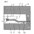
図1は、本実施形態1の半導体装置の外観(主面側)を示す平面図、
図2は、本実施形態1の半導体装置の外観(裏面側)を示す平面図(底面図)、
図3は、本実施形態1の半導体装置の内部構造(裏面側)を示す平面図、
図4は、図3の一部を拡大した断面図、
図5は、本実施形態1の半導体装置の内部構造を示す断面図((a)は図3のA−A線に沿う断面図,(b)は図3のB−B線に沿う断面図)、
図6は、図5(a)の一部を拡大した断面図である。
【0018】
図1乃至図5に示すように、本実施形態の半導体装置1aは、1つの半導体チップ2と、複数のリード4からなる第1及び第2のリード群と、複数のボンディングワイヤ7と、樹脂封止体8とを有するパッケージ構造になっている。半導体チップ2、第1及び第2のリード群の各リード4、並びに複数のボンディングワイヤ7等は樹脂封止体8で封止されている。
【0019】
半導体チップ2は、図3及び図5に示すように、厚さ方向と交差する平面形状が方形状になっており、本実施形態では例えば長方形になっている。半導体チップ2は、これに限定されないが、主に、半導体基板と、この半導体基板の主面に形成された複数のトランジスタ素子と、前記半導体基板の主面上において絶縁層、配線層の夫々を複数段積み重ねた多層配線層と、この多層配線層を覆うようしにて形成された表面保護膜(最終保護膜)とを有する構成になっている。絶縁層は、例えば酸化シリコン膜で形成されている。配線層は、例えばアルミニウム(Al)、又はアルミニウム合金、又は銅(Cu)、又は銅合金等の金属膜で形成されている。表面保護膜は、例えば、酸化シリコン膜又は窒化シリコン膜等の無機絶縁膜及び有機絶縁膜を積み重ねた多層膜で形成されている。
【0020】
半導体チップ2は、互いに反対側に位置する主面(回路形成面)2x及び裏面2yを有し、半導体チップ2の主面2x側には集積回路として例えばDRAM(DynamicRandomAccessMemory)からなる記憶回路が形成されている。この記憶回路は、主に、半導体基板の主面に形成されたトランジスタ素子及び多層配線層に形成された配線によって構成されている。
【0021】
半導体チップ2の主面2xには複数の電極2aが配置されている。複数の電極2aは、半導体チップ2の主面2aの2つの中心線のうちの一方の中心線(本実施形態では半導体チップ2の長辺方向と同一方向の中心線)に沿って配列された中央配列になっている。複数の電極パッド2aは、半導体チップ2の多層配線層のうちの最上層の配線層に形成され、半導体チップ2の表面保護膜に夫々の電極2aに対応して形成されたボンディング開口によって露出されている。
【0022】
樹脂封止体8は、図1、図2及び図5に示すように、厚さ方向と交差する平面形状が方形状になっており、本実施形態では例えば長方形になっている。樹脂封止体8は互いに反対側に位置する主面8x及び裏面(実装面)8yを有し、樹脂封止体8の平面サイズは半導体チップ2の平面サイズよりも大きくなっている。
【0023】
樹脂封止体8は、低応力化を図る目的として、例えば、フェノール系硬化剤、シリコーンゴム及びフィラー等が添加されたビフェニール系の樹脂で形成されている。この樹脂封止体8は、大量生産に好適なトランスファモールディング法で形成されている。トランスファモールデイング法は、ポット、ランナー、流入ゲート及びキャビティ等を備えたモールド金型を使用し、ポットからランナー及び流入ゲートを通してキャビティ内に樹脂を加圧注入して樹脂封止体を形成する方法である。本実施形態では、樹脂シートを用いて樹脂封止体8を形成するシートモールド技術を採用している。
【0024】
第1のリード群の各リード4は、図3乃至図5に示すように、半導体チップ2の互いに反対側に位置する2つの長辺のうちの一方の長辺に沿って配置され、第2のリード群の各リード4は、半導体チップ2の他方の長辺に沿って配置されている。半導体チップ2の一方の長辺は樹脂封止体8の互いに反対側に位置する2つの側面(8a,8b)のうちの一方の側面8bと同一側に位置し、半導体チップ2の他方の長辺は樹脂封止体8の他方の側面8aと同一側に位置している。
【0025】
第1のリード群の各リード4は、半導体チップ2の主面2xの外周辺を横切るようにして延在し、一端側が半導体チップ2に接着固定され、他端側が樹脂封止体8の一方の側面8a側に配置されている。第2のリード群の各リード4は、半導体チップ2の主面2xの外周辺を横切るようにして延在し、一端側が半導体チップ2に接着固定され、他端側が樹脂封止体8の他方の側面8b側に配置されている。本実施形態において、第1及び第2のリード群の各リード4の一端側は、複数の電極2aの配列方向に沿って配列され、樹脂からなる絶縁性テープ3を介在して半導体チップ2の主面2xに接着固定されている。また、第1及び第2ののリード群の各リード4の他端側は、樹脂封止体8の側面(8a,8b)の長手方向(半導体チップの長辺と同一方向)に沿って配列されている。
【0026】
半導体チップ2の複数の電極2aは、第1及び第2のリード群の各リード4に夫々電気的に接続されている。本実施形態において、半導体チップ2の電極2aとリード4との電気的な接続はボンディングワイヤ7で行われ、ボンディングワイヤ7の一端側は半導体チップ2の電極2aに接続され、ボンディングワイヤ7の他端側はリード4の一端側に接続されている。ボンディングワイヤ7としては、例えば金(Au)ワイヤを用いている。また、ワイヤ7の接続方法としては、例えば熱圧着に超音波振動を併用したネイルヘッドボンディング(ボールボンディング)法を用いている。
【0027】
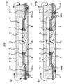
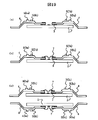
第1及び第2のリード群において、複数のリード4は、互いに隣り合う第1のリード4a及び第2のリード4bを含んでいる。第1のリード4aは、樹脂封止体8の裏面から露出し、かつ樹脂封止体8の側面側に位置する第1の外部接続部5aを有する構成になっている。第2のリード4bは、樹脂封止体8の裏面8yから露出し、かつ第1の外部接続部5aよりも半導体チップ2側、換言すれば、第1の外部接続部5aよりもリード4の一端側に位置する第2の外部接続部5bを有する構成となっている。第1のリード4a及び第2のリード4bは、樹脂封止体8の長手方向(半導体チップの長辺方向)に沿って交互に繰り返し配置されている。即ち、第1及び第2のリード群は、第1の外部接続部5aを有する第1のリード4a及び第2の外部接続部5bを有する第2のリード4bを一方向に交互に繰り返し配置した構成となっている。
【0028】
樹脂封止体8の裏面8yには、図2に示すように、複数の外部接続部5からなる第1及び第2の端子群が配置されている。第1の端子群の各外部接続部5は、樹脂封止体8の第1の側面8a側に樹脂封止体8の長手方向に沿って配置され、第2の端子群の各外部接続部5は、樹脂封止体8の第2の側面8b側に樹脂封止体8の長手方向に沿って配置されている。第1及び第2の端子群において、複数の外部接続部5は、樹脂封止体8の側面(8a,8b)側に位置する第1の外部接続部5aと、この第1の外部接続部5aよりも樹脂封止体8の側面から離れて位置する第2の外部接続部5bとを含み、第1及び第2の外部接続部(5a,5b)は樹脂封止体8の長手方(半導体チップの長辺方向)に沿って交互に繰り返し配置されている。即ち、第1及び第2の端子群は、第1の外部接続部5a及び第2の外部接続部5bを一方向に沿って繰り返し配置した千鳥配列になっている。
【0029】
複数のリード4(4a,4b)は、図6に示すように、半導体チップ2の主面2x上を延在する第1の部分4m1と、この第1の部分4m1から樹脂封止体8の裏面8y側に折れ曲がる第2の部分4m2と、この第2の部分4m2から樹脂封止体8の側面に向かって延びる第3の部分4m3とを有する構成になっている。
【0030】
第1及び第2の外部接続部(5a,5b)は、図3乃至図5に示すように、半導体チップ2の周囲において、第1及び第2のリード(4a,4b)の夫々の第3の部分4m3に設けられている。
【0031】
図5及び図6に示すように、外部接続部(5a,5b)5は、リード(4a,4b)と一体に形成されており、外部接続部5の厚さはリード4の第3の部分4m3の厚さよりも厚くなっている。本実施形態において、外部接続部5の厚さは例えば125μm〜150μm程度であり、外部接続部5以外のリード4の厚さ、即ち他の部分での厚さは例えば65μm〜75μm程度である。
【0032】
外部接続部5は、詳細に図示していないが、樹脂封止体8の裏面8yから外側に突出し、その先端部分は例えばメッキ法若しくは印刷法によって形成された半田層(メッキ層)9で覆われている。本実施形態の半導体装置1aは、これらの外部接続部5を配線基板の電極(フットプリント,ランド,パッド)に半田付けすることによって実装される。
【0033】
図4に示すように、外部接続部(5a,5b)5の幅5Wは、リード(4a,4b)4の第3の部分4m3の幅4Wよりも広くなっている。また、第1の外部接続部5aと第2の外部接続部5bとの間隔5Sは、第1のリード4aの第3の部分4m3と第2のリード4bの第3の部分4m3との間隔4Sよりも狭くなっている。また、樹脂封止体8の側面(8a,8b)から第2の外部接続部5bまでの距離L2は、樹脂封止体8の側面(8a,8b)から第1の外部接続部5aまでの距離L1よりも長くなっている。本実施形態において、幅5Wは例えば300μm程度であり、幅4Wは例えば200μm程度である。また、間隔5Sは例えば100μm程度であり、間隔4Sは例えば300μm程度である。また、距離L2は例えば0.8mm程度であり、距離L1は例えば0.1mm程度である。
【0034】
本実施形態の半導体装置1aは、樹脂封止体8の裏面8yから露出する複数の外部接続部5を樹脂封止体8の長手方向に沿って千鳥配列で配置したパッケージ構造になっている。このようなパッケージ構造にすることにより、実装時の信頼性を確保するために必要な外部接続部5の面積を確保してリード4の微細化を図ることができるため、パッケージサイズを変えずに多ピン化を図ることができる。
【0035】
次に、半導体装置1aの製造に使用されるリードフレームについて、図7乃至図9を用いて説明する。
【0036】
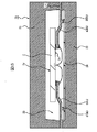
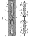
図7は、リードフレームの一部を示す平面図、
図8は、図7の一部を拡大した平面図、
図9は、リードフレームの一部を示す断面図((a)は第1のリードに沿う断面図,(b)は第2のリードに沿う断面図)である。
【0037】
図7に示すように、リードフレームLF1は、フレーム本体10で区画された複数の製品形成領域11をリードフレームLF1の長手方向に配置した多連構造になっている。各製品形成領域11には、図8及び図9に示すように、第1及び第2のリード(4a,4b)を含む複数のリード4からなる第1及び第2のリード群が配置されている。本実施形態において、製品形成領域11は長方形の平面形状になっている。第1及び第2のリード群は、製品形成領域11の短辺方向において、互いに向かい合い、かつ離間して配置されている。第1及び第2のリード群の各リード4は、製品形成領域11の長辺方向に沿って配置されている。第1及び第2のリード群において、互いに隣り合うリード4はタイバー12を介して連結されている。また、複数のリード4の夫々の一端側のボンディング面にはメッキ層6が設けられており、ボンディング面と反対側の面には製品形成領域11の長辺方向に沿って延在する絶縁性テープ3が貼り付けられている。また、複数のリード4の夫々の他端側はフレーム本体10に連結されている。
【0038】
リードフレームLF1を製造するには、まず、板厚が125μm〜150μm程度のCu、Cu合金、又はFe−Ni合金等からなる金属板を準備し、リード4を形成する箇所の片面をフォトレジスト膜で被覆する。また、外部接続部5を形成する箇所は、両面をフォトレジスト膜で被覆する。そして、この状態で金属板を薬液によってエッチングし、片面がフォトレジスト膜で被覆された領域の金属板の板厚を例えば半分程度(65μm〜75μm)まで薄くする(ハーフエッチング)。このような方法でエッチングを行うことにより、両面共にフォトレジスト膜で被覆されていない領域の金属板は完全に消失し、片面がフォトレジスト膜で被覆された領域に厚さ65μm〜75μm程度のリード4が形成される。また、両面がフォトレジスト膜で被覆された領域の金属板は薬液によってエッチングされないので、エッチング前と同じ厚さ(125μm〜150μm)を有する突起状の外部接続部5が形成される。次に、フォトレジスト膜を除去し、その後、リード4の一端側のボンディング面にメッキ層6を形成し、その後、リード4に折り曲げ加工を施すことによって、図7乃至図9に示すリードフレームLF1が完成する。
【0039】
次に、半導体装置1aの製造に用いられる成形金型について、図11乃至図14を用いて説明する。
【0040】
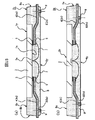
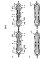
図11は、半導体装置1aの製造工程中のモールド工程において、第1のリードに沿う断面図、
図12は、図11の一部を拡大した断面図、
図13は、半導体装置1aの製造工程中のモールド工程において、第2のリードに沿う断面図、
図14は、図13の一部を拡大した断面図である。
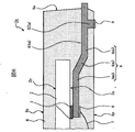
【0041】
図11乃至図14に示すように、成形金型20は、これに限定されないが、上下に分割された上型21及び下型22を有し、更に、ポット、カル部、ランナー、樹脂注入ゲート、キャビティ23、エアーベント等を有する構成となっている。上型21は、第1の合わせ面に、第1のクランプ部21aと、この第1のクランプ部21aに連なるキャビティ23と、このキャビティ23に樹脂注入ゲートを介して一端側が連なるランナーと、このランナーの他端側に連なるカル部と、このカル部に連なるポット部と、キャビティ23に連なるエアーベントとを有し、下型22は、第1の合わせ面と向かい合う第2の合わせ面に、第1のクランプ部と向かい合う第2のクランプ部22aを有する構成になっている。キャビティ23は、上型21の第1のクランプ部21aから上型21の深さ方向に窪んだ構成になっている。キャビティ23の平面形状は方形状になっており、本実施形態では長方形になっている。
【0042】
シートモールド技術による樹脂封止体の形成では、成形金型20の下型22とリードフレームLF1との間に樹脂シート(樹脂フィルム)24が位置するように、成形金型20の上型21と下型22との間にリードフレームLF1を位置決めし、その後、ポットからカル部、ランナー及び樹脂注入ゲートを通してキャビティ23の内部に樹脂を加圧注入することによって行われる。シートモールド技術では、一般的に熱硬化性の樹脂が用いられるため、樹脂シート24としては樹脂封止体形成時の温度に耐える耐熱性の樹脂シートを用いる。また、スタンドオフ・パッケージ構造にするには、成形金型20のクランプ力(締め付け力)によってリード4の外部接続部5を樹脂シート24に食い込ませる必要があるため、成形金型20のクランプ力で容易に潰すことが可能な柔軟性のある樹脂シート(可撓性樹脂シート)24を用いる。
【0043】
次に、半導体装置1aの製造について、図10乃至図14を用いて説明する。
【0044】
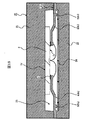
図10は、半導体装置1aの製造工程中における断面図((a)はダイボンディング工程での断面図,(b)はワイヤボンディング工程での断面図)である。
【0045】
まず、図7乃至図9に示すリードフレームLF1を準備し、その後、図10(a)に示すように、リードフレームLF1に半導体チップ2を接着固定する。リードフレームLF1と半導体チップ2との接着固定は、絶縁性テープ3を介在して、半導体チップ2の主面2xにリード4の一端側(第1の部分4m1)を接着固定することによって行われる。
【0046】
次に、図10(b)に示すように、半導体チップ2の主面2xに配置された複数の電極2aと複数のリード4とを複数のボンディングワイヤ7で夫々電気的に接続する。ボンディングワイヤ7の一端側は、半導体チップ2の電極2aに接続され、他端側はリード4の一端側のボンディング面に設けられたメッキ層6に接続される。
【0047】
次に、図11乃至図14に示す成形金型20を準備し、その後、同図に示すように、成形金型20の上型21と下型22との間にリードフレームLF1を位置決めする。
【0048】
リードフレームLF1の位置決めは、リードフレームLF1と下型22の合わせ面との間に樹脂シート24が介在する状態で行われる。
また、リードフレームLF1の位置決めは、キャビティ23の内部に、半導体チップ2、ボンディングワイヤ7等が位置する状態で行われる。
【0049】
また、リードフレームLF1の位置決めは、リード(4a,4b)4の他端側を上型21の第1のクランプ部21a及び下型22の第2のクランプ部22aで上下方向から挟み込み、リード(4a,4b)4と下型22の第2の合わせ面との間に配置された樹脂シート24に外部接続部(5a,5b)5を接触させた状態で行われる。
【0050】
次に、前述のようにリードフレームLF1を位置決めした状態で、成形金型20のポットからカル部、ランナー及び樹脂注入ゲートを通してキャビティ23の内部に例えば熱硬化性の樹脂を加圧注入して樹脂封止体8を形成する。半導体チップ2、複数のリード4、複数のボンディングワイヤ7等は、樹脂封止体8によって封止される。
【0051】
この工程において、樹脂封止体8の裏面8yから外部接続部5が露出し、かつ樹脂封止体8の裏面8yから外側に外部接続部5が突出するスタンドオフ・パッケージがほぼ完成する。
【0052】
次に、リードフレームLF1に貼り付いた樹脂シート24を剥がして成形金型20からリードフレームLF1を取り出し、その後、樹脂封止体8の硬化を促進するキュア工程を施した後、タイバー12を分離する切断工程、フレーム本体10からリード4を分離する切断工程等をほどこすことにより、本実施形態の半導体装置1aがほぼ完成する。
【0053】
本実施形態の半導体装置の製造工程中におけるモールド工程では、リードフレームLF1と成形金型20の下型22との間に樹脂シート24を配置したシートモールド技術を採用し、樹脂シート24にリード4の外部接続部5を接触させた状態でリード4の他端側を上型21のクランプ部21aと下型22のクランプ部22aとで上下方向から挟み込んでいる。このようにすると、リード4の外部接続部5が成型金型20(上型21及び下型22)の押圧力によって樹脂シート24を押さえ付けるため、外部接続部5の先端部が樹脂シート24に食い込む。この結果、キャビティ23の内部に樹脂を注入して樹脂封止体8を形成した後、成型金型20からリードフレームLF1を取り出すと、樹脂シート24に食い込んでいた外部接続部5の先端部が樹脂封止体8の裏面8yから外部に突出する。
【0054】
また、成型金型20のクランプ力によってリードフレームLF1を押さえ付けると、リードフレームLF1を構成する金属板のバネ力によって、リード4の先端側である一端側に上向きの力が作用する。そのため、本実施形態のように、複数の外部接続部5を千鳥配列にした場合は、リード4の他端側に近い位置に外部接続部5(5a)が形成されたリード4(4a)と、外部接続部5aよりもリード4の他端側から遠い位置に外部接続部5(5b)が形成されたリード4(4b)とでは、外部接続部5が樹脂シート24を押さえ付ける力に差が生じる。即ち、リード4bに形成された外部接続部5bは、リード4aに形成された外部接続部5aに比べて樹脂シート24を押さえる力が弱くなる。この結果、成形金型20のクランプ部から外部接続部5aよりも遠い外部接続部5bは、樹脂シート24との密着性が低下し、外部接続部5bがレジンバリによって覆われてしまうといった不具合が発生し易くなる。
【0055】
これに対し、本実施形態では、リード4の一端側を半導体チップ2の主面2xに接着固定した状態で樹脂封止している。このような状態で樹脂封止することにより、成型金型20のクランプ力によってリードフレームLF1を押さえ付けることによって生じるリード4の反りを抑制できるため、樹脂シート24を押さえる外部接続部5bの押さえ力の低下を抑制できる。従って、成型金型20のクランプ部から遠い外部接続部5bと樹脂シート24との密着性を確保できるため、外部接続部5bがレジンバリによって覆われてしまうといった不具合の発生を抑制できる。この結果、半導体装置1aの製造歩留まりの向上を図ることができる。
【0056】
(実施形態2)
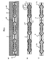
図15は、本実施形態2の半導体装置の断面図((a)は第1のリードに沿う断面図,(b)は第2のリードに沿う断面図)、
図16は、本実施形態2の半導体装置の製造工程中のモールド工程において、第1のリードに沿う断面図、
図17は、本実施形態2の半導体装置の製造工程中のモールド工程において、第2のリードに沿う断面図である。
【0057】
図15に示すように、本実施形態2の半導体装置1bは、基本的に前述の実施形態1と同様の構成になっており、以下の構成が異なっている。
【0058】
即ち、前述の実施形態1の半導体装置1aでは、半導体チップ2の裏面2yが樹脂封止体8の樹脂で覆われたパッケージ構造になっているが、本実施形態2の半導体装置1bでは、半導体チップ2の裏面2yが樹脂封止体8の主面8xから露出するパッケージ構造、換言すれば、半導体チップ2の裏面2yが樹脂封止体8の樹脂で覆われないパッケージ構造になっている。
【0059】
このようなパッケージ構造は、モールド工程において、図16及び図17に示すように、半導体チップ2の裏面2yをこの裏面2yと向かい合うキャビティ23の内壁面に接触させた状態で樹脂封止することで得られる。
【0060】
このようなパッケージ構造においても、前述の実施形態と同様の効果が得られる。
【0061】
また、本実施形態では、リード4の一端側を半導体チップ2の主面2xに接着固定させ、半導体チップ2の裏面2yをキャビティ23の内壁面に接触させた状態で樹脂封止している。このような状態で樹脂封止することにより、成型金型20のクランプ力でリードフレームLF1を押さえ付けることによって生じるリード4の反りを更に抑制できるため、外部接続部5bがレジンバリによって覆われてしまうといった不具合の発生を更に抑制できる。
【0062】
(実施形態3)
図18は、本実施形態3の半導体装置の断面図((a)は第1のリードに沿う断面図,(b)は第2のリードに沿う断面図)である。
【0063】
図18に示すように、本実施形態3の半導体装置1cは、基本的に前述の実施形態1と同様の構成になっており、以下の構成が異なっている。
【0064】
即ち、前述の実施形態1の半導体装置1aでは、半導体チップ2の主面2xが樹脂封止体8の裏面8y側に位置するパッケージ構造、換言すれば半導体チップ2の裏面2yと樹脂封止体8の裏面8yとが同一側に位置するパッケージ構造になっているが、本実施形態3の半導体装置1bでは、半導体チップ2の裏面2yが樹脂封止体8の裏面8y側に位置するパッケージ構造、換言すれば半導体チップ2の裏面2yと樹脂封止体8の裏面8yとが同一側に位置するパッケージ構造になっている。このような半導体装置1cにおいても、前述の実施形態1と同様の効果が得られる。
【0065】
(実施形態4)
本実施形態4は、2つの半導体チップを1つの樹脂封止体で封止した半導体装置に本発明を適用した例である。
【0066】
図19及び図20は、本実施形態の半導体装置の製造工程を示す断面図((a),(b),(c))である。
【0067】
本実施形態の半導体装置1dは、図20(d)に示すように、同一構造の2つの半導体チップ2をその裏面同士が向かい合う状態で積層し、この2つの半導体チップ2を1つの樹脂封止体8で封止したパッケージ構造になっている。本実施形態の半導体装置1dは、同一のリードパターンを有する2枚のリードフレームを重ね合わせて製造されるため、2つの半導体チップ2の合わせ面を境にして上側の構造及び下側の構造がほぼ対称になっている。
【0068】
一方の半導体チップ2(図中、上側)の互いに反対側に位置する2つの長辺のうちの一方の長辺側には、その一方の長辺に沿って複数のリード4が配置され、他方の長辺側においてもその他方の長辺に沿って複数のリード4が配置されている。一方の長辺側の複数のリード4は、一端側が絶縁性テープ3を介在して一方の半導体チップ2の主面に接着固定され、他端側が樹脂封止体8の側面8a側に配置されている。他方の長辺側の複数のリード4は、一端側が絶縁性テープ3を介在して一方の半導体チップ2の主面に接着固定され、他端側が樹脂封止体8の側面8b側に配置されている。
【0069】
他方の半導体チップ2(図中、下側)の互いに反対側に位置する2つの長辺のうちの一方の長辺側には、その一方の長辺に沿って複数のリード4が配置され、他方の長辺側においてもその他方の長辺に沿って複数のリード4が配置されている。一方の長辺側の複数のリード4は、一端側が絶縁性テープ3を介在して一方の半導体チップ2の主面に接着固定され、他端側が樹脂封止体8の側面8a側に配置されている。他方の長辺側の複数のリード4は、一端側が絶縁性テープ3を介在して他方の半導体チップ2の主面に接着固定され、他端側が樹脂封止体8の側面8b側に配置されている。
【0070】
樹脂封止体8の主面には複数の外部接続部5が配置されている。また、樹脂封止体8の裏面においても複数の外部接続部5が配置されている。これらの外部接続部5は、前述の実施形態1と同様の千鳥配列になっている。従って、本実施形態の半導体装置1dは、樹脂封止体8の主面又は裏面を実装面として配線基板に実装することができる。また、同一の2つの半導体装置1dを上下方向に積み重ねて実装することもできる。
【0071】
本実施形態のリード4は、前述の実施形態1のリード4と比較して形状が異なっている。実施形態1のリード4は2つの折り曲げ箇所を有する形状になっているが、本実施形態のリード4は4つの折り曲げ箇所を有する形状になっている。従って、本実施形態のリード4は、半導体チップ2の主面上を延在する第1の部分と、この第1の部分から樹脂封止体8の実装面(主面又は裏面)側に折れ曲がる第2の部分と、この第2の部分から樹脂封止体8の側面に向かって延びる第3の部分と、この第3の部分から半導体チップ2側に折れ曲がる第4の部分と、この第4の部分から樹脂封止体8の側面に向かって延びる第5の部分とを有する構成になっている。外部接続部5は、実施形態1と同様に、第3の部分に設けられている。
【0072】
上側のリード4の第5の部分は、対応する下側のリード4の第5の部分に電気的にかつ機械的に接続されている。
【0073】
次に、半導体装置1dの製造について、図19及び図20を用いて説明する。
【0074】
まず、同一のリードパターンを有する2枚のリードフレームを準備し、一方及び他方のリードフレームに半導体チップ2を接着固定する。リードフレームと半導体チップ2との接着固定は、図19(a)に示すように、絶縁性テープ3を介在して半導体チップ2の主面にリード4の一端側を接着固定することによって行われる。
【0075】
次に、一方及び他方のリードフレームにおいて、図19(b)に示すように、半導体チップ2の電極とリード4とをボンディングワイヤ7で電気的に接続する。一方のリードフレームのリード4と半導体チップ2の電極との接続は、他方のリードフレームのリード4と半導体チップ2の電極との接続に対してワイヤ7の引き回しが左右逆になるように逆ボンディングで行う。
【0076】
次に、図19(c)及び図20(a)に示すように、一方のリードフレームの半導体チップ2と他方のリードフレームの半導体チップ2の裏面同士を向かい合わせた状態で、一方及び他方のリードフレームを重ね合わせ、その後、一方のリードフレームのリード4の第5の部分と他方のリードフレームのリード4の第5の部分とを電気的にかつ機械的に接続する。このリード4の接続は、例えばレーザ溶接にて行う。
【0077】
次に、図20(b)に示すように、2つの半導体チップ2、一方及び他方のリードフレームのリード4、並びにボンディングワイヤ7等を樹脂で封止して樹脂封止体8を形成する。この樹脂封止体8の形成は、実施形態1と同様のシートモールド技術を用いて行う。但し、本実施形態の場合は、成形金型の下型とリードフレームとの間、及び成形金型の上型とリードフレームとの間に樹脂シートを介在して行う。これにより、樹脂封止体8の主面及びその裏面に千鳥状に複数の外部接続部5が配置されたパッケージが形成される。
【0078】
次に、リードフレームに貼り付いた樹脂シートを剥がして成形金型からリードフレームを取り出し、その後、図20(c)に示すように、樹脂封止体8から露出する外部接続部5の先端部に半田層9を形成し、その後、樹脂封止体8の硬化を促進するキュア工程を施した後、2枚のリードフレームのタイバーを分離する切断工程、フレーム本体からリード4を分離する切断工程等をほどこすことにより、本実施形態の半導体装置1dがほぼ完成する。
【0079】
このように、本実施形態の半導体装置1dは、1つの樹脂封止体8で2つの半導体チップ2を封止したパッケージ構造になっているので、高密度実装が可能となる。
【0080】
また、本実施形態の半導体装置1dは、樹脂封止体8の主面及びその裏面に千鳥状に複数の外部接続部5が配置されたパッケージ構造になっているので、樹脂封止体8の主面又は裏面を実装面として配線基板に実装することができる。また、同一の2つの半導体装置1dを上下方向に積み重ねて実装することもできるので、更に高密度実装が可能となる。
【0081】
(実施形態5)
本実施形態5は、2つの半導体チップを積層した半導体装置をスルーモールド方式で製造する例である。
【0082】
図21乃至図23は、本実施形態5の半導体装置の製造工程を示す断面図((a),(b))である。
【0083】
まず、同一のリードパターンを有する多連構造の2枚のリードフレームを準備し、その後、実施形態4と同様のダイボンディング工程、ワイヤボンディング工程を施し、その後、図21(a)に示すように、一方のリードフレームの半導体チップ2と他方のリードフレームの半導体チップ2の裏面同士を向かい合わせた状態で、一方及び他方のリードフレームを重ね合わせる。
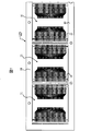
【0084】
次に、図21(b)に示すように、重ね合わせた2枚のリードフレームと成形金型30の上型31との間、重ね合わせた2枚のリードフレームと成形金型30の下型32との間に夫々樹脂シート24を介在して、重ね合わせた2枚のリードフレームを成形金型30の上型31と下型32との間に位置決めする。本実施形態の2枚のリードフレームは、複数の製品形成領域を行列状に配置している。従って、成形金型30においても、リードフレームの製品形成領域に対応して複数のキャビティ33を行列状に配置している。成形金型30においては、複数のキャビティからなる列毎に樹脂注入ゲート34が設けられ、樹脂注入ゲート34は、各列の初段のキャビティ33に連結されている。各列の隣り合うキャビティ33は、スルーゲート35(図22(a)参照)で連結されている。
【0085】
次に、成形金型30のポットからランナー、樹脂注入ゲート34等を通してキャビティ33の内部に樹脂を加圧注入して、図22(a)に示すように、2つの半導体チップ2、一方及び他方のリードフレームのリード4、並びにボンディングワイヤ7等を樹脂で封止して樹脂封止体8を形成する。
【0086】
次に、図22(b)に示すように、成形金型30から2枚のリードフレームを取り出し、その後、一方のリードフレームのリード4の第5の部分と他方のリードフレームのリード4の第5の部分とを電気的にかつ機械的に接続する。このリード4の接続は、例えばレーザ溶接にて行う。
【0087】
次に、図23(a)に示すように、樹脂封止体8から露出する外部接続部5の先端部に半田層9を形成し、その後、樹脂封止体8の硬化を促進するキュア工程を施した後、2枚のリードフレームのタイバーを分離する切断工程、フレーム本体からリード4を分離する切断工程等をほどこすことにより、図23(b)に示す本実施形態の半導体装置1eがほぼ完成する。
【0088】
このように、本実施形態においても、前述の実施形態4と同様の効果が得られる。
【0089】
(実施形態6)
本実施形態6は、2つの半導体チップを積層した半導体装置を一括モールド方式で製造する例である。
【0090】
図24乃至図25は、本実施形態の半導体装置の製造工程を示す断面図((a),(b),(c))、
図26は、本実施形態の半導体装置の内部構造を示す断面図である。
【0091】
本実施形態6の半導体装置1gは、樹脂封止体8の主面と裏面の平面サイズがほぼ同一となっており、樹脂封止体8の側面はその主面及び裏面に対してほぼ垂直になっている。本実施形態の半導体装置1gの製造においては、一括モールド方式が採用されている。従って、半導体装置1gは、後で詳細に説明するが、リードフレームの複数の製品形成領域に夫々搭載された半導体チップを一括して1つの樹脂封止体で封止した後、リードフレーム及び樹脂封止体を製品形成領域毎に分割することによって製造される。
【0092】
本実施形態の半導体装置1gの製造について、図24及び図25を用いて説明する。
【0093】
まず、同一のリードパターンを有する多連構造の2枚のリードフレームを準備し、その後、実施形態4と同様のダイボンディング工程、ワイヤボンディング工程を施し、その後、図24(a)に示すように、一方のリードフレームの半導体チップ2と他方のリードフレームの半導体チップ2の裏面同士を向かい合わせた状態で、一方及び他方のリードフレームを重ね合わせる。この時、半田材又は導電性の接着材を用いて、一方のリードフレームのリード4の第5の部分と他方のリードフレームのリード4の第5の部分とを電気的にかつ機械的に接続する。
【0094】
次に、図24(b)に示すように、重ね合わせた2枚のリードフレームと成形金型40の上型41との間、重ね合わせた2枚のリードフレームと成形金型40の下型42との間に夫々樹脂シート24を介在して、重ね合わせた2枚のリードフレームを成形金型30の上型31と下型32との間に位置決めする。本実施形態の2枚のリードフレームは、複数の製品形成領域を行列状に配置している。本実施形態の成形金型40は、リードフレームの複数の製品形成領域を一括して配置できるキャビティ43を備えている。
【0095】
次に、成形金型40のポットからランナー、樹脂注入ゲート44等を通してキャビティ43の内部に樹脂を加圧注入して、図25(a)に示すように、2つの半導体チップ2、一方及び他方のリードフレームのリード4、並びにボンディングワイヤ7等を樹脂で封止して樹脂封止体8を形成する。
【0096】
次に、成形金型40から2枚のリードフレームを取り出し、その後、図25(b)に示すように、樹脂封止体8から露出する外部接続部5の先端部に半田層9を形成し、その後、図25(c)に示すように、2枚のリードフレーム及び樹脂封止体8を製品形成領域毎に分割することにより、本実施形態の半導体装置1gがほぼ完成する。
【0097】
このように、本実施形態においても、前述の実施形態4と同様の効果が得られる。
【0098】
(実施形態7)
図27は、本実施形態の半導体装置の内部構造を示す断面図である。
【0099】
図27に示すように、本実施形態の半導体装置1hは、基本的に前述の実施形態6と同様の構成になっており、以下の構成がことなっている。
【0100】
即ち、実施形態6の半導体装置1hは、樹脂封止体8の主面及びその裏面に千鳥状に複数の外部接続部5が配置されたパッケージ構造になっているが、本実施形態の半導体装置1hは、樹脂封止体8の裏面側のみ、複数の外部接続部5が千鳥状に配置されたパッケージ構造になっている。このようなパッケージ構造の半導体装置1hは、2枚のリードフレームのうち一方のリードフレームとして、リード4に外部接続部5を持たないリードフレームを用し、一括モールド方式によって製造する。本実施形態の半導体装置1hにおいても、実施形態1と同様の効果が得られる。
【0101】
(実施形態8)
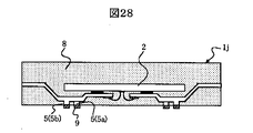
図28は、本実施形態の半導体装置の内部構造を示す断面図である。
【0102】
本実施形態の半導体装置1jは、1つの半導体チップ2を1つの樹脂封止体8で封止したパッケージ構造になっている。本実施形態の半導体装置1jは、1枚のリードフレームを用い、一括モールド方式によって製造する。本実施形態の半導体装置1jにおいても、実施形態1と同様の効果が得られる。
【0103】
(実施形態9)
図29は、本実施形態の半導体装置の内部構造を示す断面図である。
【0104】
本実施形態の半導体装置1kは、異なる構造の2つの半導体チップ(2,50)をその裏面同士が向かい合う状態で積層し、この2つの半導体チップを1つの樹脂封止体8で封止したパッケージ構造になっており、さらに、樹脂封止体8の裏面側のみ、複数の外部接続部5が千鳥状に配置されたパッケージ構造になっている。半導体チップ50の電極は、リード4と形状が異なるリード51にボンディングワイヤを介して電気的に接続され、リード51は、リード4の第5の部分に電気的にかつ機械的に接続されている。本実施形態においても、高密度実装が可能となる。
【0105】
(実施形態10)
図30は、本実施形態の半導体装置の内部構造を示す断面図である。
【0106】
図30に示すように、本実施形態の半導体装置1mは、基本的に実施形態9と同様の構成になっており、以下の構成が異なっている。
【0107】
即ち、半導体チップ50は、半導体チップ50と半導体チップ2との間に引き伸ばされたリード51に絶縁性接着材を介在して接着固定されている。本実施形態においても、高密度実装が可能となる。
【0108】
(実施形態11)
図31は、本実施形態の半導体装置の内部構造を示す断面図である。
【0109】
図31に示すように、本実施形態の半導体装置1nは、基本的に実施形態9と同様の構成になっており、以下の構成が異なっている。
【0110】
即ち、半導体チップ50の主面に配置された電極とリード51とは、これらの間に介在された導電性のバンプ52によって電気的にかつ機械的に接続されている。本実施形態においても、高密度実装が可能となる。
【0111】
(実施形態12)
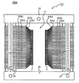
図32は、本実施形態のモジュールの概略構成を示す断面図、
図33は、本実施形態のモジュールの製造において、半導体装置を実装する第1の実装方法を示す断面図、
図34及び図35は、本実施形態のモジュールの製造において、半導体装置を実装する第2の実装方法を示す断面図である。
【0112】
本実施形態のモジュール(電子装置)は、2つの半導体装置1gを上下に積み重ねた状態で配線基板53に実装している。下段の半導体装置1gは、樹脂封止体8の裏面の外部接続部5が配線基板53の電極54に半田層9を介在して電気的にかつ機械的に接続され、樹脂封止体8の主面の外部接続部5が上段の半導体装置1gの樹脂封止体8の裏面に配置された外部接続部5に半田層9を介在して電気的にかつ機械的に接続されている。
【0113】
2つの半導体装置1gは、モジュールの製造において実装される。2つの半導体装置1gの実装方法としては、以下に示す2つの方法がある。
【0114】
第1の実装方法:
図33に示すように、2つの半導体装置1gを上下に積み重ねて配線基板53上に配置し、その後、半田層9を溶融して実装する。この場合、下側の半導体装置1gの裏面側及び主面側の半田層9、及び上側の半導体装置1gの裏面側の半田層9としては、融点が同じ材料のものを用いる。
【0115】
第2の実装方法:
図34に示すように、下側の半導体装置1gを先に実装し、その後、図35に示すように、下側半導体装置1g上に上側の半導体装置1gを実装する。この場合、下側の半導体装置1gの主面側の半田層9、及び上側の半導体装置1gの裏面側の半田層9としては、下側の半導体装置1gの裏面側の半田層9よりも融点が高い材料のものを用いる。
【0116】
このように、半導体装置1gは、樹脂封止体8の主面及びその裏面に千鳥状に複数の外部接続部5が配置されたパッケージ構造になっているため、同一の2つの半導体装置1gを上下方向に積み重ねて実装することができ、モジュールの高密度実装化を図ることができる。
【0117】
なお、本実施形態では同一の2つの半導体装置1gを積み重ねた例について説明したが、2つの半導体装置を積層する場合は、上側の半導体装置として、図27に示す半導体装置1h又は図28に示す半導体装置1jを用いてもよい。
【0118】
以上、本発明者によってなされた発明を、前記実施の形態に基づき具体的に説明したが、本発明は、前記実施の形態に限定されるものではなく、その要旨を逸脱しない範囲において種々変更可能であることは勿論である。
【0119】
【発明の効果】
本願において開示される発明のうち代表的なものによって得られる効果を簡単に説明すれば、下記のとおりである。
【0120】
本発明によれば、多ピン化に適した半導体装置の製造歩留まりの向上を図ることが可能となる。
【図面の簡単な説明】
【図1】本発明の実施形態1である半導体装置の外観(主面側)を示す平面図である。
【図2】本発明の実施形態1である半導体装置の外観(裏面側)を示す平面図(底面図)である。
【図3】本発明の実施形態1である半導体装置の内部構造(裏面側)を示す平面図である。
【図4】図3の一部を拡大した断面図である。
【図5】本発明の実施形態1である半導体装置の内部構造を示す断面図((a)は図3のA−A線に沿う断面図,(b)は図3のB−B線に沿う断面図)である。
【図6】図5(a)の一部を拡大した断面図である。
【図7】本発明の実施形態1である半導体装置の製造において使用されるリードフレーの一部を示す平面図である。
【図8】図7の一部を拡大した平面図である。
【図9】本発明の実施形態1である半導体装置の製造において使用されるリードフレームの一部を示す断面図((a)は第1のリードに沿う断面図,(b)は第2のリードに沿う断面図)である。
【図10】本発明の実施形態1である半導体装置の製造工程中における断面図((a)はダイボンディング工程での断面図,(b)はワイヤボンディング工程での断面図)である。
【図11】本発明の実施形態1である半導体装置の製造工程中のモールド工程において、第1のリードに沿う断面図である。
【図12】図11の一部を拡大した断面図である。
【図13】本発明の実施形態1である半導体装置の製造工程中のモールド工程において、第2のリードに沿う断面図である。
【図14】図13の一部を拡大した断面図である。
【図15】本発明の実施形態2である半導体装置の断面図((a)は第1のリードに沿う断面図,(b)は第2のリードに沿う断面図)である。
【図16】本発明の実施形態2である半導体装置の製造工程中のモールド工程において、第1のリードに沿う断面図である。
【図17】本発明の実施形態2である半導体装置の製造工程中のモールド工程において、第2のリードに沿う断面図である。
【図18】本発明の実施形態3である半導体装置の断面図((a)は第1のリードに沿う断面図,(b)は第2のリードに沿う断面図)である。
【図19】本発明の実施形態4である半導体装置の製造工程を示す断面図((a),(b),(c))である。
【図20】本発明の実施形態4である半導体装置の製造工程を示す断面図((a),(b),(c))である。
【図21】本発明の実施形態5である半導体装置の製造工程を示す断面図((a),(b))である。
【図22】本発明の実施形態5である半導体装置の製造工程を示す断面図((a),(b))である。
【図23】本発明の実施形態5である半導体装置の製造工程を示す断面図((a),(b))である。
【図24】本発明の実施形態6である半導体装置の製造工程を示す断面図((a),(b))である。
【図25】本発明の実施形態6である半導体装置の製造工程を示す断面図((a),(b),(c))である。
【図26】本発明の実施形態6である半導体装置の内部構造を示す断面図である。
【図27】本発明の実施形態7である半導体装置の内部構造を示す断面図である。
【図28】本発明の実施形態8である半導体装置の内部構造を示す断面図である。
【図29】本発明の実施形態9である半導体装置の内部構造を示す断面図である。
【図30】本発明の実施形態10である半導体装置の内部構造を示す断面図である。
【図31】本発明の実施形態11である半導体装置の内部構造を示す断面図である。
【図32】本発明の実施形態12であるモジュールの概略構成を示す断面図である。
【図33】本発明の実施形態12であるモジュールの製造において、半導体装置の第1の実装方法を示す断面図である。
【図34】本発明の実施形態12であるモジュールの製造において、半導体装置の第2の実装方法を示す断面図である。
【図35】本発明の実施形態12であるモジュールの製造において、半導体装置の第2の実装方法を示す断面図である。
【符号の説明】
1a,1b,1c,1d,1f,1g,1h,1j,1k,1m,1n…半導体装置、2…半導体チップ、2x…主面(回路形成面,)、2y…裏面、3…絶縁性テープ(絶縁性フィルム)、4…リード、4a…第1のリード、4b…第2のリード、5…外部接続部(外部端子部)、5a…第1の外部接続部、5b…第2の外部接続部、6…メッキ層、7…ボンディングワイヤ、8…樹脂封止体、8a,8b…側面、8x…主面、8y…裏面(実装面)、9…半田層(メッキ層)、LF1…リードフレーム、10…フレーム本体、11…製品形成領域、12…タイバー、20…成形金型、21…上型、21a…第1のクランプ部、22…下型、22a…第2のクランプ部、23…キャビティ、24…樹脂シート。
Claims (32)
- 主面に複数の電極が配置された半導体チップと、
前記半導体チップの複数の電極に夫々電気的に接続された複数のリードと、
前記半導体チップ及び前記複数のリードを封止する樹脂封止体とを有し、
前記複数のリードは、前記樹脂封止体の実装面から露出し、かつ前記樹脂封止体の側面側に位置する第1の外部接続部を有する第1のリードと、前記第1のリードと隣り合う第2のリードであって、前記樹脂封止体の実装面から露出し、かつ前記第1の外部接続部よりも前記半導体チップ側に位置する第2の外部接続部を有する第2のリードとを含み、
前記第1及び第2のリードは、前記半導体チップに接着固定されていることを特徴とする半導体装置。 - 請求項1に記載の半導体装置において、
前記第1及び第2のリードは、一端側が前記半導体チップの主面に接着固定され、前記一端側とは反対側の他端側が前記樹脂封止体の側面側に配置されていることを特徴とする半導体装置。 - 請求項1に記載の半導体装置において、
前記第1及び第2のリードは、半導体チップの外周の辺を横切って延在し、
前記第1及び第2の外部接続部は、前記半導体チップの周囲における前記第1及び第2のリードの部分に設けられていることを特徴とする半導体装置。 - 請求項1に記載の半導体装置において、
前記第1及び第2のリードは、前記半導体チップの主面上を延在する第1の部分と、前記第1の部分から前記樹脂封止体の実装面側に折れ曲がる第2の部分と、前記第2の部分から前記樹脂封止体の側面に向かって延びる第3の部分とを有し、
前記第1及び第2の外部接続部は、前記第1及び第2のリードの夫々の第3の部分に設けられていることを特徴とする半導体装置。 - 請求項4に記載の半導体装置において、
前記第1及び第2のリードの夫々の第1の部分は、半導体チップの主面に接着固定されていることを特徴とする半導体装置。 - 請求項1に記載の半導体装置において、
前記半導体チップの主面は、前記樹脂封止体の実装面側に位置していることを特徴とする半導体装置。 - 請求項1に記載の半導体装置において、
前記半導体チップの主面と反対側の裏面は、前記樹脂封止体から露出していることを特徴とする半導体装置。 - 請求項1に記載の半導体装置において、
前記半導体チップの主面と反対側に裏面は、樹脂封止体の実装面側に位置していることを特徴とする半導体装置。 - 請求項4に記載の半導体装置において、
前記第1及び第2の外部接続部の幅は、前記第1及び第2のリードの第3の分部の幅よりも広くなっていることを特徴とする半導体装置。 - 請求項4に記載の半導体装置において、
前記第1及び第2の外部接続部の間隔は、前記第1及び第2のリードの第3の部分の間隔よりも狭くなっていることを特徴とする半導体装置。 - 請求項1に記載の半導体装置において、
前記第1及び第2の外部接続部の厚さは、前記第1及び第2のリードの厚さよりも厚くなっていることを特徴とする半導体装置。 - 請求項1に記載の半導体装置において、
前記第1及び第2の外部接続部は、前記樹脂封止体の実装面から突出していることを特徴とする半導体装置。 - 請求項1に記載の半導体装置において、
前記複数のリードは、ボンディングワイヤを介して前記半導体チップの複数の電極と夫々電気的に接続されていることを特徴とする半導体装置。 - 請求項1に記載の半導体装置において、
前記半導体チップは、その厚さ方向と交差する平面形状が方形状で形成され、
前記複数の電極は、前記半導体チップの主面の2つの中心線のうちの一方の中心線に沿う中央配列になっていることを特徴とする半導体装置。 - 請求項1に記載の半導体装置において、
前記半導体チップは、その厚さ方向と交差する平面形状が長方形で形成され、
前記複数の電極は、前記半導体チップの主面の長辺方向と同一方向の中心線に沿う中央配列になっていることを特徴とする半導体装置。 - 請求項1に記載の半導体装置において、
前記第1及び第2のリードは、絶縁性テープを介在して前記半導体チップに接着固定されていることを特徴とする半導体装置。 - 主面に複数の電極が配置された半導体チップと、
前記半導体チップの第1の辺に沿って配置され、かつ前記半導体チップの複数の電極に夫々電気的に接続された複数のリードからなる第1のリード群と、
前記半導体チップの第1の辺と反対側の第2の辺に沿って配置され、かつ前記半導体チップの複数の電極に夫々電気的に接続された複数のリードからなる第2のリード群と、
前記半導体チップ、前記第1及び第2のリード群を封止する樹脂封止体とを有し、
前記第1及び第2のリード群は、前記樹脂封止体の実装面から露出し、かつ前記樹脂封止体の側面側に位置する第1の外部接続部を有する第1のリードと、前記第1のリードと隣り合う第2のリードであって、前記樹脂封止体の実装面から露出し、かつ前記第1の外部接続部よりも前記半導体チップ側に位置する第2の外部接続部を有する第2のリードとを含み、
前記第1及び第2のリードは、前記半導体チップに接着固定されていることを特徴とする半導体装置。 - 請求項17に記載の半導体装置において、
前記第1のリード群の第1及び第2のリードは、一端側が前記半導体チップの主面に接着固定され、前記一端側とは反対側の他端側が前記樹脂封止体の第1の側面側に配置され、
前記第2のリード群の第1及び第2のリードは、一端側が前記半導体チップの主面に接着固定され、前記一端側とは反対側の他端側が前記樹脂封止体の第1の側面とは反対側の第2の側面側に配置されていることを特徴とする半導体装置。 - 請求項17に記載の半導体装置において、
前記第1及び第2のリードは、前記半導体チップの主面上を延在する第1の部分と、前記第1の部分から前記樹脂封止体の実装面側に折れ曲がる第2の部分と、前記第2の部分から前記樹脂封止体の側面に向かって延びる第3の部分とを有し、
前記第1及び第2の外部接続部は、前記第1及び第2のリードの夫々の第3の部分に設けられていることを特徴とする半導体装置。 - 互いに隣り合う第1及び第2のリードと、前記第1のリードに設けられた第1の外部接続部と、前記第2のリードに設けられ、かつ前記第1の外部接続部よりも前記リードの一端側に位置する第2の外部接続部とを有するリードフレームを準備すると共に、第1の合わせ面に第1のクランプ部及びこの第1のクランプ部に連なるキャビティを有する第1の型と、前記第1の合わせ面と向かい合う第2の合わせ面に前記第1のクランプ部と向かい合う第2のクランプ部を有する第2の型とを有する成形型を準備する工程と、
半導体チップに前記第1及び第2のリードの一端側を接着固定する工程と、
前記半導体チップの主面に配置された複数の電極と前記第1及び第2のリードとを夫々電気的に接続する工程と、
前記第1及び第2のリードの一端側とは反対側の他端側を前記第1及び第2のクランプ部で上下方向から挟み込み、前記第1及び第2のリードと前記第2の合わせ面との間に配置された樹脂シートに前記第1及び第2の外部接続部を接触させた状態で前記キャビティの内部に樹脂を注入して、前記半導体チップ、前記第1及び第2のリードを樹脂封止する工程とを含むことを特徴とする半導体装置の製造方法。 - 請求項20に記載の半導体装置の製造方法において、
前記第1及び第2のリードは、一端側が前記半導体チップの主面に接着固定されていることを特徴とする半導体装置の製造方法。 - 請求項20に記載の半導体装置の製造方法において、
前記第1及び第2のリードは、半導体チップの外周の辺を横切って延在し、
前記第1及び第2の外部接続部は、前記半導体チップの周囲における前記第1及び第2のリードの部分に設けられていることを特徴とする半導体装置の製造方法。 - 請求項20に記載の半導体装置の製造方法において、
前記第1及び第2のリードは、前記半導体チップの主面上を延在する第1の部分と、前記第1の部分から前記第2の合わせ面側に折れ曲がる第2の部分と、前記第2の部分から前記第1及び第2のクランプ部に向かって延びる第3の部分とを有し、
前記第1及び第2の外部接続部は、前記第1及び第2のリードの夫々の第3の部分に設けられていることを特徴とする半導体装置の製造方法。 - 請求項23に記載の半導体装置の製造方法において、
前記第1及び第2のリードの夫々の第1の部分は、半導体チップの主面に接着固定されていることを特徴とする半導体装置。 - 請求項20に記載の半導体装置において、
前記半導体チップの主面は、前記樹脂シートと向かい合っていることを特徴とする半導体装置の製造方法。 - 請求項20に記載の半導体装置の製造方法において、
前記半導体チップの主面と反対側の裏面は、前記前記キャビティの内壁面に接触していることを特徴とする半導体装置の製造方法。 - 請求項20に記載の半導体装置の製造方法において、
前記半導体チップの主面と反対側の裏面は、前記樹脂シートと向かい合っていることを特徴とする半導体装置の製造方法。 - 請求項23に記載の半導体装置の製造方法において、
前記第1及び第2の外部接続部の幅は、前記第1及び第2のリードの第3の分部の幅よりも広くなっていることを特徴とする半導体装置の製造方法。 - 請求項20に記載の半導体装置の製造方法において、
前記第1及び第2の外部接続部の厚さは、前記第1及び第2のリードの厚さよりも厚くなっていることを特徴とする半導体装置の製造方法。 - 請求項20に記載の半導体装置の製造方法において、
前記半導体チップの電極と前記第1及び第2のリードとの電気的な接続は、ボンディングワイヤで行うことを特徴とする半導体装置の製造方法。 - 請求項20に記載の半導体装置の製造方法において、
前記半導体チップは、その厚さ方向と交差する平面形状が方形状で形成され、
前記複数の電極は、前記半導体チップの主面の2つの中心線のうちの一方の中心線に沿う中央配列になっていることを特徴とする半導体装置の製造方法。 - 請求項20に記載の半導体装置の製造方法において、
前記第1及び第2のリードは、絶縁性テープを介在して前記半導体チップに接着固定されていることを特徴とする半導体装置の製造方法。
Priority Applications (5)
| Application Number | Priority Date | Filing Date | Title |
|---|---|---|---|
| JP2002166549A JP2004014823A (ja) | 2002-06-07 | 2002-06-07 | 半導体装置及びその製造方法 |
| KR1020030032807A KR20040014178A (ko) | 2002-06-07 | 2003-05-23 | 반도체장치 및 그 제조방법 |
| US10/446,787 US6893898B2 (en) | 2002-06-07 | 2003-05-29 | Semiconductor device and a method of manufacturing the same |
| TW092114906A TWI296138B (en) | 2002-06-07 | 2003-06-02 | A semiconductor device and a method of manufacturing the same |
| CNA03141303XA CN1469461A (zh) | 2002-06-07 | 2003-06-06 | 半导体器件和制造半导体器件的方法 |
Applications Claiming Priority (1)
| Application Number | Priority Date | Filing Date | Title |
|---|---|---|---|
| JP2002166549A JP2004014823A (ja) | 2002-06-07 | 2002-06-07 | 半導体装置及びその製造方法 |
Related Child Applications (1)
| Application Number | Title | Priority Date | Filing Date |
|---|---|---|---|
| JP2006195479A Division JP2006279088A (ja) | 2006-07-18 | 2006-07-18 | 半導体装置の製造方法 |
Publications (2)
| Publication Number | Publication Date |
|---|---|
| JP2004014823A true JP2004014823A (ja) | 2004-01-15 |
| JP2004014823A5 JP2004014823A5 (ja) | 2005-10-06 |
Family
ID=29706727
Family Applications (1)
| Application Number | Title | Priority Date | Filing Date |
|---|---|---|---|
| JP2002166549A Pending JP2004014823A (ja) | 2002-06-07 | 2002-06-07 | 半導体装置及びその製造方法 |
Country Status (5)
| Country | Link |
|---|---|
| US (1) | US6893898B2 (ja) |
| JP (1) | JP2004014823A (ja) |
| KR (1) | KR20040014178A (ja) |
| CN (1) | CN1469461A (ja) |
| TW (1) | TWI296138B (ja) |
Families Citing this family (15)
| Publication number | Priority date | Publication date | Assignee | Title |
|---|---|---|---|---|
| US7067905B2 (en) * | 2002-08-08 | 2006-06-27 | Micron Technology, Inc. | Packaged microelectronic devices including first and second casings |
| US20040137664A1 (en) * | 2003-01-09 | 2004-07-15 | Gidon Elazar | Advanced packaging shell for pocketable consumer electronic devices |
| JP4407489B2 (ja) * | 2004-11-19 | 2010-02-03 | 株式会社デンソー | 半導体装置の製造方法ならびに半導体装置の製造装置 |
| KR100815013B1 (ko) * | 2005-09-27 | 2008-03-18 | 토와 가부시기가이샤 | 전자부품의 수지밀봉 성형 방법 및 장치 |
| JP2007095804A (ja) * | 2005-09-27 | 2007-04-12 | Towa Corp | 電子部品の樹脂封止成形方法及び装置 |
| US7863737B2 (en) * | 2006-04-01 | 2011-01-04 | Stats Chippac Ltd. | Integrated circuit package system with wire bond pattern |
| JP2011501870A (ja) * | 2007-05-08 | 2011-01-13 | オッカム ポートフォリオ リミテッド ライアビリティ カンパニー | はんだの無い電子組立体及びそれらの製造方法 |
| US7926173B2 (en) | 2007-07-05 | 2011-04-19 | Occam Portfolio Llc | Method of making a circuit assembly |
| US8300425B2 (en) * | 2007-07-31 | 2012-10-30 | Occam Portfolio Llc | Electronic assemblies without solder having overlapping components |
| JP5334239B2 (ja) | 2008-06-24 | 2013-11-06 | ルネサスエレクトロニクス株式会社 | 半導体装置の製造方法 |
| US8212342B2 (en) * | 2009-12-10 | 2012-07-03 | Stats Chippac Ltd. | Integrated circuit package system with removable backing element having plated terminal leads and method of manufacture thereof |
| TWI416637B (zh) * | 2010-10-15 | 2013-11-21 | Chipmos Technologies Inc | 晶片封裝結構及晶片封裝方法 |
| US8946875B2 (en) * | 2012-01-20 | 2015-02-03 | Intersil Americas LLC | Packaged semiconductor devices including pre-molded lead-frame structures, and related methods and systems |
| TWI550823B (zh) * | 2014-04-10 | 2016-09-21 | 南茂科技股份有限公司 | 晶片封裝結構 |
| US11621181B2 (en) * | 2020-05-05 | 2023-04-04 | Asmpt Singapore Pte. Ltd. | Dual-sided molding for encapsulating electronic devices |
Family Cites Families (4)
| Publication number | Priority date | Publication date | Assignee | Title |
|---|---|---|---|---|
| US5798570A (en) * | 1996-06-28 | 1998-08-25 | Kabushiki Kaisha Gotoh Seisakusho | Plastic molded semiconductor package with thermal dissipation means |
| JP2954148B1 (ja) | 1998-03-25 | 1999-09-27 | 松下電子工業株式会社 | 樹脂封止型半導体装置の製造方法およびその製造装置 |
| JP3424184B2 (ja) | 1998-05-13 | 2003-07-07 | 株式会社三井ハイテック | 樹脂封止型半導体装置 |
| TW434756B (en) * | 1998-06-01 | 2001-05-16 | Hitachi Ltd | Semiconductor device and its manufacturing method |
-
2002
- 2002-06-07 JP JP2002166549A patent/JP2004014823A/ja active Pending
-
2003
- 2003-05-23 KR KR1020030032807A patent/KR20040014178A/ko not_active Application Discontinuation
- 2003-05-29 US US10/446,787 patent/US6893898B2/en not_active Expired - Fee Related
- 2003-06-02 TW TW092114906A patent/TWI296138B/zh not_active IP Right Cessation
- 2003-06-06 CN CNA03141303XA patent/CN1469461A/zh active Pending
Also Published As
| Publication number | Publication date |
|---|---|
| KR20040014178A (ko) | 2004-02-14 |
| TW200406810A (en) | 2004-05-01 |
| US20030228720A1 (en) | 2003-12-11 |
| US6893898B2 (en) | 2005-05-17 |
| CN1469461A (zh) | 2004-01-21 |
| TWI296138B (en) | 2008-04-21 |
Similar Documents
| Publication | Publication Date | Title |
|---|---|---|
| US6433421B2 (en) | Semiconductor device | |
| KR100445502B1 (ko) | 반도체 장치 | |
| US6841414B1 (en) | Saw and etch singulation method for a chip package | |
| US7019388B2 (en) | Semiconductor device | |
| US7339259B2 (en) | Semiconductor device | |
| US6838315B2 (en) | Semiconductor device manufacturing method wherein electrode members are exposed from a mounting surface of a resin encapsulator | |
| WO2004004005A1 (ja) | 半導体装置およびその製造方法 | |
| US20050189627A1 (en) | Method of surface mounting a semiconductor device | |
| JPH0730046A (ja) | 半導体装置、リードフレーム及び半導体装置の製造方法 | |
| KR20060051340A (ko) | 반도체장치의 제조 방법 | |
| JP2004014823A (ja) | 半導体装置及びその製造方法 | |
| JP2000294715A (ja) | 半導体装置及び半導体装置の製造方法 | |
| US20050110127A1 (en) | Semiconductor device | |
| KR101070890B1 (ko) | 다열리드형 반도체 팩키지 제조 방법 | |
| JP3660854B2 (ja) | 半導体装置の製造方法 | |
| KR20040108582A (ko) | 반도체 장치 및 그 제조 방법 | |
| JP2006279088A (ja) | 半導体装置の製造方法 | |
| US8829685B2 (en) | Circuit device having funnel shaped lead and method for manufacturing the same | |
| JP2004247613A (ja) | 半導体装置およびその製造方法 | |
| JP4732138B2 (ja) | 半導体装置及びその製造方法 | |
| JP2005191158A (ja) | 半導体装置及びその製造方法 | |
| JP2004281486A (ja) | 半導体パッケージ及び同パッケージを用いた半導体装置 | |
| JP2004015015A (ja) | 半導体装置及びその製造方法 | |
| JP2001177007A (ja) | 半導体装置及びその製造方法 | |
| JP4750076B2 (ja) | 半導体装置の製造方法 |
Legal Events
| Date | Code | Title | Description |
|---|---|---|---|
| A711 | Notification of change in applicant |
Free format text: JAPANESE INTERMEDIATE CODE: A711 Effective date: 20050315 |
|
| A521 | Written amendment |
Free format text: JAPANESE INTERMEDIATE CODE: A523 Effective date: 20050526 |
|
| A621 | Written request for application examination |
Free format text: JAPANESE INTERMEDIATE CODE: A621 Effective date: 20050526 |
|
| A977 | Report on retrieval |
Free format text: JAPANESE INTERMEDIATE CODE: A971007 Effective date: 20060501 |
|
| A131 | Notification of reasons for refusal |
Free format text: JAPANESE INTERMEDIATE CODE: A131 Effective date: 20060516 |
|
| A521 | Written amendment |
Free format text: JAPANESE INTERMEDIATE CODE: A523 Effective date: 20060718 |
|
| A131 | Notification of reasons for refusal |
Free format text: JAPANESE INTERMEDIATE CODE: A131 Effective date: 20060808 |
|
| A521 | Written amendment |
Free format text: JAPANESE INTERMEDIATE CODE: A523 Effective date: 20061010 |
|
| A02 | Decision of refusal |
Free format text: JAPANESE INTERMEDIATE CODE: A02 Effective date: 20061205 |