JP2003308038A5 - - Google Patents
Download PDFInfo
- Publication number
- JP2003308038A5 JP2003308038A5 JP2003008418A JP2003008418A JP2003308038A5 JP 2003308038 A5 JP2003308038 A5 JP 2003308038A5 JP 2003008418 A JP2003008418 A JP 2003008418A JP 2003008418 A JP2003008418 A JP 2003008418A JP 2003308038 A5 JP2003308038 A5 JP 2003308038A5
- Authority
- JP
- Japan
- Prior art keywords
- tfts
- parallel
- inverter
- channel width
- type tft
- Prior art date
- Legal status (The legal status is an assumption and is not a legal conclusion. Google has not performed a legal analysis and makes no representation as to the accuracy of the status listed.)
- Withdrawn
Links
- 230000006866 deterioration Effects 0.000 description 1
- 230000020169 heat generation Effects 0.000 description 1
Images
Description
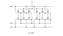
図4に示すように、インバータ307は、3個のPチャネル型TFTを並列に接続した回路と、3個のNチャネル型TFTを並列に接続した回路とによって構成されたインバータ回路を2つ並列に接続した構成をとっている。このように、チャネル幅の小さな(本実施例では30μm)TFTを複数組み合わせて用いることにより、チャネル幅の大きなTFTによってインバータを構成する場合に比較して、TFTのばらつきを解消できる。また、チャネル幅が大きいことによる発熱や劣化などを防ぐことができる。 As shown in FIG. 4, inverter 307, and circuitry connected three P-channel type TFT in parallel, an inverter circuit formed by the three N times to connect the channel type TFT in parallel path 2 In parallel. As described above, by using a plurality of TFTs having a small channel width (30 μm in this embodiment) in combination, the variation in the TFTs can be eliminated as compared to the case where the inverter is configured by the TFTs having a large channel width. Further, it is possible to prevent heat generation and deterioration due to the large channel width.
Applications Claiming Priority (2)
| Application Number | Priority Date | Filing Date | Title |
|---|---|---|---|
| JP10063898 | 1998-03-27 | ||
| JP10-100638 | 1998-03-27 |
Related Parent Applications (1)
| Application Number | Title | Priority Date | Filing Date |
|---|---|---|---|
| JP11047580A Division JPH11338439A (en) | 1998-03-27 | 1999-02-25 | Driving circuit of semiconductor display device and semiconductor display device |
Publications (2)
| Publication Number | Publication Date |
|---|---|
| JP2003308038A JP2003308038A (en) | 2003-10-31 |
| JP2003308038A5 true JP2003308038A5 (en) | 2005-04-07 |
Family
ID=14279380
Family Applications (10)
| Application Number | Title | Priority Date | Filing Date |
|---|---|---|---|
| JP11047580A Withdrawn JPH11338439A (en) | 1998-03-27 | 1999-02-25 | Driving circuit of semiconductor display device and semiconductor display device |
| JP2003008654A Expired - Fee Related JP4198477B2 (en) | 1998-03-27 | 2003-01-16 | Liquid crystal display device driving circuit and liquid crystal display device |
| JP2003008418A Withdrawn JP2003308038A (en) | 1998-03-27 | 2003-01-16 | Driving circuit for semiconductor display device, and semiconductor display device |
| JP2004232866A Expired - Lifetime JP4823494B2 (en) | 1998-03-27 | 2004-08-10 | Semiconductor display device |
| JP2008191294A Withdrawn JP2009025822A (en) | 1998-03-27 | 2008-07-24 | Semiconductor device |
| JP2011178179A Withdrawn JP2012014183A (en) | 1998-03-27 | 2011-08-17 | Buffer circuit |
| JP2013160290A Withdrawn JP2014002396A (en) | 1998-03-27 | 2013-08-01 | Semiconductor device |
| JP2015027715A Withdrawn JP2015146420A (en) | 1998-03-27 | 2015-02-16 | semiconductor device |
| JP2015027716A Expired - Lifetime JP5933776B2 (en) | 1998-03-27 | 2015-02-16 | Semiconductor device |
| JP2016134307A Withdrawn JP2016213863A (en) | 1998-03-27 | 2016-07-06 | Semiconductor device |
Family Applications Before (2)
| Application Number | Title | Priority Date | Filing Date |
|---|---|---|---|
| JP11047580A Withdrawn JPH11338439A (en) | 1998-03-27 | 1999-02-25 | Driving circuit of semiconductor display device and semiconductor display device |
| JP2003008654A Expired - Fee Related JP4198477B2 (en) | 1998-03-27 | 2003-01-16 | Liquid crystal display device driving circuit and liquid crystal display device |
Family Applications After (7)
| Application Number | Title | Priority Date | Filing Date |
|---|---|---|---|
| JP2004232866A Expired - Lifetime JP4823494B2 (en) | 1998-03-27 | 2004-08-10 | Semiconductor display device |
| JP2008191294A Withdrawn JP2009025822A (en) | 1998-03-27 | 2008-07-24 | Semiconductor device |
| JP2011178179A Withdrawn JP2012014183A (en) | 1998-03-27 | 2011-08-17 | Buffer circuit |
| JP2013160290A Withdrawn JP2014002396A (en) | 1998-03-27 | 2013-08-01 | Semiconductor device |
| JP2015027715A Withdrawn JP2015146420A (en) | 1998-03-27 | 2015-02-16 | semiconductor device |
| JP2015027716A Expired - Lifetime JP5933776B2 (en) | 1998-03-27 | 2015-02-16 | Semiconductor device |
| JP2016134307A Withdrawn JP2016213863A (en) | 1998-03-27 | 2016-07-06 | Semiconductor device |
Country Status (4)
| Country | Link |
|---|---|
| US (7) | US6549184B1 (en) |
| JP (10) | JPH11338439A (en) |
| DE (1) | DE19913920A1 (en) |
| TW (1) | TW459267B (en) |
Families Citing this family (44)
| Publication number | Priority date | Publication date | Assignee | Title |
|---|---|---|---|---|
| JP3897826B2 (en) * | 1994-08-19 | 2007-03-28 | 株式会社半導体エネルギー研究所 | Active matrix display device |
| US6686623B2 (en) * | 1997-11-18 | 2004-02-03 | Semiconductor Energy Laboratory Co., Ltd. | Nonvolatile memory and electronic apparatus |
| JP4090569B2 (en) | 1997-12-08 | 2008-05-28 | 株式会社半導体エネルギー研究所 | Semiconductor device, liquid crystal display device, and EL display device |
| JPH11338439A (en) * | 1998-03-27 | 1999-12-10 | Semiconductor Energy Lab Co Ltd | Driving circuit of semiconductor display device and semiconductor display device |
| US6268842B1 (en) * | 1998-04-13 | 2001-07-31 | Semiconductor Energy Laboratory Co., Ltd. | Thin film transistor circuit and semiconductor display device using the same |
| JP2000012864A (en) | 1998-06-22 | 2000-01-14 | Semiconductor Energy Lab Co Ltd | Manufacture of semiconductor device |
| US6271101B1 (en) * | 1998-07-29 | 2001-08-07 | Semiconductor Energy Laboratory Co., Ltd. | Process for production of SOI substrate and process for production of semiconductor device |
| JP3846057B2 (en) * | 1998-09-03 | 2006-11-15 | セイコーエプソン株式会社 | Electro-optical device drive circuit, electro-optical device, and electronic apparatus |
| JP4476390B2 (en) * | 1998-09-04 | 2010-06-09 | 株式会社半導体エネルギー研究所 | Method for manufacturing semiconductor device |
| JP3535067B2 (en) | 2000-03-16 | 2004-06-07 | シャープ株式会社 | Liquid crystal display |
| US6831299B2 (en) | 2000-11-09 | 2004-12-14 | Semiconductor Energy Laboratory Co., Ltd. | Semiconductor device |
| US7700295B2 (en) * | 2000-12-28 | 2010-04-20 | Mds Sciex | Elemental analysis of tagged biologically active materials |
| JP3800401B2 (en) * | 2001-06-18 | 2006-07-26 | 株式会社日立製作所 | Image display apparatus and driving method thereof |
| US7012597B2 (en) * | 2001-08-02 | 2006-03-14 | Seiko Epson Corporation | Supply of a programming current to a pixel |
| US7259740B2 (en) * | 2001-10-03 | 2007-08-21 | Nec Corporation | Display device and semiconductor device |
| KR100940342B1 (en) * | 2001-11-13 | 2010-02-04 | 가부시키가이샤 한도오따이 에네루기 켄큐쇼 | Display device and method for driving the same |
| JP2003332578A (en) | 2002-05-09 | 2003-11-21 | Sharp Corp | Thin film transistor, its manufacturing method, and liquid crystal display device using it |
| JP4683833B2 (en) | 2003-10-31 | 2011-05-18 | 株式会社半導体エネルギー研究所 | Functional circuit and design method thereof |
| SG115733A1 (en) * | 2004-03-12 | 2005-10-28 | Semiconductor Energy Lab | Thin film transistor, semiconductor device, and method for manufacturing the same |
| JP4834853B2 (en) * | 2004-06-10 | 2011-12-14 | シャープ株式会社 | THIN FILM TRANSISTOR CIRCUIT, THIN FILM TRANSISTOR CIRCUIT DESIGN METHOD, THIN FILM TRANSISTOR CIRCUIT DESIGN PROGRAM, DESIGN PROGRAM RECORDING MEDIUM, AND DISPLAY DEVICE |
| EP1863090A1 (en) * | 2006-06-01 | 2007-12-05 | Semiconductor Energy Laboratory Co., Ltd. | Semiconductor device and method for manufacturing semiconductor device |
| JP4720654B2 (en) * | 2006-07-10 | 2011-07-13 | セイコーエプソン株式会社 | Electro-optical device drive circuit, electro-optical device, and electronic apparatus |
| US8654045B2 (en) | 2006-07-31 | 2014-02-18 | Sony Corporation | Display and method for manufacturing display |
| KR101277975B1 (en) * | 2006-09-07 | 2013-06-27 | 엘지디스플레이 주식회사 | Shift resister and data driver having the same, liquid crystal display device |
| US8093601B2 (en) | 2006-09-26 | 2012-01-10 | Sharp Kabushiki Kaisha | Active matrix substrate |
| KR100882696B1 (en) * | 2006-12-21 | 2009-02-06 | 삼성모바일디스플레이주식회사 | Optical Sensor for detecting Peripheral Light and Liquid Crystal Display Device Using the Same |
| JP4456129B2 (en) | 2007-01-31 | 2010-04-28 | シャープ株式会社 | Semiconductor device, liquid crystal display device and electronic apparatus |
| JP2008233536A (en) | 2007-03-20 | 2008-10-02 | Sony Corp | Display device |
| JP2009014796A (en) | 2007-06-30 | 2009-01-22 | Sony Corp | El display panel, power supply line driving device and electronic equipment |
| KR100998488B1 (en) * | 2008-06-25 | 2010-12-06 | 주식회사 하이닉스반도체 | Delay Circuit Structure Including a Plurality of Inverters with different size |
| KR101623958B1 (en) | 2008-10-01 | 2016-05-25 | 삼성전자주식회사 | Inverter, method of operating the same and logic circuit comprising inverter |
| TWI633605B (en) | 2008-10-31 | 2018-08-21 | 半導體能源研究所股份有限公司 | Semiconductor device and method for manufacturing the same |
| TWI525603B (en) | 2009-01-16 | 2016-03-11 | 半導體能源研究所股份有限公司 | Liquid crystal display device and electronic device including the same |
| TW201039307A (en) * | 2009-04-24 | 2010-11-01 | Princeton Technology Corp | Liquid crystal display |
| JP5581261B2 (en) * | 2011-04-27 | 2014-08-27 | 株式会社ジャパンディスプレイ | Semiconductor device, display device and electronic apparatus |
| JP2013068964A (en) * | 2012-11-30 | 2013-04-18 | Panasonic Corp | El display device |
| JP5764185B2 (en) * | 2013-11-22 | 2015-08-12 | 株式会社Joled | EL display device |
| CN103761952B (en) * | 2013-12-31 | 2016-01-27 | 深圳市华星光电技术有限公司 | A kind of scan drive circuit of liquid crystal panel, liquid crystal panel and a kind of driving method |
| CN104537995A (en) * | 2014-12-30 | 2015-04-22 | 深圳市华星光电技术有限公司 | Gate drive circuit and shift register |
| TWI563488B (en) * | 2016-02-01 | 2016-12-21 | Sitronix Technology Corp | Gate driving circuit |
| CN205621414U (en) * | 2016-04-26 | 2016-10-05 | 京东方科技集团股份有限公司 | Electrostatic discharge circuit, array substrate and display device |
| US10541375B2 (en) * | 2016-07-21 | 2020-01-21 | Semiconductor Energy Laboratory Co., Ltd. | Display device and electronic device |
| TWI688812B (en) * | 2018-11-21 | 2020-03-21 | 友達光電股份有限公司 | Display device |
| CN110517628B (en) * | 2019-08-30 | 2021-03-05 | 京东方科技集团股份有限公司 | Display device, grid drive circuit, shift register circuit and drive method thereof |
Family Cites Families (114)
| Publication number | Priority date | Publication date | Assignee | Title |
|---|---|---|---|---|
| US4178605A (en) | 1978-01-30 | 1979-12-11 | Rca Corp. | Complementary MOS inverter structure |
| JPS5710533A (en) * | 1980-06-23 | 1982-01-20 | Nec Corp | Logical circuit |
| GB2081018B (en) | 1980-07-31 | 1985-06-26 | Suwa Seikosha Kk | Active matrix assembly for display device |
| JPS57132191A (en) * | 1981-02-10 | 1982-08-16 | Suwa Seikosha Kk | Active matrix substrate |
| US4330363A (en) | 1980-08-28 | 1982-05-18 | Xerox Corporation | Thermal gradient control for enhanced laser induced crystallization of predefined semiconductor areas |
| JPS58127318A (en) | 1982-01-25 | 1983-07-29 | Nippon Telegr & Teleph Corp <Ntt> | Forming method for single-crystal film on insulating layer |
| JPS58127318U (en) | 1982-02-24 | 1983-08-29 | 株式会社日立製作所 | flow measuring device |
| JPS58176929A (en) | 1982-04-09 | 1983-10-17 | Fujitsu Ltd | Manufacture of semiconductor device |
| US4466179A (en) | 1982-10-19 | 1984-08-21 | Harris Corporation | Method for providing polysilicon thin films of improved uniformity |
| JPS59161014A (en) | 1983-03-03 | 1984-09-11 | Seiko Instr & Electronics Ltd | Crystallization of semiconductor thin film |
| JPS59161014U (en) | 1983-04-14 | 1984-10-29 | 宮田 磯之助 | vertical detector |
| JPH051893Y2 (en) | 1985-09-11 | 1993-01-19 | ||
| AU588693B2 (en) | 1986-05-13 | 1989-09-21 | Sanyo Electric Co., Ltd. | Driving circuit for image display device |
| JPH0628426B2 (en) * | 1986-05-20 | 1994-04-13 | 三洋電機株式会社 | Image display device drive circuit |
| JPH0628425B2 (en) * | 1986-05-20 | 1994-04-13 | 三洋電機株式会社 | Image display device drive circuit |
| JPS62268161A (en) | 1986-05-16 | 1987-11-20 | Hitachi Ltd | Thin-film transistor element |
| JPH065752B2 (en) | 1986-06-25 | 1994-01-19 | 株式会社東芝 | Field effect transistor |
| US4797629A (en) | 1988-03-03 | 1989-01-10 | National Semiconductor Corporation | Wide range operational amplifier input stage |
| US4877980A (en) | 1988-03-10 | 1989-10-31 | Advanced Micro Devices, Inc. | Time variant drive circuit for high speed bus driver to limit oscillations or ringing on a bus |
| JP2653099B2 (en) | 1988-05-17 | 1997-09-10 | セイコーエプソン株式会社 | Active matrix panel, projection display and viewfinder |
| US5274279A (en) | 1988-05-17 | 1993-12-28 | Seiko Epson Corporation | Thin film CMOS inverter |
| JPH0279091A (en) | 1988-09-16 | 1990-03-19 | Hitachi Ltd | Liquid crystal display panel |
| JP2767858B2 (en) | 1989-02-09 | 1998-06-18 | ソニー株式会社 | Liquid crystal display device |
| US4999529A (en) | 1989-06-30 | 1991-03-12 | At&T Bell Laboratories | Programmable logic level input buffer |
| JPH0794744B2 (en) | 1989-08-07 | 1995-10-11 | 昭和コンクリート工業株式会社 | Foamed resin member attached to the earth pressure member |
| JPH03141391A (en) | 1989-10-27 | 1991-06-17 | Fuji Electric Co Ltd | Multioutput driver integrated circuit |
| US5247375A (en) | 1990-03-09 | 1993-09-21 | Hitachi, Ltd. | Display device, manufacturing method thereof and display panel |
| DE69112698T2 (en) * | 1990-05-07 | 1996-02-15 | Fujitsu Ltd | High quality display device with active matrix. |
| JP2973492B2 (en) | 1990-08-22 | 1999-11-08 | ソニー株式会社 | Crystallization method of semiconductor thin film |
| JPH04313732A (en) * | 1990-12-29 | 1992-11-05 | Semiconductor Energy Lab Co Ltd | Television receiver |
| JPH04282869A (en) | 1991-03-11 | 1992-10-07 | G T C:Kk | Manufacturing method of thin film semiconductor device and device for executing this |
| JP2587546B2 (en) | 1991-03-22 | 1997-03-05 | 株式会社ジーティシー | Scanning circuit |
| US5365875A (en) | 1991-03-25 | 1994-11-22 | Fuji Xerox Co., Ltd. | Semiconductor element manufacturing method |
| JP2927051B2 (en) | 1991-06-25 | 1999-07-28 | 株式会社デンソー | Heat exchanger |
| GB9114018D0 (en) | 1991-06-28 | 1991-08-14 | Philips Electronic Associated | Thin-film transistor manufacture |
| JPH0591447A (en) | 1991-09-25 | 1993-04-09 | Toshiba Corp | Transmissive liquid crystal display device |
| KR100269350B1 (en) | 1991-11-26 | 2000-10-16 | 구본준 | Manufacturing Method of Thin Film Transistor |
| JPH0726573Y2 (en) | 1991-12-16 | 1995-06-14 | 正一 山口 | Seal nut |
| JPH05175235A (en) | 1991-12-25 | 1993-07-13 | Sharp Corp | Manufacture of polycrystalline semiconductor thin film |
| US5227679A (en) | 1992-01-02 | 1993-07-13 | Advanced Micro Devices, Inc. | Cmos digital-controlled delay gate |
| US5256916A (en) | 1992-02-18 | 1993-10-26 | National Semiconductor Corporation | TTL to CMOS translating input buffer circuit with dual thresholds for high dynamic current and low static current |
| US5372836A (en) | 1992-03-27 | 1994-12-13 | Tokyo Electron Limited | Method of forming polycrystalling silicon film in process of manufacturing LCD |
| GB9207527D0 (en) | 1992-04-07 | 1992-05-20 | Philips Electronics Uk Ltd | Multi-standard video matrix display apparatus and its method of operation |
| US5250852A (en) * | 1992-04-16 | 1993-10-05 | Texas Instruments Incorporated | Circuitry and method for latching a logic state |
| JP3240681B2 (en) | 1992-04-24 | 2001-12-17 | セイコーエプソン株式会社 | Active matrix panel drive circuit and active matrix panel |
| US5627557A (en) | 1992-08-20 | 1997-05-06 | Sharp Kabushiki Kaisha | Display apparatus |
| JP2697507B2 (en) | 1992-08-28 | 1998-01-14 | セイコーエプソン株式会社 | Liquid crystal display |
| JPH06123896A (en) | 1992-10-13 | 1994-05-06 | Toshiba Corp | Liquid crystal display device |
| US5413958A (en) | 1992-11-16 | 1995-05-09 | Tokyo Electron Limited | Method for manufacturing a liquid crystal display substrate |
| US5403762A (en) | 1993-06-30 | 1995-04-04 | Semiconductor Energy Laboratory Co., Ltd. | Method of fabricating a TFT |
| US5459337A (en) * | 1993-02-19 | 1995-10-17 | Sony Corporation | Semiconductor display device with red, green and blue emission |
| US5471225A (en) * | 1993-04-28 | 1995-11-28 | Dell Usa, L.P. | Liquid crystal display with integrated frame buffer |
| US5594569A (en) | 1993-07-22 | 1997-01-14 | Semiconductor Energy Laboratory Co., Ltd. | Liquid-crystal electro-optical apparatus and method of manufacturing the same |
| US5610414A (en) | 1993-07-28 | 1997-03-11 | Sharp Kabushiki Kaisha | Semiconductor device |
| US5589406A (en) | 1993-07-30 | 1996-12-31 | Ag Technology Co., Ltd. | Method of making TFT display |
| US5477073A (en) | 1993-08-20 | 1995-12-19 | Casio Computer Co., Ltd. | Thin film semiconductor device including a driver and a matrix circuit |
| US5566080A (en) | 1993-09-07 | 1996-10-15 | Fujitsu Limited | Method and apparatus for designing semiconductor device |
| WO1995007493A1 (en) * | 1993-09-09 | 1995-03-16 | Kabushiki Kaisha Toshiba | Display device and its driving method |
| JPH0794744A (en) | 1993-09-20 | 1995-04-07 | Hitachi Ltd | Mis transistor |
| TW264575B (en) | 1993-10-29 | 1995-12-01 | Handotai Energy Kenkyusho Kk | |
| JP3431033B2 (en) | 1993-10-29 | 2003-07-28 | 株式会社半導体エネルギー研究所 | Semiconductor fabrication method |
| US5923962A (en) | 1993-10-29 | 1999-07-13 | Semiconductor Energy Laboratory Co., Ltd. | Method for manufacturing a semiconductor device |
| TW299897U (en) | 1993-11-05 | 1997-03-01 | Semiconductor Energy Lab | A semiconductor integrated circuit |
| JP2759415B2 (en) | 1993-11-05 | 1998-05-28 | 株式会社半導体エネルギー研究所 | Method for manufacturing semiconductor device |
| JPH07147411A (en) * | 1993-11-24 | 1995-06-06 | Sony Corp | Semiconductor device for display element substrate use |
| JP3277056B2 (en) | 1993-12-09 | 2002-04-22 | シャープ株式会社 | Signal amplification circuit and image display device using the same |
| US5734366A (en) | 1993-12-09 | 1998-03-31 | Sharp Kabushiki Kaisha | Signal amplifier, signal amplifier circuit, signal line drive circuit and image display device |
| TW255032B (en) * | 1993-12-20 | 1995-08-21 | Sharp Kk | |
| JPH07181927A (en) | 1993-12-24 | 1995-07-21 | Sharp Corp | Image display device |
| TW277129B (en) | 1993-12-24 | 1996-06-01 | Sharp Kk | |
| JP3442449B2 (en) | 1993-12-25 | 2003-09-02 | 株式会社半導体エネルギー研究所 | Display device and its driving circuit |
| US5616935A (en) * | 1994-02-08 | 1997-04-01 | Semiconductor Energy Laboratory Co., Ltd. | Semiconductor integrated circuit having N-channel and P-channel transistors |
| TW280037B (en) | 1994-04-22 | 1996-07-01 | Handotai Energy Kenkyusho Kk | Drive circuit of active matrix type display device and manufacturing method |
| JPH07294961A (en) | 1994-04-22 | 1995-11-10 | Semiconductor Energy Lab Co Ltd | Drive circuit and design method for active matrix type display device |
| JP3101178B2 (en) | 1994-04-22 | 2000-10-23 | 株式会社半導体エネルギー研究所 | Drive circuit for active matrix display device and method of manufacturing the same |
| JP3407975B2 (en) | 1994-05-20 | 2003-05-19 | 株式会社半導体エネルギー研究所 | Thin film semiconductor integrated circuit |
| JPH07327185A (en) | 1994-05-31 | 1995-12-12 | Sharp Corp | Sampling circuit and image display device using it |
| CN1136529C (en) | 1994-05-31 | 2004-01-28 | 夏普株式会社 | Sampling circuit, signal amplifier, and image display |
| JP3897826B2 (en) | 1994-08-19 | 2007-03-28 | 株式会社半導体エネルギー研究所 | Active matrix display device |
| JP3464287B2 (en) | 1994-09-05 | 2003-11-05 | 株式会社半導体エネルギー研究所 | Method for manufacturing semiconductor device |
| JP3382026B2 (en) * | 1994-09-13 | 2003-03-04 | 株式会社東芝 | Clock signal distribution circuit, buffer circuit and design method thereof |
| JP2815311B2 (en) | 1994-09-28 | 1998-10-27 | インターナショナル・ビジネス・マシーンズ・コーポレイション | Driving device and method for liquid crystal display device |
| JPH08125027A (en) | 1994-10-24 | 1996-05-17 | Yozan:Kk | Formation method for mos inverter circuit |
| DE69525707T2 (en) | 1994-09-30 | 2002-08-01 | Yozan Inc | MOS inverter circuit |
| DE19540146B4 (en) | 1994-10-27 | 2012-06-21 | Nec Corp. | Active matrix liquid crystal display with drivers for multimedia applications and driving methods therefor |
| JPH08146918A (en) | 1994-11-18 | 1996-06-07 | Sony Corp | Switching device and switching method |
| CN1099608C (en) | 1994-11-21 | 2003-01-22 | 精工爱普生株式会社 | Liquid crystal driving device, liquid crystal display device, analog buffer, and liquid crystal driving method |
| JP3469337B2 (en) | 1994-12-16 | 2003-11-25 | 株式会社半導体エネルギー研究所 | Method for manufacturing semiconductor device |
| JPH08264802A (en) | 1995-03-28 | 1996-10-11 | Semiconductor Energy Lab Co Ltd | Manufacture of semiconductor, manufacture of thin film transistor and thin film transistor |
| US5956581A (en) | 1995-04-20 | 1999-09-21 | Semiconductor Energy Laboratory Co., Ltd. | Method of manufacturing a semiconductor device |
| JP3234131B2 (en) | 1995-06-23 | 2001-12-04 | 株式会社東芝 | Liquid crystal display |
| JPH098314A (en) * | 1995-06-26 | 1997-01-10 | Sharp Corp | Thin film transistor |
| JP3286152B2 (en) * | 1995-06-29 | 2002-05-27 | シャープ株式会社 | Thin film transistor circuit and image display device |
| JPH0936730A (en) | 1995-07-19 | 1997-02-07 | Yozan:Kk | Inverter circuit |
| JP3514002B2 (en) | 1995-09-04 | 2004-03-31 | カシオ計算機株式会社 | Display drive |
| JP3256110B2 (en) | 1995-09-28 | 2002-02-12 | シャープ株式会社 | Liquid crystal display |
| KR100205259B1 (en) | 1996-03-04 | 1999-07-01 | 구자홍 | A driving circuit for liquid crystal display of active matrix type |
| JP3338281B2 (en) | 1996-03-19 | 2002-10-28 | 株式会社東芝 | LCD panel |
| JPH09260962A (en) * | 1996-03-19 | 1997-10-03 | Sharp Corp | Inverter circuit and amplifier |
| JPH09330059A (en) * | 1996-06-13 | 1997-12-22 | Hitachi Ltd | Liquid crystal display device |
| US6084248A (en) | 1996-06-28 | 2000-07-04 | Seiko Epson Corporation | Thin film transistor, manufacturing method thereof, and circuit and liquid crystal display device using the thin film transistor |
| US7195960B2 (en) | 1996-06-28 | 2007-03-27 | Seiko Epson Corporation | Thin film transistor, manufacturing method thereof, and circuit and liquid crystal display device using the thin film transistor |
| US6429120B1 (en) | 2000-01-18 | 2002-08-06 | Micron Technology, Inc. | Methods and apparatus for making integrated-circuit wiring from copper, silver, gold, and other metals |
| JP4307574B2 (en) | 1996-09-03 | 2009-08-05 | 株式会社半導体エネルギー研究所 | Active matrix display device |
| US5945970A (en) | 1996-09-06 | 1999-08-31 | Samsung Electronics Co., Ltd. | Liquid crystal display devices having improved screen clearing capability and methods of operating same |
| JP3795606B2 (en) | 1996-12-30 | 2006-07-12 | 株式会社半導体エネルギー研究所 | Circuit and liquid crystal display device using the same |
| JP3915194B2 (en) | 1997-10-09 | 2007-05-16 | 石川島播磨重工業株式会社 | Die cushion raising method and apparatus |
| JPH11214700A (en) | 1998-01-23 | 1999-08-06 | Semiconductor Energy Lab Co Ltd | Semiconductor display device |
| JPH11338439A (en) | 1998-03-27 | 1999-12-10 | Semiconductor Energy Lab Co Ltd | Driving circuit of semiconductor display device and semiconductor display device |
| US6268842B1 (en) | 1998-04-13 | 2001-07-31 | Semiconductor Energy Laboratory Co., Ltd. | Thin film transistor circuit and semiconductor display device using the same |
| JP3844613B2 (en) | 1998-04-28 | 2006-11-15 | 株式会社半導体エネルギー研究所 | Thin film transistor circuit and display device using the same |
| US6831299B2 (en) | 2000-11-09 | 2004-12-14 | Semiconductor Energy Laboratory Co., Ltd. | Semiconductor device |
| WO2005041301A1 (en) | 2003-10-23 | 2005-05-06 | Nec Corporation | Semiconductor device and production method therefor |
| JP5042518B2 (en) | 2006-04-12 | 2012-10-03 | ルネサスエレクトロニクス株式会社 | Semiconductor device |
-
1999
- 1999-02-25 JP JP11047580A patent/JPH11338439A/en not_active Withdrawn
- 1999-03-24 US US09/275,426 patent/US6549184B1/en not_active Expired - Lifetime
- 1999-03-24 TW TW088104655A patent/TW459267B/en not_active IP Right Cessation
- 1999-03-26 DE DE19913920A patent/DE19913920A1/en not_active Withdrawn
-
2003
- 2003-01-14 US US10/341,470 patent/US7304625B2/en not_active Expired - Fee Related
- 2003-01-16 JP JP2003008654A patent/JP4198477B2/en not_active Expired - Fee Related
- 2003-01-16 JP JP2003008418A patent/JP2003308038A/en not_active Withdrawn
-
2004
- 2004-04-20 US US10/827,438 patent/US7315296B2/en not_active Expired - Fee Related
- 2004-08-10 JP JP2004232866A patent/JP4823494B2/en not_active Expired - Lifetime
-
2007
- 2007-12-31 US US12/003,698 patent/US8054270B2/en not_active Expired - Fee Related
-
2008
- 2008-07-24 JP JP2008191294A patent/JP2009025822A/en not_active Withdrawn
-
2011
- 2011-08-17 JP JP2011178179A patent/JP2012014183A/en not_active Withdrawn
- 2011-11-04 US US13/289,488 patent/US8373631B2/en not_active Expired - Fee Related
-
2013
- 2013-02-11 US US13/763,895 patent/US8629823B2/en not_active Expired - Fee Related
- 2013-08-01 JP JP2013160290A patent/JP2014002396A/en not_active Withdrawn
-
2014
- 2014-01-13 US US14/153,667 patent/US9262978B2/en not_active Expired - Fee Related
-
2015
- 2015-02-16 JP JP2015027715A patent/JP2015146420A/en not_active Withdrawn
- 2015-02-16 JP JP2015027716A patent/JP5933776B2/en not_active Expired - Lifetime
-
2016
- 2016-07-06 JP JP2016134307A patent/JP2016213863A/en not_active Withdrawn
Similar Documents
| Publication | Publication Date | Title |
|---|---|---|
| JP2003308038A5 (en) | ||
| TW200731586A (en) | Thermoelectric conversion module, heat exchanger equipped with the same, and thermoelectric power-generating device | |
| JP2012209362A5 (en) | ||
| JP2005045016A5 (en) | ||
| PA8542201A1 (en) | PCP INHIBITORS BASED ON ACIDS-3-HETEROCICLYLPROPANOHYDROXAMICS | |
| JP2003168803A5 (en) | ||
| JP2008507923A5 (en) | ||
| TH93509S (en) | Semiconductor device | |
| TH29136S1 (en) | Semiconductor device | |
| TH96412S (en) | bathtub | |
| TH84529S (en) | Pattern on the package | |
| TH74420S (en) | Power generator | |
| TH28163S1 (en) | Packaging | |
| TH110757S (en) | Devices for connection | |
| TH28477S1 (en) | bathtub | |
| TH80893S (en) | Evaporative dosing device | |
| TH80892S (en) | Evaporative dosing device | |
| TH28485S1 (en) | Evaporative dosing device | |
| TH26555S1 (en) | bathtub | |
| TH24975S1 (en) | Pattern on the box | |
| TH22652S1 (en) | Fan parts | |
| TH79712S (en) | Fan parts | |
| TH75635S (en) | glove | |
| TH31164S1 (en) | Refrigerator | |
| TH62234S (en) | plate |