EP4583646A2 - Anzeigevorrichtung - Google Patents
Anzeigevorrichtung Download PDFInfo
- Publication number
- EP4583646A2 EP4583646A2 EP25178878.2A EP25178878A EP4583646A2 EP 4583646 A2 EP4583646 A2 EP 4583646A2 EP 25178878 A EP25178878 A EP 25178878A EP 4583646 A2 EP4583646 A2 EP 4583646A2
- Authority
- EP
- European Patent Office
- Prior art keywords
- display
- face
- display panel
- rear plate
- light
- Prior art date
- Legal status (The legal status is an assumption and is not a legal conclusion. Google has not performed a legal analysis and makes no representation as to the accuracy of the status listed.)
- Pending
Links
Images


Classifications
-
- G—PHYSICS
- G02—OPTICS
- G02F—OPTICAL DEVICES OR ARRANGEMENTS FOR THE CONTROL OF LIGHT BY MODIFICATION OF THE OPTICAL PROPERTIES OF THE MEDIA OF THE ELEMENTS INVOLVED THEREIN; NON-LINEAR OPTICS; FREQUENCY-CHANGING OF LIGHT; OPTICAL LOGIC ELEMENTS; OPTICAL ANALOGUE/DIGITAL CONVERTERS
- G02F1/00—Devices or arrangements for the control of the intensity, colour, phase, polarisation or direction of light arriving from an independent light source, e.g. switching, gating or modulating; Non-linear optics
- G02F1/01—Devices or arrangements for the control of the intensity, colour, phase, polarisation or direction of light arriving from an independent light source, e.g. switching, gating or modulating; Non-linear optics for the control of the intensity, phase, polarisation or colour
- G02F1/13—Devices or arrangements for the control of the intensity, colour, phase, polarisation or direction of light arriving from an independent light source, e.g. switching, gating or modulating; Non-linear optics for the control of the intensity, phase, polarisation or colour based on liquid crystals, e.g. single liquid crystal display cells
- G02F1/133—Constructional arrangements; Operation of liquid crystal cells; Circuit arrangements
- G02F1/1333—Constructional arrangements; Manufacturing methods
- G02F1/133308—Support structures for LCD panels, e.g. frames or bezels
-
- F—MECHANICAL ENGINEERING; LIGHTING; HEATING; WEAPONS; BLASTING
- F21—LIGHTING
- F21V—FUNCTIONAL FEATURES OR DETAILS OF LIGHTING DEVICES OR SYSTEMS THEREOF; STRUCTURAL COMBINATIONS OF LIGHTING DEVICES WITH OTHER ARTICLES, NOT OTHERWISE PROVIDED FOR
- F21V11/00—Screens not covered by groups F21V1/00, F21V3/00, F21V7/00 or F21V9/00
-
- G—PHYSICS
- G02—OPTICS
- G02B—OPTICAL ELEMENTS, SYSTEMS OR APPARATUS
- G02B6/00—Light guides; Structural details of arrangements comprising light guides and other optical elements, e.g. couplings
- G02B6/0001—Light guides; Structural details of arrangements comprising light guides and other optical elements, e.g. couplings specially adapted for lighting devices or systems
- G02B6/0011—Light guides; Structural details of arrangements comprising light guides and other optical elements, e.g. couplings specially adapted for lighting devices or systems the light guides being planar or of plate-like form
-
- G—PHYSICS
- G02—OPTICS
- G02F—OPTICAL DEVICES OR ARRANGEMENTS FOR THE CONTROL OF LIGHT BY MODIFICATION OF THE OPTICAL PROPERTIES OF THE MEDIA OF THE ELEMENTS INVOLVED THEREIN; NON-LINEAR OPTICS; FREQUENCY-CHANGING OF LIGHT; OPTICAL LOGIC ELEMENTS; OPTICAL ANALOGUE/DIGITAL CONVERTERS
- G02F1/00—Devices or arrangements for the control of the intensity, colour, phase, polarisation or direction of light arriving from an independent light source, e.g. switching, gating or modulating; Non-linear optics
- G02F1/01—Devices or arrangements for the control of the intensity, colour, phase, polarisation or direction of light arriving from an independent light source, e.g. switching, gating or modulating; Non-linear optics for the control of the intensity, phase, polarisation or colour
- G02F1/13—Devices or arrangements for the control of the intensity, colour, phase, polarisation or direction of light arriving from an independent light source, e.g. switching, gating or modulating; Non-linear optics for the control of the intensity, phase, polarisation or colour based on liquid crystals, e.g. single liquid crystal display cells
- G02F1/133—Constructional arrangements; Operation of liquid crystal cells; Circuit arrangements
- G02F1/1333—Constructional arrangements; Manufacturing methods
- G02F1/1335—Structural association of cells with optical devices, e.g. polarisers or reflectors
- G02F1/1336—Illuminating devices
- G02F1/133602—Direct backlight
- G02F1/133608—Direct backlight including particular frames or supporting means
-
- G—PHYSICS
- G09—EDUCATION; CRYPTOGRAPHY; DISPLAY; ADVERTISING; SEALS
- G09F—DISPLAYING; ADVERTISING; SIGNS; LABELS OR NAME-PLATES; SEALS
- G09F9/00—Indicating arrangements for variable information in which the information is built-up on a support by selection or combination of individual elements
- G09F9/30—Indicating arrangements for variable information in which the information is built-up on a support by selection or combination of individual elements in which the desired character or characters are formed by combining individual elements
-
- H—ELECTRICITY
- H05—ELECTRIC TECHNIQUES NOT OTHERWISE PROVIDED FOR
- H05B—ELECTRIC HEATING; ELECTRIC LIGHT SOURCES NOT OTHERWISE PROVIDED FOR; CIRCUIT ARRANGEMENTS FOR ELECTRIC LIGHT SOURCES, IN GENERAL
- H05B33/00—Electroluminescent light sources
- H05B33/12—Light sources with substantially two-dimensional [2D] radiating surfaces
- H05B33/22—Light sources with substantially two-dimensional [2D] radiating surfaces characterised by the chemical or physical composition or the arrangement of auxiliary dielectric or reflective layers
-
- H—ELECTRICITY
- H05—ELECTRIC TECHNIQUES NOT OTHERWISE PROVIDED FOR
- H05K—PRINTED CIRCUITS; CASINGS OR CONSTRUCTIONAL DETAILS OF ELECTRIC APPARATUS; MANUFACTURE OF ASSEMBLAGES OF ELECTRICAL COMPONENTS
- H05K7/00—Constructional details common to different types of electric apparatus
- H05K7/02—Arrangements of circuit components or wiring on supporting structure
- H05K7/023—Stackable modules
-
- H—ELECTRICITY
- H05—ELECTRIC TECHNIQUES NOT OTHERWISE PROVIDED FOR
- H05K—PRINTED CIRCUITS; CASINGS OR CONSTRUCTIONAL DETAILS OF ELECTRIC APPARATUS; MANUFACTURE OF ASSEMBLAGES OF ELECTRICAL COMPONENTS
- H05K7/00—Constructional details common to different types of electric apparatus
- H05K7/14—Mounting supporting structure in casing or on frame or rack
- H05K7/1422—Printed circuit boards receptacles, e.g. stacked structures, electronic circuit modules or box like frames
- H05K7/1427—Housings
-
- G—PHYSICS
- G02—OPTICS
- G02B—OPTICAL ELEMENTS, SYSTEMS OR APPARATUS
- G02B6/00—Light guides; Structural details of arrangements comprising light guides and other optical elements, e.g. couplings
- G02B6/0001—Light guides; Structural details of arrangements comprising light guides and other optical elements, e.g. couplings specially adapted for lighting devices or systems
- G02B6/0011—Light guides; Structural details of arrangements comprising light guides and other optical elements, e.g. couplings specially adapted for lighting devices or systems the light guides being planar or of plate-like form
- G02B6/0033—Means for improving the coupling-out of light from the light guide
- G02B6/0035—Means for improving the coupling-out of light from the light guide provided on the surface of the light guide or in the bulk of it
- G02B6/004—Scattering dots or dot-like elements, e.g. microbeads, scattering particles, nanoparticles
- G02B6/0041—Scattering dots or dot-like elements, e.g. microbeads, scattering particles, nanoparticles provided in the bulk of the light guide
-
- G—PHYSICS
- G02—OPTICS
- G02B—OPTICAL ELEMENTS, SYSTEMS OR APPARATUS
- G02B6/00—Light guides; Structural details of arrangements comprising light guides and other optical elements, e.g. couplings
- G02B6/0001—Light guides; Structural details of arrangements comprising light guides and other optical elements, e.g. couplings specially adapted for lighting devices or systems
- G02B6/0011—Light guides; Structural details of arrangements comprising light guides and other optical elements, e.g. couplings specially adapted for lighting devices or systems the light guides being planar or of plate-like form
- G02B6/0081—Mechanical or electrical aspects of the light guide and light source in the lighting device peculiar to the adaptation to planar light guides, e.g. concerning packaging
- G02B6/0086—Positioning aspects
- G02B6/0088—Positioning aspects of the light guide or other optical sheets in the package
-
- G—PHYSICS
- G02—OPTICS
- G02B—OPTICAL ELEMENTS, SYSTEMS OR APPARATUS
- G02B6/00—Light guides; Structural details of arrangements comprising light guides and other optical elements, e.g. couplings
- G02B6/0001—Light guides; Structural details of arrangements comprising light guides and other optical elements, e.g. couplings specially adapted for lighting devices or systems
- G02B6/0011—Light guides; Structural details of arrangements comprising light guides and other optical elements, e.g. couplings specially adapted for lighting devices or systems the light guides being planar or of plate-like form
- G02B6/0081—Mechanical or electrical aspects of the light guide and light source in the lighting device peculiar to the adaptation to planar light guides, e.g. concerning packaging
- G02B6/0093—Means for protecting the light guide
-
- G—PHYSICS
- G02—OPTICS
- G02F—OPTICAL DEVICES OR ARRANGEMENTS FOR THE CONTROL OF LIGHT BY MODIFICATION OF THE OPTICAL PROPERTIES OF THE MEDIA OF THE ELEMENTS INVOLVED THEREIN; NON-LINEAR OPTICS; FREQUENCY-CHANGING OF LIGHT; OPTICAL LOGIC ELEMENTS; OPTICAL ANALOGUE/DIGITAL CONVERTERS
- G02F1/00—Devices or arrangements for the control of the intensity, colour, phase, polarisation or direction of light arriving from an independent light source, e.g. switching, gating or modulating; Non-linear optics
- G02F1/01—Devices or arrangements for the control of the intensity, colour, phase, polarisation or direction of light arriving from an independent light source, e.g. switching, gating or modulating; Non-linear optics for the control of the intensity, phase, polarisation or colour
- G02F1/13—Devices or arrangements for the control of the intensity, colour, phase, polarisation or direction of light arriving from an independent light source, e.g. switching, gating or modulating; Non-linear optics for the control of the intensity, phase, polarisation or colour based on liquid crystals, e.g. single liquid crystal display cells
- G02F1/133—Constructional arrangements; Operation of liquid crystal cells; Circuit arrangements
- G02F1/1333—Constructional arrangements; Manufacturing methods
- G02F1/133302—Rigid substrates, e.g. inorganic substrates
-
- G—PHYSICS
- G02—OPTICS
- G02F—OPTICAL DEVICES OR ARRANGEMENTS FOR THE CONTROL OF LIGHT BY MODIFICATION OF THE OPTICAL PROPERTIES OF THE MEDIA OF THE ELEMENTS INVOLVED THEREIN; NON-LINEAR OPTICS; FREQUENCY-CHANGING OF LIGHT; OPTICAL LOGIC ELEMENTS; OPTICAL ANALOGUE/DIGITAL CONVERTERS
- G02F1/00—Devices or arrangements for the control of the intensity, colour, phase, polarisation or direction of light arriving from an independent light source, e.g. switching, gating or modulating; Non-linear optics
- G02F1/01—Devices or arrangements for the control of the intensity, colour, phase, polarisation or direction of light arriving from an independent light source, e.g. switching, gating or modulating; Non-linear optics for the control of the intensity, phase, polarisation or colour
- G02F1/13—Devices or arrangements for the control of the intensity, colour, phase, polarisation or direction of light arriving from an independent light source, e.g. switching, gating or modulating; Non-linear optics for the control of the intensity, phase, polarisation or colour based on liquid crystals, e.g. single liquid crystal display cells
- G02F1/133—Constructional arrangements; Operation of liquid crystal cells; Circuit arrangements
- G02F1/1333—Constructional arrangements; Manufacturing methods
- G02F1/133308—Support structures for LCD panels, e.g. frames or bezels
- G02F1/133314—Back frames
-
- G—PHYSICS
- G02—OPTICS
- G02F—OPTICAL DEVICES OR ARRANGEMENTS FOR THE CONTROL OF LIGHT BY MODIFICATION OF THE OPTICAL PROPERTIES OF THE MEDIA OF THE ELEMENTS INVOLVED THEREIN; NON-LINEAR OPTICS; FREQUENCY-CHANGING OF LIGHT; OPTICAL LOGIC ELEMENTS; OPTICAL ANALOGUE/DIGITAL CONVERTERS
- G02F1/00—Devices or arrangements for the control of the intensity, colour, phase, polarisation or direction of light arriving from an independent light source, e.g. switching, gating or modulating; Non-linear optics
- G02F1/01—Devices or arrangements for the control of the intensity, colour, phase, polarisation or direction of light arriving from an independent light source, e.g. switching, gating or modulating; Non-linear optics for the control of the intensity, phase, polarisation or colour
- G02F1/13—Devices or arrangements for the control of the intensity, colour, phase, polarisation or direction of light arriving from an independent light source, e.g. switching, gating or modulating; Non-linear optics for the control of the intensity, phase, polarisation or colour based on liquid crystals, e.g. single liquid crystal display cells
- G02F1/133—Constructional arrangements; Operation of liquid crystal cells; Circuit arrangements
- G02F1/1333—Constructional arrangements; Manufacturing methods
- G02F1/133308—Support structures for LCD panels, e.g. frames or bezels
- G02F1/133317—Intermediate frames, e.g. between backlight housing and front frame
-
- G—PHYSICS
- G02—OPTICS
- G02F—OPTICAL DEVICES OR ARRANGEMENTS FOR THE CONTROL OF LIGHT BY MODIFICATION OF THE OPTICAL PROPERTIES OF THE MEDIA OF THE ELEMENTS INVOLVED THEREIN; NON-LINEAR OPTICS; FREQUENCY-CHANGING OF LIGHT; OPTICAL LOGIC ELEMENTS; OPTICAL ANALOGUE/DIGITAL CONVERTERS
- G02F1/00—Devices or arrangements for the control of the intensity, colour, phase, polarisation or direction of light arriving from an independent light source, e.g. switching, gating or modulating; Non-linear optics
- G02F1/01—Devices or arrangements for the control of the intensity, colour, phase, polarisation or direction of light arriving from an independent light source, e.g. switching, gating or modulating; Non-linear optics for the control of the intensity, phase, polarisation or colour
- G02F1/13—Devices or arrangements for the control of the intensity, colour, phase, polarisation or direction of light arriving from an independent light source, e.g. switching, gating or modulating; Non-linear optics for the control of the intensity, phase, polarisation or colour based on liquid crystals, e.g. single liquid crystal display cells
- G02F1/133—Constructional arrangements; Operation of liquid crystal cells; Circuit arrangements
- G02F1/1333—Constructional arrangements; Manufacturing methods
- G02F1/133308—Support structures for LCD panels, e.g. frames or bezels
- G02F1/13332—Front frames
-
- G—PHYSICS
- G02—OPTICS
- G02F—OPTICAL DEVICES OR ARRANGEMENTS FOR THE CONTROL OF LIGHT BY MODIFICATION OF THE OPTICAL PROPERTIES OF THE MEDIA OF THE ELEMENTS INVOLVED THEREIN; NON-LINEAR OPTICS; FREQUENCY-CHANGING OF LIGHT; OPTICAL LOGIC ELEMENTS; OPTICAL ANALOGUE/DIGITAL CONVERTERS
- G02F1/00—Devices or arrangements for the control of the intensity, colour, phase, polarisation or direction of light arriving from an independent light source, e.g. switching, gating or modulating; Non-linear optics
- G02F1/01—Devices or arrangements for the control of the intensity, colour, phase, polarisation or direction of light arriving from an independent light source, e.g. switching, gating or modulating; Non-linear optics for the control of the intensity, phase, polarisation or colour
- G02F1/13—Devices or arrangements for the control of the intensity, colour, phase, polarisation or direction of light arriving from an independent light source, e.g. switching, gating or modulating; Non-linear optics for the control of the intensity, phase, polarisation or colour based on liquid crystals, e.g. single liquid crystal display cells
- G02F1/133—Constructional arrangements; Operation of liquid crystal cells; Circuit arrangements
- G02F1/1333—Constructional arrangements; Manufacturing methods
- G02F1/133308—Support structures for LCD panels, e.g. frames or bezels
- G02F1/133331—Cover glasses
-
- G—PHYSICS
- G02—OPTICS
- G02F—OPTICAL DEVICES OR ARRANGEMENTS FOR THE CONTROL OF LIGHT BY MODIFICATION OF THE OPTICAL PROPERTIES OF THE MEDIA OF THE ELEMENTS INVOLVED THEREIN; NON-LINEAR OPTICS; FREQUENCY-CHANGING OF LIGHT; OPTICAL LOGIC ELEMENTS; OPTICAL ANALOGUE/DIGITAL CONVERTERS
- G02F1/00—Devices or arrangements for the control of the intensity, colour, phase, polarisation or direction of light arriving from an independent light source, e.g. switching, gating or modulating; Non-linear optics
- G02F1/01—Devices or arrangements for the control of the intensity, colour, phase, polarisation or direction of light arriving from an independent light source, e.g. switching, gating or modulating; Non-linear optics for the control of the intensity, phase, polarisation or colour
- G02F1/13—Devices or arrangements for the control of the intensity, colour, phase, polarisation or direction of light arriving from an independent light source, e.g. switching, gating or modulating; Non-linear optics for the control of the intensity, phase, polarisation or colour based on liquid crystals, e.g. single liquid crystal display cells
- G02F1/133—Constructional arrangements; Operation of liquid crystal cells; Circuit arrangements
- G02F1/1333—Constructional arrangements; Manufacturing methods
- G02F1/1335—Structural association of cells with optical devices, e.g. polarisers or reflectors
- G02F1/133509—Filters, e.g. light shielding masks
- G02F1/133514—Colour filters
-
- G—PHYSICS
- G02—OPTICS
- G02F—OPTICAL DEVICES OR ARRANGEMENTS FOR THE CONTROL OF LIGHT BY MODIFICATION OF THE OPTICAL PROPERTIES OF THE MEDIA OF THE ELEMENTS INVOLVED THEREIN; NON-LINEAR OPTICS; FREQUENCY-CHANGING OF LIGHT; OPTICAL LOGIC ELEMENTS; OPTICAL ANALOGUE/DIGITAL CONVERTERS
- G02F1/00—Devices or arrangements for the control of the intensity, colour, phase, polarisation or direction of light arriving from an independent light source, e.g. switching, gating or modulating; Non-linear optics
- G02F1/01—Devices or arrangements for the control of the intensity, colour, phase, polarisation or direction of light arriving from an independent light source, e.g. switching, gating or modulating; Non-linear optics for the control of the intensity, phase, polarisation or colour
- G02F1/13—Devices or arrangements for the control of the intensity, colour, phase, polarisation or direction of light arriving from an independent light source, e.g. switching, gating or modulating; Non-linear optics for the control of the intensity, phase, polarisation or colour based on liquid crystals, e.g. single liquid crystal display cells
- G02F1/133—Constructional arrangements; Operation of liquid crystal cells; Circuit arrangements
- G02F1/1333—Constructional arrangements; Manufacturing methods
- G02F1/1335—Structural association of cells with optical devices, e.g. polarisers or reflectors
- G02F1/133528—Polarisers
-
- G—PHYSICS
- G02—OPTICS
- G02F—OPTICAL DEVICES OR ARRANGEMENTS FOR THE CONTROL OF LIGHT BY MODIFICATION OF THE OPTICAL PROPERTIES OF THE MEDIA OF THE ELEMENTS INVOLVED THEREIN; NON-LINEAR OPTICS; FREQUENCY-CHANGING OF LIGHT; OPTICAL LOGIC ELEMENTS; OPTICAL ANALOGUE/DIGITAL CONVERTERS
- G02F1/00—Devices or arrangements for the control of the intensity, colour, phase, polarisation or direction of light arriving from an independent light source, e.g. switching, gating or modulating; Non-linear optics
- G02F1/01—Devices or arrangements for the control of the intensity, colour, phase, polarisation or direction of light arriving from an independent light source, e.g. switching, gating or modulating; Non-linear optics for the control of the intensity, phase, polarisation or colour
- G02F1/13—Devices or arrangements for the control of the intensity, colour, phase, polarisation or direction of light arriving from an independent light source, e.g. switching, gating or modulating; Non-linear optics for the control of the intensity, phase, polarisation or colour based on liquid crystals, e.g. single liquid crystal display cells
- G02F1/133—Constructional arrangements; Operation of liquid crystal cells; Circuit arrangements
- G02F1/1333—Constructional arrangements; Manufacturing methods
- G02F1/1343—Electrodes
- G02F1/13439—Electrodes characterised by their electrical, optical, physical properties; materials therefor; method of making
-
- G—PHYSICS
- G02—OPTICS
- G02F—OPTICAL DEVICES OR ARRANGEMENTS FOR THE CONTROL OF LIGHT BY MODIFICATION OF THE OPTICAL PROPERTIES OF THE MEDIA OF THE ELEMENTS INVOLVED THEREIN; NON-LINEAR OPTICS; FREQUENCY-CHANGING OF LIGHT; OPTICAL LOGIC ELEMENTS; OPTICAL ANALOGUE/DIGITAL CONVERTERS
- G02F1/00—Devices or arrangements for the control of the intensity, colour, phase, polarisation or direction of light arriving from an independent light source, e.g. switching, gating or modulating; Non-linear optics
- G02F1/01—Devices or arrangements for the control of the intensity, colour, phase, polarisation or direction of light arriving from an independent light source, e.g. switching, gating or modulating; Non-linear optics for the control of the intensity, phase, polarisation or colour
- G02F1/13—Devices or arrangements for the control of the intensity, colour, phase, polarisation or direction of light arriving from an independent light source, e.g. switching, gating or modulating; Non-linear optics for the control of the intensity, phase, polarisation or colour based on liquid crystals, e.g. single liquid crystal display cells
- G02F1/133—Constructional arrangements; Operation of liquid crystal cells; Circuit arrangements
- G02F1/136—Liquid crystal cells structurally associated with a semi-conducting layer or substrate, e.g. cells forming part of an integrated circuit
- G02F1/1362—Active matrix addressed cells
- G02F1/1368—Active matrix addressed cells in which the switching element is a three-electrode device
-
- G—PHYSICS
- G02—OPTICS
- G02F—OPTICAL DEVICES OR ARRANGEMENTS FOR THE CONTROL OF LIGHT BY MODIFICATION OF THE OPTICAL PROPERTIES OF THE MEDIA OF THE ELEMENTS INVOLVED THEREIN; NON-LINEAR OPTICS; FREQUENCY-CHANGING OF LIGHT; OPTICAL LOGIC ELEMENTS; OPTICAL ANALOGUE/DIGITAL CONVERTERS
- G02F1/00—Devices or arrangements for the control of the intensity, colour, phase, polarisation or direction of light arriving from an independent light source, e.g. switching, gating or modulating; Non-linear optics
- G02F1/01—Devices or arrangements for the control of the intensity, colour, phase, polarisation or direction of light arriving from an independent light source, e.g. switching, gating or modulating; Non-linear optics for the control of the intensity, phase, polarisation or colour
- G02F1/13—Devices or arrangements for the control of the intensity, colour, phase, polarisation or direction of light arriving from an independent light source, e.g. switching, gating or modulating; Non-linear optics for the control of the intensity, phase, polarisation or colour based on liquid crystals, e.g. single liquid crystal display cells
- G02F1/137—Devices or arrangements for the control of the intensity, colour, phase, polarisation or direction of light arriving from an independent light source, e.g. switching, gating or modulating; Non-linear optics for the control of the intensity, phase, polarisation or colour based on liquid crystals, e.g. single liquid crystal display cells characterised by the electro-optical or magneto-optical effect, e.g. field-induced phase transition, orientation effect, guest-host interaction or dynamic scattering
-
- G—PHYSICS
- G02—OPTICS
- G02F—OPTICAL DEVICES OR ARRANGEMENTS FOR THE CONTROL OF LIGHT BY MODIFICATION OF THE OPTICAL PROPERTIES OF THE MEDIA OF THE ELEMENTS INVOLVED THEREIN; NON-LINEAR OPTICS; FREQUENCY-CHANGING OF LIGHT; OPTICAL LOGIC ELEMENTS; OPTICAL ANALOGUE/DIGITAL CONVERTERS
- G02F1/00—Devices or arrangements for the control of the intensity, colour, phase, polarisation or direction of light arriving from an independent light source, e.g. switching, gating or modulating; Non-linear optics
- G02F1/01—Devices or arrangements for the control of the intensity, colour, phase, polarisation or direction of light arriving from an independent light source, e.g. switching, gating or modulating; Non-linear optics for the control of the intensity, phase, polarisation or colour
- G02F1/13—Devices or arrangements for the control of the intensity, colour, phase, polarisation or direction of light arriving from an independent light source, e.g. switching, gating or modulating; Non-linear optics for the control of the intensity, phase, polarisation or colour based on liquid crystals, e.g. single liquid crystal display cells
- G02F1/137—Devices or arrangements for the control of the intensity, colour, phase, polarisation or direction of light arriving from an independent light source, e.g. switching, gating or modulating; Non-linear optics for the control of the intensity, phase, polarisation or colour based on liquid crystals, e.g. single liquid crystal display cells characterised by the electro-optical or magneto-optical effect, e.g. field-induced phase transition, orientation effect, guest-host interaction or dynamic scattering
- G02F1/13712—Devices or arrangements for the control of the intensity, colour, phase, polarisation or direction of light arriving from an independent light source, e.g. switching, gating or modulating; Non-linear optics for the control of the intensity, phase, polarisation or colour based on liquid crystals, e.g. single liquid crystal display cells characterised by the electro-optical or magneto-optical effect, e.g. field-induced phase transition, orientation effect, guest-host interaction or dynamic scattering the liquid crystal having negative dielectric anisotropy
-
- G—PHYSICS
- G02—OPTICS
- G02F—OPTICAL DEVICES OR ARRANGEMENTS FOR THE CONTROL OF LIGHT BY MODIFICATION OF THE OPTICAL PROPERTIES OF THE MEDIA OF THE ELEMENTS INVOLVED THEREIN; NON-LINEAR OPTICS; FREQUENCY-CHANGING OF LIGHT; OPTICAL LOGIC ELEMENTS; OPTICAL ANALOGUE/DIGITAL CONVERTERS
- G02F2201/00—Constructional arrangements not provided for in groups G02F1/00 - G02F7/00
- G02F2201/12—Constructional arrangements not provided for in groups G02F1/00 - G02F7/00 electrode
- G02F2201/123—Constructional arrangements not provided for in groups G02F1/00 - G02F7/00 electrode pixel
Definitions
- a display panel is contained in a housing, and this housing is configured of a front-face housing and a rear-face housing.
- the front-face housing includes a front bezel, a top chassis, and the like provided on a display surface side of the display panel.
- the rear-face housing includes a back chassis, a frame, back-face cover, and the like covering a back-face side of the display panel (for example, see Patent Literature 1).
- Patent Literature 1 Japanese Unexamined Patent Application Publication No. 2008-304630
- the housing containing the liquid crystal panel, the rear-face housing in particular is configured of a plurality of members such as the back chassis, the frame, the back-face cover, and the like, which has prevented a reduction in thickness.
- a display according to an embodiment of the present technology includes: a display panel; and a back-face member having rigidity and provided on a back face of the display panel, the back-face member covering the back face, or the back face and other part of the display panel.
- the back-face member covering the back face of the display panel is configured of a rigid member, and thus, it is possible to simplify a member configuration.
- a member having rigidity is used as the back-face member of the display panel. Therefore, the configuration of the back-face member is simplified, and thereby, it is possible to reduce the thickness of the display.
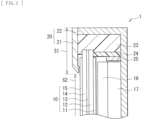
- FIG. 1 is a diagram illustrating a cross-sectional configuration of a display (a display 1) according to a first embodiment of the present disclosure
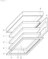
- FIG. 2 is an exploded perspective view illustrating an overall configuration of the display 1.
- the display 1 may be, for example, a liquid crystal display used as a television device.
- This display 1 has a configuration in which: a backlight unit is contained in a housing 20 including a front bezel 21 (front-face member) and a back chassis 22 (back-face member); the backlight unit includes a display panel 10, an optical sheet 16, a light-guiding plate 17, a light source 18, and the like; and the front bezel 21 and the back chassis 22 are adhered to each other with an adhesion member 23.
- a plurality of LEDs are arranged as the light source 18, and light emitted from this light source 18 irradiates the display panel 10 via the light-guiding plate 17, and is extracted as display light toward the front bezel 21.
- the display panel 10 displays an image such as a moving image or a still image, and may be, for example, a liquid crystal display panel having a liquid crystal layer 13 between two substrates, i.e., a TFT substrate 12 and a CF substrate 14. Further, polarizing plates 11 and 15 allowing polarized light in a specific direction to pass therethrough are provided on a surface (front face (display surface) of the TFT substrate 12 and a surface (back face) of the CF substrate 14, respectively, the surfaces being opposite to surfaces where the liquid crystal layer 13 is provided.
- the TFT substrate 12 may be configured by, for example, arranging a plurality of pixel electrodes (not illustrated) in a matrix on a glass substrate.
- This TFT substrate 12 is provided with TFT (Thin Film Transistor) devices driving the respective pixel electrodes, gate lines and source lines connected to these TFT devices, and the like (none is illustrated).
- the pixel electrodes may be formed of, for example, a conductive material having transparency such as ITO (Indium Tin Oxide), and are each provided for every sub-pixel (not illustrated) on the glass substrate.
- the CF substrate 14 may have, for example, a color filter (not illustrated) with, for example, stripe-shaped filters of red (R), green (G), and blue (B) on a glass substrate, and may have a counter electrode (not illustrated) over almost the entire surface of an effective display region S2 on this color filter.
- the counter electrode may be configured using, for example, a conductive material having transparency such as ITO, like the pixel electrodes described above. It is to be noted that, although not illustrated here, a spacer may be provided between the counter electrode and the pixel electrodes on the TFT substrate 12 side, thereby keeping a gap between these substrates.
- the liquid crystal layer 13 may include liquid crystal molecules having negative dielectric constant anisotropy, and a polymer structure holding the liquid crystal molecules in proximity to an interface with an alignment film (not illustrated).
- a liquid crystal molecule has a property in which a dielectric constant in a major axis direction is larger than that in a minor axis direction. Based on this property, the liquid crystal molecule is arranged to allow the major axis of the liquid crystal molecule to be perpendicular to a substrate when a drive voltage is OFF, and the liquid crystal molecule is oriented to allow the major axis of the liquid crystal molecule to be parallel to the substrate when the drive voltage is ON. Thus, an image is displayed on the liquid crystal display panel.
- the light source 18 for example, in addition to a white LED (Light Emitting Diode), LEDs emitting light of red, blue, green, and the like may be used. Further, other than a point light source such as LED, a linear light source such as a fluorescent light may be used. As illustrated in FIG. 2 , here, the light source 18 is provided on the one end surface (undersurface) of the light-guiding plate 17, but is not limited to this, and may be disposed along four sides of the light-guiding plate 17.
- a white LED Light Emitting Diode
- LEDs emitting light of red, blue, green, and the like may be used.
- a linear light source such as a fluorescent light may be used.
- the light source 18 is provided on the one end surface (undersurface) of the light-guiding plate 17, but is not limited to this, and may be disposed along four sides of the light-guiding plate 17.
- the housing 20 may be, for example, substantially shaped like a rectangular solid, and has two opposed surfaces, namely, a display surface and a back face, and also has side faces between these two surfaces.
- the housing 20 in the present embodiment is configured of a front-face plate (the front bezel 21) and a back-face plate (the back chassis 22).
- the front-face plate covers at least part of a front face of the display panel 10 (for example, a circumferential edge portion of the display panel 10), and the back-face plate covers a back face and side faces between the front face and the back face of the display panel 10.
- the back chassis 22 is also used to fix the display panel 10, while covering at least the back face of the display panel 10, and, here, covering the back face and the side faces between and the front face and the back face of the display panel 10 as described above.
- metal having high thermal conductivity specifically, Al may be used, as with the front bezel 21.
- Fe or the like can be used.
- the front bezel 21 and the back chassis 22 are adhered to each other with the adhesion member 23 (sealant).
- a connection member for example, a middle chassis or the like used to connect the front bezel 21 and the back chassis 22 to each other is omitted by integrating the front bezel 21 and the back chassis 22 with this adhesion member 23.
- the adhesion member 23 may include adhesives having sufficient adhesive strength and elasticity, which are, specifically, adhesives such as acrylic resin, urethane resin, epoxy resin, vinyl chloride resin, and modified silicone resin.
- FIG. 3 illustrates a cross-sectional configuration of a display 2 according to the second embodiment of the present disclosure.
- the display 2 includes the display panel 10, the optical sheet 16, and the light-guiding plate 17 contained in a housing 30, and the display 2 is different from the display of the first embodiment in that this housing 30 is configured of a front bezel 31 (front-face member), a rear plate 32 (back-face member), a top chassis 33, and a middle chassis 34.
- the housing 30 may be, for example, substantially shaped like a rectangular solid, and has two opposed surfaces, namely, a display surface and a back face, and also has side surfaces between these two surfaces.
- the front bezel 31 and the rear plate 32 are connected with the top chassis 33 and the middle chassis 34.
- the front bezel 31 serves as a front-face plate covering the display surface (front face) and the side faces of the display panel 10.
- the rear plate 32 serves as a back-face plate covering a back face of the display panel 10.
- the top chassis 33 and the middle chassis 34 are provided to connect the front bezel 31 and the rear plate 32 to each other as described above.
- Examples of a material of each of the top chassis 33 and the middle chassis 34 may include metal such as Al and Fe, similarly to the material of the back chassis 22 in the above-described first embodiment.
- the top chassis 33 and the middle chassis 34 may be molded using a material having thermal conductivity lower than that of metal, which is, for example, a synthetic resin or the like. Use of the material having low thermal conductivity suppresses transmission of heat produced in the light source 18 to the front bezel 31, and makes it possible to radiate heat from the back-face side efficiently, while suppressing a temperature rise on the front-face side of the display 2.
- this display 2 light emitted from the light source 18 enters the display panel 10 through the light-guiding plate 17 and the optical sheet 16, in a manner similar to that in the above-described first embodiment.
- This entered light passes through the polarizing plate 11, and then passes through the liquid crystal layer 13, while being modulated for every pixel, based on an image voltage applied between transparent electrodes of the TFT substrate 12 and the CF substrate 14. After passing through the liquid crystal layer 13, the light passes through a color filter, thereby being extracted as color display light to an outer side (a surface side) of the polarizing plate 15.
- FIG. 7 illustrates the cross-sectional configuration of the display 100 of the related art.
- a back-face housing including the back chassis 122 and the like, and the outer member including the rear cover 125 and the like are provided to contain the display panel 110 and support the entire display 100.
- the back-face plate (the rear plate 32) having rigidity is used for the entire back face of the display panel 10, of the housing 30 containing the display panel 10. This allows one member to serve in place of a plurality of members including the back chassis 122, the rear cover 125, and the like used to support the typical display 100.
- FIG. 4 illustrates a cross-sectional configuration of a display 3 according to a third embodiment of the present disclosure.
- the display 3 includes the display panel 10, the optical sheet 16, and the light-guiding plate 17 contained in a housing 40, and the display 3 is different from the first and second embodiments in that this housing 40 is configured of a front glass 41 (front-face member, transparent plate), a rear plate 42 (back-face member), and a decoration frame 43, the front glass 41 being provided on a front face of the display panel 10 with a sealing layer 44 in between.
- the front glass 41 (front-face member), the rear plate 42 (back-face member), and the decoration frame 43 are adhered to one another with the adhesion member 23.
- the front glass 41 is a plate-like member provided on the entire front face of the display panel 10 with the sealing layer 44 in between as described above, and is configured using a material of high transparency, such as glass, polycarbonate (PC), and plastic in which ABS resin is added to PC.
- the front glass 41 has, for example, a thickness of about 0.5 mm to about 3.5 mm both inclusive, and protects an display region S2 of the display panel 10, and also supports the display 3 in cooperation with the rear plate 42 which will be described later.
- the rear plate 42 is provided to cover the entire back-face side of the display panel 10 as described above, and also to support the entire display 3, as in the above-described second embodiment.
- the rear plate 42 is a member having rigidity, and may be made of, for example, glass or metal such as Al and Fe having a thickness of about 1.0 mm to about 3.0 mm both inclusive.
- the front glass 41 and the rear plate 42 are adhered to each other with the adhesion member 23 as described above. Therefore, materials having the same or similar properties may be preferably used as the materials of the front glass 41 and the rear plate 42.
- glass may be desirably used in view of transparency desired for the front glass 41, rigidity desired for a support member of the display, and a difference in expansion coefficient with respect to the display panel 10. Further, on the entire back face of the rear plate 42, a light-shielding film 42A is provided to prevent entrance of external light into the display 3, as in the above-described second embodiment.
- the decoration frame 43 is provided to cover side faces between a front face and a back face of the display 3, and also to seal the adhesion member 23 used to connect the front glass 41 and the rear plate 42 to each other.
- a material of the decoration frame 43 for example, the material of the back chassis 22 in the above-described first embodiment, metal such as Al and Fe, or the like may be used.
- the decoration frame 43 may be a flat-plate-like member, but as illustrated in FIG. 4 , the decoration frame 43 may have a protrusion section 43A in a sealing direction of the adhesion member 23. By providing this protrusion section 43A, an amount of the adhesion member 23 used to adhere the front glass 41 and the rear plate 42 to each other may be reduced.
- positioning of members configuring the display 3 (for example, see FIG. 5 ) may be performed by appropriately adjusting a position where the protrusion section 43A is formed.
- FIG. 5 illustrates a cross-sectional configuration of a display 4 according to a fourth embodiment of the present disclosure.
- the display panel 10 and the optical sheet 16 are contained in a housing 50, and this housing 50 is configured of a front glass 51 (front-face member) provided on a front face of the display panel 10 with the sealing layer 44 in between, a light-guiding plate 52 (back-face member), and a decoration frame 53.
- the light-guiding plate 52 is used as a back-face member, which is different from the above-described first to third embodiments. It is to be noted that the front glass 51, the light-guiding plate 52, and the decoration frame 53 are adhered to one another with the adhesion member 23.
- the middle chassis 64 are provided to connect the display panel 10 and the rear plate 62 to each other as described above.
- a material of the middle chassis 64 for example, the material of the back chassis 22 in the above-described first embodiment, metal such as Al and Fe, and/or the like may be used. It is to be noted that a material having lower thermal conductivity than metal, for example, a material such as a synthetic resin may be used for molding.
- the middle chassis 64 may be configured, for example, of four members that are dividable into top, bottom, right, and left members when the display panel 10 is rectangular.
- the front-face member is not provided, and the display panel 10 and the rear plate 62 that is formed of a material having rigidity and serves as the back-face member are connected to each other with the middle chassis 64. Therefore, it is possible to further reduce the thickness in addition to the effects in the above-described second embodiment. Further, it is possible to reduce the number of components configuring the display 5. Therefore, cost is allowed to be further slimmed down, and the weight of the display 5 is allowed to be reduced.
- the present technology has been described using the first to fifth embodiments, but the present technology is not limited to the above-described embodiments and may be variously modified.
- the liquid crystal display is used as an example of the display 1 in the above-described embodiment, but a plasma display, an organic electroluminescence display, or the like may be adopted.
- each of the members and thicknesses in the above-described embodiments is described as an example. Not all the members may necessarily be provided, or other members may be further provided.
- a heat sink may be adhered to part or all of the back face of the display, for example, to a lower end part where the light source 18 is provided.
- metal superior in thermal conductivity may be desirably used, and, for example, a material formed by molding a block made of Al or the like may be used.
- the polarizing plate is provided on a surface of the display panel, but is not limited to this example, and may be, for example, provided on a surface of the front glass.
Landscapes
- Physics & Mathematics (AREA)
- General Physics & Mathematics (AREA)
- Nonlinear Science (AREA)
- Engineering & Computer Science (AREA)
- Optics & Photonics (AREA)
- Mathematical Physics (AREA)
- Chemical & Material Sciences (AREA)
- Crystallography & Structural Chemistry (AREA)
- Microelectronics & Electronic Packaging (AREA)
- Theoretical Computer Science (AREA)
- General Engineering & Computer Science (AREA)
- Liquid Crystal (AREA)
- Devices For Indicating Variable Information By Combining Individual Elements (AREA)
Applications Claiming Priority (7)
| Application Number | Priority Date | Filing Date | Title |
|---|---|---|---|
| JP2011116243 | 2011-05-24 | ||
| JP2012102345A JP2013008016A (ja) | 2011-05-24 | 2012-04-27 | 表示装置 |
| EP21153800.4A EP3859439A1 (de) | 2011-05-24 | 2012-05-24 | Anzeige |
| PCT/JP2012/063344 WO2012161260A1 (ja) | 2011-05-24 | 2012-05-24 | 表示装置 |
| EP18180325.5A EP3444658B1 (de) | 2011-05-24 | 2012-05-24 | Anzeige |
| EP16184986.4A EP3112929B1 (de) | 2011-05-24 | 2012-05-24 | Anzeige |
| EP12790195.7A EP2717090B1 (de) | 2011-05-24 | 2012-05-24 | Anzeigevorrichtung |
Related Parent Applications (4)
| Application Number | Title | Priority Date | Filing Date |
|---|---|---|---|
| EP16184986.4A Division EP3112929B1 (de) | 2011-05-24 | 2012-05-24 | Anzeige |
| EP18180325.5A Division EP3444658B1 (de) | 2011-05-24 | 2012-05-24 | Anzeige |
| EP21153800.4A Division EP3859439A1 (de) | 2011-05-24 | 2012-05-24 | Anzeige |
| EP12790195.7A Division EP2717090B1 (de) | 2011-05-24 | 2012-05-24 | Anzeigevorrichtung |
Publications (2)
| Publication Number | Publication Date |
|---|---|
| EP4583646A2 true EP4583646A2 (de) | 2025-07-09 |
| EP4583646A3 EP4583646A3 (de) | 2025-09-17 |
Family
ID=47217332
Family Applications (5)
| Application Number | Title | Priority Date | Filing Date |
|---|---|---|---|
| EP12790195.7A Active EP2717090B1 (de) | 2011-05-24 | 2012-05-24 | Anzeigevorrichtung |
| EP18180325.5A Active EP3444658B1 (de) | 2011-05-24 | 2012-05-24 | Anzeige |
| EP16184986.4A Active EP3112929B1 (de) | 2011-05-24 | 2012-05-24 | Anzeige |
| EP21153800.4A Withdrawn EP3859439A1 (de) | 2011-05-24 | 2012-05-24 | Anzeige |
| EP25178878.2A Pending EP4583646A3 (de) | 2011-05-24 | 2012-05-24 | Anzeigevorrichtung |
Family Applications Before (4)
| Application Number | Title | Priority Date | Filing Date |
|---|---|---|---|
| EP12790195.7A Active EP2717090B1 (de) | 2011-05-24 | 2012-05-24 | Anzeigevorrichtung |
| EP18180325.5A Active EP3444658B1 (de) | 2011-05-24 | 2012-05-24 | Anzeige |
| EP16184986.4A Active EP3112929B1 (de) | 2011-05-24 | 2012-05-24 | Anzeige |
| EP21153800.4A Withdrawn EP3859439A1 (de) | 2011-05-24 | 2012-05-24 | Anzeige |
Country Status (5)
| Country | Link |
|---|---|
| US (6) | US9277667B2 (de) |
| EP (5) | EP2717090B1 (de) |
| JP (1) | JP2013008016A (de) |
| DE (1) | DE202012013458U1 (de) |
| WO (1) | WO2012161260A1 (de) |
Families Citing this family (32)
| Publication number | Priority date | Publication date | Assignee | Title |
|---|---|---|---|---|
| JP2013008016A (ja) | 2011-05-24 | 2013-01-10 | Sony Corp | 表示装置 |
| JP6312072B2 (ja) * | 2012-12-26 | 2018-04-18 | 株式会社ジャパンディスプレイ | 液晶表示装置 |
| KR20220025259A (ko) * | 2013-07-19 | 2022-03-03 | 가부시키가이샤 한도오따이 에네루기 켄큐쇼 | 반도체 장치 |
| JP2015232651A (ja) * | 2014-06-10 | 2015-12-24 | キヤノン株式会社 | 画像表示装置 |
| US9781853B1 (en) * | 2014-06-12 | 2017-10-03 | Amazon Technologies, Inc. | Display stack enclosure |
| US10042110B2 (en) * | 2014-07-21 | 2018-08-07 | Samsung Display Co., Ltd. | Liquid crystal display and manufacturing method thereof |
| TWI521277B (zh) * | 2014-08-28 | 2016-02-11 | 揚昇照明股份有限公司 | 顯示裝置 |
| EP3187927B1 (de) * | 2014-08-28 | 2022-06-29 | Sony Group Corporation | Anzeigevorrichtung und beleuchtungsvorrichtung |
| JP6601398B2 (ja) * | 2014-08-28 | 2019-11-06 | ソニー株式会社 | 表示装置 |
| US20170199417A1 (en) * | 2014-09-19 | 2017-07-13 | Panasonic Intellectual Property Management Co., Ltd. | Display device |
| KR20160068439A (ko) * | 2014-12-05 | 2016-06-15 | 삼성전자주식회사 | 하이브리드 터치 기반 전자 장치 및 그 제어 방법 |
| JP6405227B2 (ja) * | 2014-12-19 | 2018-10-17 | 古野電気株式会社 | 表示装置及び表示装置製造方法 |
| US9995956B2 (en) * | 2015-03-20 | 2018-06-12 | Opton (Shunchang) Optics Co., Ltd | Integrated fully-sealed liquid cryatal screen and manufacturing process for same |
| KR102428657B1 (ko) * | 2015-10-27 | 2022-08-03 | 엘지전자 주식회사 | 디스플레이 디바이스 |
| KR102396460B1 (ko) * | 2015-10-29 | 2022-05-11 | 엘지디스플레이 주식회사 | 곡면부를 갖는 표시 장치 및 이를 포함하는 전자 장치 |
| KR20170119361A (ko) * | 2016-04-18 | 2017-10-27 | 삼성디스플레이 주식회사 | 표시 장치 |
| WO2017203816A1 (ja) * | 2016-05-25 | 2017-11-30 | ソニー株式会社 | 発光ユニット、液晶モジュール、表示装置および照明装置 |
| JP6848219B2 (ja) * | 2016-06-10 | 2021-03-24 | 株式会社リコー | 画像表示装置 |
| JP2018004728A (ja) * | 2016-06-28 | 2018-01-11 | 株式会社ジャパンディスプレイ | 表示装置および接着方法 |
| US10534227B2 (en) * | 2016-09-19 | 2020-01-14 | Lg Display Co., Ltd. | Integrated display module and ultra-slim display device |
| KR102545158B1 (ko) * | 2016-10-31 | 2023-06-20 | 엘지디스플레이 주식회사 | 디스플레이 장치 |
| KR102543807B1 (ko) * | 2016-10-31 | 2023-06-16 | 엘지디스플레이 주식회사 | 디스플레이 장치 |
| KR102721410B1 (ko) * | 2016-11-23 | 2024-10-23 | 엘지디스플레이 주식회사 | 액정표시장치 |
| KR102552047B1 (ko) | 2016-11-24 | 2023-07-07 | 엘지디스플레이 주식회사 | 디스플레이 장치 |
| EP3678367B1 (de) | 2017-08-28 | 2023-12-13 | LG Electronics Inc. | Anzeigevorrichtung |
| CN107479254A (zh) * | 2017-09-22 | 2017-12-15 | 青岛海信电器股份有限公司 | 一种背板、背光模组和液晶显示装置 |
| CN110827687B (zh) * | 2018-12-05 | 2022-05-10 | 友达光电股份有限公司 | 显示装置 |
| JP6991448B2 (ja) * | 2018-12-20 | 2022-02-03 | トライベイル テクノロジーズ, エルエルシー | 表示装置 |
| KR102682500B1 (ko) * | 2019-03-26 | 2024-07-08 | 삼성디스플레이 주식회사 | 폴더블 표시 장치와 그의 음향 제공 방법 |
| JP2020201438A (ja) * | 2019-06-12 | 2020-12-17 | シャープ株式会社 | 表示装置 |
| JP7324991B2 (ja) * | 2021-07-19 | 2023-08-14 | 日亜化学工業株式会社 | 面状光源及び表示装置 |
| KR20250092707A (ko) * | 2023-12-15 | 2025-06-24 | 엘지디스플레이 주식회사 | 디스플레이장치 및 그 제조방법 |
Citations (3)
| Publication number | Priority date | Publication date | Assignee | Title |
|---|---|---|---|---|
| JP2008304630A (ja) | 2007-06-06 | 2008-12-18 | Hitachi Ltd | 液晶表示装置 |
| JP2011116243A (ja) | 2009-12-03 | 2011-06-16 | Mazda Motor Corp | 車両のバッテリ配設構造 |
| JP2012102345A (ja) | 2010-11-05 | 2012-05-31 | Osaka Prefecture Univ | コアシェル粒子の製造方法 |
Family Cites Families (28)
| Publication number | Priority date | Publication date | Assignee | Title |
|---|---|---|---|---|
| US5701055A (en) * | 1994-03-13 | 1997-12-23 | Pioneer Electronic Corporation | Organic electoluminescent display panel and method for manufacturing the same |
| JPH11352479A (ja) | 1998-06-12 | 1999-12-24 | Dainippon Printing Co Ltd | バックライト装置及び透過型表示装置 |
| KR100666321B1 (ko) * | 2000-06-30 | 2007-01-09 | 삼성전자주식회사 | 적층형 백라이트 어셈블리, 이를 적용한 액정표시장치 및이들의 조립 방법 |
| CN1582461A (zh) * | 2001-09-07 | 2005-02-16 | 松下电器产业株式会社 | 显示装置及其制造方法 |
| US20030063231A1 (en) * | 2001-09-28 | 2003-04-03 | Yuan-Tung Dai | LCD panel integrated with oled |
| JP4261888B2 (ja) | 2001-12-25 | 2009-04-30 | キヤノン株式会社 | 表示装置 |
| JP3891843B2 (ja) * | 2002-01-08 | 2007-03-14 | 株式会社日立製作所 | 液晶表示装置 |
| JP4163567B2 (ja) * | 2003-07-09 | 2008-10-08 | 株式会社 日立ディスプレイズ | 発光型表示装置 |
| US6967439B2 (en) * | 2004-02-24 | 2005-11-22 | Eastman Kodak Company | OLED display having thermally conductive backplate |
| KR101189088B1 (ko) | 2005-06-22 | 2012-11-09 | 삼성디스플레이 주식회사 | 백라이트 어셈블리 및 이를 갖는 액정표시장치 |
| WO2008032557A1 (en) * | 2006-09-12 | 2008-03-20 | Konica Minolta Holdings, Inc. | Organic electroluminescence element, and illuminating device and display device provided with the organic electroluminescence element |
| JP2008103150A (ja) * | 2006-10-18 | 2008-05-01 | Mitsubishi Electric Corp | 面状光源装置 |
| US7786559B2 (en) * | 2006-11-08 | 2010-08-31 | Corning Incorporated | Bezel packaging of frit-sealed OLED devices |
| DE202006017277U1 (de) * | 2006-11-13 | 2007-01-18 | Element Displays Dr. Wiemer Gmbh | Flüssigkristall-Anzeigevorrichtung |
| JP2008304680A (ja) | 2007-06-07 | 2008-12-18 | Fuji Xerox Co Ltd | 画像形成装置と露光量補正方法とプログラム |
| JP5026163B2 (ja) * | 2007-06-26 | 2012-09-12 | セイコーインスツル株式会社 | 電子機器 |
| FR2920551B1 (fr) * | 2007-08-31 | 2010-04-23 | Thales Sa | Dispositif a ecran plat comportant un boitier de protection transparent |
| JP4575486B2 (ja) * | 2007-10-24 | 2010-11-04 | セイコーインスツル株式会社 | 表示装置 |
| US20090154198A1 (en) | 2007-12-14 | 2009-06-18 | Joo Hoon Lee | Reflection type display apparatus |
| EP2251771B1 (de) | 2008-01-30 | 2017-05-31 | Kyocera Corporation | Berührungsschirm und berührungsschirmdisplay |
| JP2010157957A (ja) | 2009-01-05 | 2010-07-15 | Panasonic Corp | 表示装置及び表示装置を備える携帯端末装置 |
| JP5399417B2 (ja) | 2009-01-13 | 2014-01-29 | シャープ株式会社 | 表示装置及びバックライト装置 |
| US8456586B2 (en) * | 2009-06-11 | 2013-06-04 | Apple Inc. | Portable computer display structures |
| KR101710647B1 (ko) * | 2009-08-25 | 2017-02-27 | 삼성전자 주식회사 | 디스플레이장치 및 이를 갖는 휴대용 컴퓨터 |
| KR101394936B1 (ko) * | 2009-11-06 | 2014-05-14 | 엘지디스플레이 주식회사 | 광차단층을 갖는 평판 표시 장치 |
| US8551283B2 (en) | 2010-02-02 | 2013-10-08 | Apple Inc. | Offset control for assembling an electronic device housing |
| US8576202B2 (en) * | 2010-03-25 | 2013-11-05 | Elo Touch Solutions, Inc. | Bezel-less acoustic touch apparatus |
| JP2013008016A (ja) * | 2011-05-24 | 2013-01-10 | Sony Corp | 表示装置 |
-
2012
- 2012-04-27 JP JP2012102345A patent/JP2013008016A/ja active Pending
- 2012-05-24 DE DE202012013458.2U patent/DE202012013458U1/de not_active Expired - Lifetime
- 2012-05-24 EP EP12790195.7A patent/EP2717090B1/de active Active
- 2012-05-24 EP EP18180325.5A patent/EP3444658B1/de active Active
- 2012-05-24 EP EP16184986.4A patent/EP3112929B1/de active Active
- 2012-05-24 EP EP21153800.4A patent/EP3859439A1/de not_active Withdrawn
- 2012-05-24 WO PCT/JP2012/063344 patent/WO2012161260A1/ja not_active Ceased
- 2012-05-24 EP EP25178878.2A patent/EP4583646A3/de active Pending
- 2012-05-24 US US14/118,051 patent/US9277667B2/en active Active
-
2015
- 2015-09-11 US US14/851,099 patent/US9332660B2/en active Active
-
2016
- 2016-03-07 US US15/062,420 patent/US10268059B2/en active Active
- 2016-10-05 US US15/285,957 patent/US10288918B2/en active Active
-
2019
- 2019-03-11 US US16/298,572 patent/US10613364B2/en active Active
-
2020
- 2020-02-26 US US16/801,859 patent/US10976582B2/en active Active
Patent Citations (3)
| Publication number | Priority date | Publication date | Assignee | Title |
|---|---|---|---|---|
| JP2008304630A (ja) | 2007-06-06 | 2008-12-18 | Hitachi Ltd | 液晶表示装置 |
| JP2011116243A (ja) | 2009-12-03 | 2011-06-16 | Mazda Motor Corp | 車両のバッテリ配設構造 |
| JP2012102345A (ja) | 2010-11-05 | 2012-05-31 | Osaka Prefecture Univ | コアシェル粒子の製造方法 |
Also Published As
| Publication number | Publication date |
|---|---|
| US20140092631A1 (en) | 2014-04-03 |
| US10268059B2 (en) | 2019-04-23 |
| US20170023821A1 (en) | 2017-01-26 |
| JP2013008016A (ja) | 2013-01-10 |
| EP3112929B1 (de) | 2018-12-05 |
| US9277667B2 (en) | 2016-03-01 |
| DE202012013458U1 (de) | 2017-02-02 |
| EP3444658A1 (de) | 2019-02-20 |
| US9332660B2 (en) | 2016-05-03 |
| EP3859439A1 (de) | 2021-08-04 |
| US20150382487A1 (en) | 2015-12-31 |
| US20160192512A1 (en) | 2016-06-30 |
| US10976582B2 (en) | 2021-04-13 |
| US20200192143A1 (en) | 2020-06-18 |
| WO2012161260A1 (ja) | 2012-11-29 |
| EP3444658B1 (de) | 2021-03-03 |
| US10613364B2 (en) | 2020-04-07 |
| US20190204662A1 (en) | 2019-07-04 |
| US10288918B2 (en) | 2019-05-14 |
| EP3112929A1 (de) | 2017-01-04 |
| EP4583646A3 (de) | 2025-09-17 |
| EP2717090A1 (de) | 2014-04-09 |
| EP2717090A4 (de) | 2015-06-03 |
| EP2717090B1 (de) | 2018-04-11 |
Similar Documents
| Publication | Publication Date | Title |
|---|---|---|
| US10976582B2 (en) | Display | |
| US9274361B2 (en) | Display | |
| US10795200B2 (en) | Display device | |
| US10042195B2 (en) | Display | |
| US9939686B2 (en) | Display device |
Legal Events
| Date | Code | Title | Description |
|---|---|---|---|
| PUAI | Public reference made under article 153(3) epc to a published international application that has entered the european phase |
Free format text: ORIGINAL CODE: 0009012 |
|
| STAA | Information on the status of an ep patent application or granted ep patent |
Free format text: STATUS: REQUEST FOR EXAMINATION WAS MADE |
|
| 17P | Request for examination filed |
Effective date: 20250526 |
|
| AC | Divisional application: reference to earlier application |
Ref document number: 2717090 Country of ref document: EP Kind code of ref document: P Ref document number: 3112929 Country of ref document: EP Kind code of ref document: P Ref document number: 3444658 Country of ref document: EP Kind code of ref document: P Ref document number: 3859439 Country of ref document: EP Kind code of ref document: P |
|
| AK | Designated contracting states |
Kind code of ref document: A2 Designated state(s): AL AT BE BG CH CY CZ DE DK EE ES FI FR GB GR HR HU IE IS IT LI LT LU LV MC MK MT NL NO PL PT RO RS SE SI SK SM TR |
|
| REG | Reference to a national code |
Ref country code: DE Ref legal event code: R079 Free format text: PREVIOUS MAIN CLASS: H05K0007020000 Ipc: G02F0001133300 |
|
| PUAL | Search report despatched |
Free format text: ORIGINAL CODE: 0009013 |