EP4535953A2 - Kontaktstrukturen für dreidimensionalen speicher - Google Patents
Kontaktstrukturen für dreidimensionalen speicher Download PDFInfo
- Publication number
- EP4535953A2 EP4535953A2 EP25158831.5A EP25158831A EP4535953A2 EP 4535953 A2 EP4535953 A2 EP 4535953A2 EP 25158831 A EP25158831 A EP 25158831A EP 4535953 A2 EP4535953 A2 EP 4535953A2
- Authority
- EP
- European Patent Office
- Prior art keywords
- memory
- contact
- openings
- memory structure
- dielectric layer
- Prior art date
- Legal status (The legal status is an assumption and is not a legal conclusion. Google has not performed a legal analysis and makes no representation as to the accuracy of the status listed.)
- Pending
Links
Images















Classifications
-
- H—ELECTRICITY
- H10—SEMICONDUCTOR DEVICES; ELECTRIC SOLID-STATE DEVICES NOT OTHERWISE PROVIDED FOR
- H10W—GENERIC PACKAGES, INTERCONNECTIONS, CONNECTORS OR OTHER CONSTRUCTIONAL DETAILS OF DEVICES COVERED BY CLASS H10
- H10W20/00—Interconnections in chips, wafers or substrates
- H10W20/01—Manufacture or treatment
- H10W20/031—Manufacture or treatment of conductive parts of the interconnections
- H10W20/069—Manufacture or treatment of conductive parts of the interconnections by forming self-aligned vias or self-aligned contact plugs
-
- H—ELECTRICITY
- H10—SEMICONDUCTOR DEVICES; ELECTRIC SOLID-STATE DEVICES NOT OTHERWISE PROVIDED FOR
- H10W—GENERIC PACKAGES, INTERCONNECTIONS, CONNECTORS OR OTHER CONSTRUCTIONAL DETAILS OF DEVICES COVERED BY CLASS H10
- H10W20/00—Interconnections in chips, wafers or substrates
- H10W20/20—Interconnections within wafers or substrates, e.g. through-silicon vias [TSV]
-
- H—ELECTRICITY
- H10—SEMICONDUCTOR DEVICES; ELECTRIC SOLID-STATE DEVICES NOT OTHERWISE PROVIDED FOR
- H10B—ELECTRONIC MEMORY DEVICES
- H10B41/00—Electrically erasable-and-programmable ROM [EEPROM] devices comprising floating gates
- H10B41/20—Electrically erasable-and-programmable ROM [EEPROM] devices comprising floating gates characterised by three-dimensional [3D] arrangements, e.g. with cells on different height levels
- H10B41/23—Electrically erasable-and-programmable ROM [EEPROM] devices comprising floating gates characterised by three-dimensional [3D] arrangements, e.g. with cells on different height levels with source and drain on different levels, e.g. with sloping channels
- H10B41/27—Electrically erasable-and-programmable ROM [EEPROM] devices comprising floating gates characterised by three-dimensional [3D] arrangements, e.g. with cells on different height levels with source and drain on different levels, e.g. with sloping channels the channels comprising vertical portions, e.g. U-shaped channels
-
- H—ELECTRICITY
- H10—SEMICONDUCTOR DEVICES; ELECTRIC SOLID-STATE DEVICES NOT OTHERWISE PROVIDED FOR
- H10B—ELECTRONIC MEMORY DEVICES
- H10B41/00—Electrically erasable-and-programmable ROM [EEPROM] devices comprising floating gates
- H10B41/30—Electrically erasable-and-programmable ROM [EEPROM] devices comprising floating gates characterised by the memory core region
- H10B41/35—Electrically erasable-and-programmable ROM [EEPROM] devices comprising floating gates characterised by the memory core region with a cell select transistor, e.g. NAND
-
- H—ELECTRICITY
- H10—SEMICONDUCTOR DEVICES; ELECTRIC SOLID-STATE DEVICES NOT OTHERWISE PROVIDED FOR
- H10B—ELECTRONIC MEMORY DEVICES
- H10B43/00—EEPROM devices comprising charge-trapping gate insulators
- H10B43/10—EEPROM devices comprising charge-trapping gate insulators characterised by the top-view layout
-
- H—ELECTRICITY
- H10—SEMICONDUCTOR DEVICES; ELECTRIC SOLID-STATE DEVICES NOT OTHERWISE PROVIDED FOR
- H10B—ELECTRONIC MEMORY DEVICES
- H10B43/00—EEPROM devices comprising charge-trapping gate insulators
- H10B43/20—EEPROM devices comprising charge-trapping gate insulators characterised by three-dimensional [3D] arrangements, e.g. with cells on different height levels
- H10B43/23—EEPROM devices comprising charge-trapping gate insulators characterised by three-dimensional [3D] arrangements, e.g. with cells on different height levels with source and drain on different levels, e.g. with sloping channels
- H10B43/27—EEPROM devices comprising charge-trapping gate insulators characterised by three-dimensional [3D] arrangements, e.g. with cells on different height levels with source and drain on different levels, e.g. with sloping channels the channels comprising vertical portions, e.g. U-shaped channels
-
- H—ELECTRICITY
- H10—SEMICONDUCTOR DEVICES; ELECTRIC SOLID-STATE DEVICES NOT OTHERWISE PROVIDED FOR
- H10B—ELECTRONIC MEMORY DEVICES
- H10B43/00—EEPROM devices comprising charge-trapping gate insulators
- H10B43/30—EEPROM devices comprising charge-trapping gate insulators characterised by the memory core region
- H10B43/35—EEPROM devices comprising charge-trapping gate insulators characterised by the memory core region with cell select transistors, e.g. NAND
-
- H—ELECTRICITY
- H10—SEMICONDUCTOR DEVICES; ELECTRIC SOLID-STATE DEVICES NOT OTHERWISE PROVIDED FOR
- H10B—ELECTRONIC MEMORY DEVICES
- H10B43/00—EEPROM devices comprising charge-trapping gate insulators
- H10B43/50—EEPROM devices comprising charge-trapping gate insulators characterised by the boundary region between the core and peripheral circuit regions
-
- H—ELECTRICITY
- H10—SEMICONDUCTOR DEVICES; ELECTRIC SOLID-STATE DEVICES NOT OTHERWISE PROVIDED FOR
- H10P—GENERIC PROCESSES OR APPARATUS FOR THE MANUFACTURE OR TREATMENT OF DEVICES COVERED BY CLASS H10
- H10P52/00—Grinding, lapping or polishing of wafers, substrates or parts of devices
- H10P52/40—Chemomechanical polishing [CMP]
- H10P52/403—Chemomechanical polishing [CMP] of conductive or resistive materials
-
- H—ELECTRICITY
- H10—SEMICONDUCTOR DEVICES; ELECTRIC SOLID-STATE DEVICES NOT OTHERWISE PROVIDED FOR
- H10W—GENERIC PACKAGES, INTERCONNECTIONS, CONNECTORS OR OTHER CONSTRUCTIONAL DETAILS OF DEVICES COVERED BY CLASS H10
- H10W20/00—Interconnections in chips, wafers or substrates
- H10W20/01—Manufacture or treatment
- H10W20/031—Manufacture or treatment of conductive parts of the interconnections
- H10W20/032—Manufacture or treatment of conductive parts of the interconnections of conductive barrier, adhesion or liner layers
- H10W20/033—Manufacture or treatment of conductive parts of the interconnections of conductive barrier, adhesion or liner layers in openings in dielectrics
-
- H—ELECTRICITY
- H10—SEMICONDUCTOR DEVICES; ELECTRIC SOLID-STATE DEVICES NOT OTHERWISE PROVIDED FOR
- H10W—GENERIC PACKAGES, INTERCONNECTIONS, CONNECTORS OR OTHER CONSTRUCTIONAL DETAILS OF DEVICES COVERED BY CLASS H10
- H10W20/00—Interconnections in chips, wafers or substrates
- H10W20/01—Manufacture or treatment
- H10W20/031—Manufacture or treatment of conductive parts of the interconnections
- H10W20/062—Manufacture or treatment of conductive parts of the interconnections by smoothing of conductive parts, e.g. by planarisation
-
- H—ELECTRICITY
- H10—SEMICONDUCTOR DEVICES; ELECTRIC SOLID-STATE DEVICES NOT OTHERWISE PROVIDED FOR
- H10W—GENERIC PACKAGES, INTERCONNECTIONS, CONNECTORS OR OTHER CONSTRUCTIONAL DETAILS OF DEVICES COVERED BY CLASS H10
- H10W20/00—Interconnections in chips, wafers or substrates
- H10W20/01—Manufacture or treatment
- H10W20/031—Manufacture or treatment of conductive parts of the interconnections
- H10W20/0698—Local interconnections
-
- H—ELECTRICITY
- H10—SEMICONDUCTOR DEVICES; ELECTRIC SOLID-STATE DEVICES NOT OTHERWISE PROVIDED FOR
- H10W—GENERIC PACKAGES, INTERCONNECTIONS, CONNECTORS OR OTHER CONSTRUCTIONAL DETAILS OF DEVICES COVERED BY CLASS H10
- H10W20/00—Interconnections in chips, wafers or substrates
- H10W20/01—Manufacture or treatment
- H10W20/071—Manufacture or treatment of dielectric parts thereof
- H10W20/081—Manufacture or treatment of dielectric parts thereof by forming openings in the dielectric parts
- H10W20/083—Manufacture or treatment of dielectric parts thereof by forming openings in the dielectric parts the openings being via holes penetrating underlying conductors
-
- H—ELECTRICITY
- H10—SEMICONDUCTOR DEVICES; ELECTRIC SOLID-STATE DEVICES NOT OTHERWISE PROVIDED FOR
- H10W—GENERIC PACKAGES, INTERCONNECTIONS, CONNECTORS OR OTHER CONSTRUCTIONAL DETAILS OF DEVICES COVERED BY CLASS H10
- H10W70/00—Package substrates; Interposers; Redistribution layers [RDL]
- H10W70/60—Insulating or insulated package substrates; Interposers; Redistribution layers
- H10W70/611—Insulating or insulated package substrates; Interposers; Redistribution layers for connecting multiple chips together
-
- H—ELECTRICITY
- H10—SEMICONDUCTOR DEVICES; ELECTRIC SOLID-STATE DEVICES NOT OTHERWISE PROVIDED FOR
- H10W—GENERIC PACKAGES, INTERCONNECTIONS, CONNECTORS OR OTHER CONSTRUCTIONAL DETAILS OF DEVICES COVERED BY CLASS H10
- H10W70/00—Package substrates; Interposers; Redistribution layers [RDL]
- H10W70/60—Insulating or insulated package substrates; Interposers; Redistribution layers
- H10W70/62—Insulating or insulated package substrates; Interposers; Redistribution layers characterised by their interconnections
- H10W70/65—Shapes or dispositions of interconnections
-
- H—ELECTRICITY
- H10—SEMICONDUCTOR DEVICES; ELECTRIC SOLID-STATE DEVICES NOT OTHERWISE PROVIDED FOR
- H10W—GENERIC PACKAGES, INTERCONNECTIONS, CONNECTORS OR OTHER CONSTRUCTIONAL DETAILS OF DEVICES COVERED BY CLASS H10
- H10W20/00—Interconnections in chips, wafers or substrates
- H10W20/01—Manufacture or treatment
- H10W20/071—Manufacture or treatment of dielectric parts thereof
- H10W20/074—Manufacture or treatment of dielectric parts thereof of dielectric parts comprising thin functional dielectric layers, e.g. dielectric etch-stop, barrier, capping or liner layers
- H10W20/076—Manufacture or treatment of dielectric parts thereof of dielectric parts comprising thin functional dielectric layers, e.g. dielectric etch-stop, barrier, capping or liner layers in via holes or trenches
-
- H—ELECTRICITY
- H10—SEMICONDUCTOR DEVICES; ELECTRIC SOLID-STATE DEVICES NOT OTHERWISE PROVIDED FOR
- H10W—GENERIC PACKAGES, INTERCONNECTIONS, CONNECTORS OR OTHER CONSTRUCTIONAL DETAILS OF DEVICES COVERED BY CLASS H10
- H10W20/00—Interconnections in chips, wafers or substrates
- H10W20/01—Manufacture or treatment
- H10W20/071—Manufacture or treatment of dielectric parts thereof
- H10W20/081—Manufacture or treatment of dielectric parts thereof by forming openings in the dielectric parts
- H10W20/089—Manufacture or treatment of dielectric parts thereof by forming openings in the dielectric parts using processes for implementing desired shapes or dispositions of the openings, e.g. double patterning
Definitions
- the present disclosure generally relates to the field of semiconductor technology, and more particularly, to a method for forming a three-dimensional (3D) memory.
- a three-dimensional (3D) memory architecture can address the density and performance limitation in planar memory cells.
- a staircase structure is typically used to provide electrical contacts between word lines and control gates of the vertically stacked memory cells.
- the number of vertically stacked memory cells has been increased greatly. Accordingly, the lateral dimensions of the staircase structure are also increased, which reduces the effective storage capacity per area.
- larger staircase structure introduces higher mechanical stress between the memory array region and the staircase region, which may cause reliability problems in the 3D NAND memory. Therefore, a need exists for contact structures of a 3D memory that can provide electrical connections between word lines and control gates of the vertically stacked memory cells without using a staircase structure.
- Embodiments of a three-dimensional (3D) memory device and methods for forming the same are described in the present disclosure.
- the first aspect of the present disclosure provides a method for forming a three-dimensional (3D) memory structure that includes disposing an alternating dielectric stack on a substrate, wherein the alternating dielectric stack includes first and second dielectric layers alternatingly stacked on top of each other.
- the method also includes forming a plurality of contact openings in the alternating dielectric stack such that a dielectric layer pair is exposed inside at least one of the plurality of contact openings, wherein the dielectric layer pair includes one pair of the first and second dielectric layers.
- the method further includes forming a film stack of alternating conductive and dielectric layers by replacing the second dielectric layer with a conductive layer, and forming a contact structure to contact the conductive layer in the film stack of alternating conductive and dielectric layers.
- the formation of the plurality of contact openings includes forming a plurality of openings in the alternating dielectric stack by etching N number of dielectric layer pairs (N is a whole number).
- a mask is formed to protect a first group of the plurality of openings and expose a second group of the plurality of openings, wherein the first group of the plurality of openings is a first subset of openings extending through the N number of dielectric layer pairs.
- the formation of the plurality of contact openings further includes forming a second subset of openings in the second group of the plurality of openings by etching M number of dielectric layer pairs (M is a whole number). The second subset of openings extend through (N+M) number of dielectric layer pairs.
- the first and second subsets of openings include the same number of openings.
- the M number of dielectric layer pairs is twice as many as the N number of dielectric layer pairs.
- forming of the plurality of memory strings includes forming a channel hole vertically penetrating the alternating dielectric stack, and disposing a memory film, a channel layer, and a core filling film on a sidewall of a channel hole.
- forming the contact structure includes forming a liner on a sidewall of the plurality of contact openings, forming a contact hole inside each of the plurality of contact openings to expose the conductive layer in the film stack of alternating conductive and dielectric layers, and disposing a conductive material inside the contact hole to form electrical contact with the conductive layer.
- forming the contact structures also includes forming a coplanar surface by chemical mechanical polishing.
- the second aspect of the present disclosure provides a three-dimensional (3D) memory structure that includes a film stack disposed on a substrate, the film stack having conductive and dielectric layers alternatingly stacked on top of each other.
- the 3D memory structure also includes a plurality of memory strings vertically penetrating through the film stack, wherein each of the plurality of memory strings comprises a memory film, a channel layer and a core filling film.
- the 3D memory structure also includes a plurality of contact structures disposed inside the film stack, the plurality of contact structures vertically penetrating one or more conductive and dielectric layers such that each conductive layer of the film stack is electrically connected to at least one of the plurality of contact structures.
- the plurality of contact structures are surrounded by the plurality of memory strings.
- each of the plurality of contact structures comprises a liner surrounding a conductive material.
- the liner includes an insulator, configured to electrically isolate the plurality of contact structures from one or more conductive layers of the film stack.
- the 3D memory structure of claim 13 also includes a common source contact vertically penetrating the film stack, wherein the common source contact is electrically connected with the substrate.
- the common source contact includes an isolation liner configured to electrically isolate the common source contact from the conductive layers of the film stack.
- the 3D memory structure further includes a plurality of dummy memory strings vertically penetrating through the film stack adjacent to the plurality of contact structures, wherein each of the plurality of dummy memory strings includes a core filling film.
- the plurality of contact structures are coplanar with the film stack.
- the plurality of contact structures are randomly distributed in a memory array.
- the third aspect of the present disclosure provides another method for forming a three-dimensional (3D) memory structure that includes disposing an alternating dielectric stack on a substrate, wherein the alternating dielectric stack includes 2 n number of dielectric layer pairs, wherein n is an integer and each dielectric layer pair includes a first dielectric layer and a second dielectric layer that is different from the first dielectric layer.
- the method also includes forming a plurality of contact openings by using (n+1) cycles of repetitive patterning process.
- An i-th patterning process includes etching 2 ( i - 1) number of dielectric layer pairs such that top 2' number of dielectric layer pairs are exposed inside the plurality of contact openings, where i is an integer ranging from 1 to n.
- the method of forming the 3D memory structure further includes forming a film stack of alternating conductive and dielectric layers by replacing the second dielectric layer with a conductive layer, and forming a contact structure electrically connected to the conductive layer in the film stack of alternating conductive and dielectric layers.
- the i-th patterning process further includes, prior to the etching, forming a mask to expose a subset of the plurality of contact openings wherein top 2 ( i -1) number of dielectric layer pairs are exposed inside the subset of the plurality of contact openings.
- the method for forming a 3D memory structure further includes, prior to forming of the plurality of contact openings, disposing a hard mask on the alternating dielectric stack, and forming a plurality of openings in the hard mask.
- the term "substrate” refers to a material onto which subsequent material layers are added.
- the substrate includes a "top” surface and a "bottom” surface.
- the top surface of the substrate is typically where a semiconductor device is formed, and therefore the semiconductor device is formed at a top side of the substrate unless stated otherwise.
- the bottom surface is opposite to the top surface and therefore a bottom side of the substrate is opposite to the top side of the substrate.
- the substrate itself can be patterned. Materials added on top of the substrate can be patterned or can remain unpatterned.
- the substrate can include a wide array of semiconductor materials, such as silicon, germanium, gallium arsenide, indium phosphide, etc.
- the substrate can be made from an electrically non-conductive material, such as a glass, a plastic, or a sapphire wafer.
- the term "layer" refers to a material portion including a region with a thickness.
- a layer has a top side and a bottom side where the bottom side of the layer is relatively close to the substrate and the top side is relatively away from the substrate.
- a layer can extend over the entirety of an underlying or overlying structure, or can have an extent less than the extent of an underlying or overlying structure.
- a layer can be a region of a homogeneous or inhomogeneous continuous structure that has a thickness less than the thickness of the continuous structure.
- a layer can be located between any set of horizontal planes between, or at, a top surface and a bottom surface of the continuous structure.
- a layer can extend horizontally, vertically, and/or along a tapered surface.
- a substrate can be a layer, can include one or more layers therein, and/or can have one or more layer thereupon, thereabove, and/or therebelow.
- a layer can include multiple layers.
- an interconnect layer can include one or more conductive and contact layers (in which contacts, interconnect lines, and/or vertical interconnect accesses (VIAs) are formed) and one or more dielectric layers.
- tier is used to refer to elements of substantially the same height along the vertical direction.
- a word line and the underlying gate dielectric layer can be referred to as "a tier”
- a word line and the underlying insulating layer can together be referred to as “a tier”
- word lines of substantially the same height can be referred to as “a tier of word lines” or similar, and so on.
- the term "nominal/nominally” refers to a desired, or target, value of a characteristic or parameter for a component or a process step, set during the design phase of a product or a process, together with a range of values above and/or below the desired value.
- the range of values can be due to slight variations in manufacturing processes or tolerances.
- the term “about” indicates the value of a given quantity that can vary based on a particular technology node associated with the subject semiconductor device. Based on the particular technology node, the term “about” can indicate a value of a given quantity that varies within, for example, 10-30% of the value (e.g., ⁇ 10%, ⁇ 20%, or ⁇ 30% of the value).
- the term “horizontal/horizontally/lateral/laterally” means nominally parallel to a lateral surface of a substrate, and the term “vertical” or “vertically” means nominally perpendicular to the lateral surface of a substrate.
- 3D memory refers to a three-dimensional (3D) semiconductor device with vertically oriented strings of memory cell transistors (referred to herein as “memory strings,” such as NAND strings) on a laterally-oriented substrate so that the memory strings extend in the vertical direction with respect to the substrate.
- memory strings such as NAND strings
- Fig. 1 illustrates a top-down view of an exemplary three-dimensional (3D) memory device 100, according to some embodiments of the present disclosure.
- the 3D memory device 100 can be a memory chip (package), a memory die or any portion of a memory die, and can include one or more memory planes 101, each of which can include a plurality of memory blocks 103. Identical and concurrent operations can take place at each memory plane 101.
- the memory block 103 which can be megabytes (MB) in size, is the smallest size to carry out erase operations. Shown in Fig. 1 , the exemplary 3D memory device 100 includes four memory planes 101 and each memory plane 101 includes six memory blocks 103.
- Each memory block 103 can include a plurality of memory cells, where each memory cell can be addressed through interconnections such as bit lines and word lines.
- the bit lines and word lines can be laid out perpendicularly (e.g., in rows and columns, respectively), forming an array of metal lines.
- the direction of bit lines and word lines are labeled as "BL” and "WL” in Fig. 1 .
- memory block 103 is also referred to as a "memory array" or “array.”
- the memory array is the core area in a memory device, performing storage functions.
- the 3D memory device 100 also includes a periphery region 105, an area surrounding memory planes 101.
- the periphery region 105 contains many digital, analog, and/or mixed-signal circuits to support functions of the memory array, for example, page buffers, row and column decoders and sense amplifiers.
- Peripheral circuits use active and/or passive semiconductor devices, such as transistors, diodes, capacitors, resistors, etc., as would be apparent to a person of ordinary skill in the art.
- the region 108 of the 3D memory device 100 can include a staircase region 210 and a channel structure region 211.
- the channel structure region 211 can include an array of memory strings 212, each including a plurality of stacked memory cells.
- the staircase region 210 can include a staircase structure and an array of contact structures 214 formed on the staircase structure.
- a plurality of slit structures 216 extending in the direction of the word lines (WL) across the channel structure region 211 and the staircase region 210, can divide a memory block into multiple memory fingers 218, where the direction of the WL (i.e., the WL direction) is similar to the one shown in Fig. 1 . At least some slit structures 216 can function as the common source contact for an array of memory strings 212 in channel structure regions 211.
- a top select gate cut 220 can be disposed, for example, in the middle of each memory finger 218 to divide a top select gate (TSG) of the memory finger 218 into two portions, and thereby can divide a memory finger into two memory slices 224, where memory cells in a memory slice 224 that share the same word line form a programmable (read/write) memory page. While erase operation of a 3D NAND memory can be carried out at memory block level, read and write operations can be carried out at memory page level.
- a memory page can be kilobytes (KB) in size.
- region 108 also includes dummy memory strings 222 for process variation control during fabrication and/or for additional mechanical support.
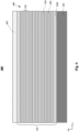
- fabrication process 400 starts at process step S410, where an alternating dielectric stack can be disposed on a substrate.
- An example of a 3D memory device at the process step S410 is shown as a 3D memory structure 500 in Fig. 5 .
- the substrate of the 3D memory structure 500 can be similar to the substrate 330 in Fig. 3 .
- the substrate 330 can provide a platform for forming subsequent structures.
- the substrate 330 can be any suitable semiconductor substrate having any suitable semiconductor materials, such as monocrystalline, polycrystalline or single crystalline semiconductors.
- the substrate 330 can include silicon, silicon germanium (SiGe), germanium (Ge), silicon on insulator (SOI), germanium on insulator (GOI), gallium arsenide (GaAs), gallium nitride, silicon carbide, III-V compound, or any combinations thereof.
- the substrate 330 can include a layer of semiconductor material formed on a handle wafer, for example, glass, plastic, or another semiconductor substrate.
- a front surface 330f of the substrate 330 is also referred to as a "main surface” or a "top surface” of the substrate herein. Layers of materials can be disposed on the front surface 330f of the substrate 330. A “topmost” or “upper” layer is a layer farthest or farther away from the front surface 330f of the substrate. A “bottommost” or “lower” layer is a layer closest or closer to the front surface 330f of the substrate.
- the formation of the alternating dielectric stack 554 can include disposing the first dielectric layers 558 to each have the same thickness or to have different thicknesses.
- Example thicknesses of the first dielectric layers 558 can range from 10 nm to 500 nm, preferably about 25nm.
- the second dielectric layer 560 can each have the same thickness or have different thicknesses.
- Example thicknesses of the second dielectric layer 560 can range from 10 nm to 500 nm, preferably about 35nm. It should be understood that the number of dielectric layer pairs 556 in Fig. 5 is for illustrative purposes only and that any suitable number of layers may be included in the alternating dielectric stack 554.
- the first dielectric layer 558 includes any suitable insulating materials, for example, silicon oxide, silicon oxynitride, silicon nitride, TEOS or silicon oxide with F-, C-, N-, and/or H- incorporation.
- the first dielectric layer 558 can also include high-k dielectric materials, for example, hafnium oxide, zirconium oxide, aluminum oxide, tantalum oxide, or lanthanum oxide films.
- the first dielectric layer 558 can be any combination of the above materials.
- the formation of the first dielectric layer 558 on the substrate 330 can include any suitable deposition methods such as, chemical vapor deposition (CVD), physical vapor deposition (PVD), plasma-enhanced CVD (PECVD), rapid thermal chemical vapor deposition (RTCVD), low pressure chemical vapor deposition (LPCVD), sputtering, metal-organic chemical vapor deposition (MOCVD), atomic layer deposition (ALD), high-density-plasma CVD (HDP-CVD), thermal oxidation, nitridation, any other suitable deposition method, and/or combinations thereof.
- CVD chemical vapor deposition
- PVD physical vapor deposition
- PECVD plasma-enhanced CVD
- RTCVD rapid thermal chemical vapor deposition
- LPCVD low pressure chemical vapor deposition
- sputtering metal-organic chemical vapor deposition
- MOCVD metal-organic chemical vapor deposition
- ALD atomic layer deposition
- HDP-CVD
- the second dielectric layer 560 includes any suitable material that is different from the first dielectric layer 558 and can be removed selectively with respect to the first dielectric layer 558.
- the second dielectric layer 560 can include silicon oxide, silicon oxynitride, silicon nitride, TEOS, poly-crystalline silicon, poly-crystalline germanium, poly-crystalline germanium-silicon, and any combinations thereof.
- the second dielectric layer 560 also includes amorphous semiconductor materials, such as amorphous silicon or amorphous germanium.
- the second dielectric layer 560 can be disposed using a similar technique as the first dielectric layer 558, such as CVD, PVD, ALD, thermal oxidation or nitridation, or any combination thereof.
- the first dielectric layer 558 can be silicon oxide and the second dielectric layer 560 can be silicon nitride.
- the alternating dielectric stack 554 can include layers in addition to the first dielectric layer 558 and the second dielectric layer 560, and can be made of different materials and/or with different thicknesses.
- a thin metal or metal oxide layer such as zirconium oxide (ZrO 2 ), yttrium oxide (Y 2 O 3 ), and aluminum oxide (Al 2 O 3 ), can be disposed on top of the amorphous carbon layer.
- the hard mask 662 can be disposed by LPCVD, RTCVD, PECVD, ALD, PVD, evaporation, sputtering, or any combination thereof.
- Fig. 7 illustrates a 3D memory structure 700, according to some embodiments of the present disclosure.
- the 3D memory structure 700 includes a contact defining mask 764 disposed on the hard mask 662 over the alternating dielectric stack 554.
- the contact defining mask 764 can include a photoresist or carbon-based polymer material, and can be formed using a patterning process such as lithography.
- the contact defining mask 764 defines the location of contact structures for control gates and select gates of a 3D memory device that will be formed in the subsequent processes.
- the contact structures can be similar to the contact structures 214 for the control gate 333, top select gate (TSG) 334 and lower select gate (LSG) 332 shown in Fig. 3 .
- the hard mask openings 866 can be patterned by using a suitable etching process such as wet etching, dry etching, and/or a combination thereof.
- the hard mask 662 can be etched using an anisotropic etching such as a reactive ion etching (RIE) or other dry etching processes.
- RIE reactive ion etching
- the hard mask 662 is silicon oxide.
- the etching of silicon oxide can include RIE using fluorine-based gases such as carbon-fluorine (CF 4 ), hexafluoroethane (C 2 F 6 ), CHF 3 , or C 3 F 6 and/or any other suitable gases.
- the silicon oxide layer can be etched by wet chemistry, such as hydrofluoric acid or a mixture of hydrofluoric acid and ethylene glycol. In some embodiments, a timed-etch approach can be used.
- the hard mask 662 is silicon nitride. In this example, the etching of silicon nitride can include RIE using O 2 , N 2 , CF 4 , NF 3 , Cl 2 , HBr, BCl 3 , and/or combinations thereof. The methods and etchants to pattern the hard mask 662 should not be limited by the embodiments of the present disclosure.
- the contact defining mask 764 in Fig. 7 can be removed by using techniques such as dry etching with O 2 or CF 4 plasma, or wet etching with resist/polymer stripper, for example solvent based chemicals.
- the 3D memory structure 900 includes a first contact mask 968 disposed on the 3D memory structure 800, over at least a portion of the alternating dielectric stack.
- the first contact mask 968 covers half of the hard mask openings 866 and exposes the other half of the hard mask openings 866.
- the first contact mask 968 can include a photoresist or carbon-based polymer material, and can be formed using a patterning process such as lithography.
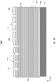
- a first subset of contact openings can be formed in the alternating dielectric stack, according to some embodiments of the present disclosure.
- An exemplary 3D memory device at process step S430 is illustrated as a 3D memory structure 1000 in Fig. 10 .
- the 3D memory structure 1000 includes a first subset of contact openings 1070.
- the first subset of contact openings 1070 can be formed by etching one dielectric layer pair 556 using the first contact mask 968 shown in Fig. 9 .
- the first subset of contact openings 1070 expose a top surface 1070-t of the second dielectric layer pair, where the second dielectric layer pair is located below the first or topmost dielectric layer pair in the alternating dielectric stack 554.
- the dielectric layer pairs are counted sequentially from top to bottom in the alternating dielectric stack 554.
- one or more dielectric layer pairs 556 can be etched with the first contact mask 968.
- the etching process for the first dielectric layer 558 can have a high selectivity over the second dielectric layer 560, and/or vice versa. Accordingly, an underlying dielectric layer pair 556 can function as an etch-stop layer. As a result, multiple dielectric layer pairs 556 can be etched controllably.
- dielectric layer pair 556 can be etched by using an anisotropic etching such as a reactive ion etching (RIE) or other dry etching processes.
- the first dielectric layer 558 is silicon oxide.
- the etching of silicon oxide can include RIE using fluorine-based gases such as carbon-fluorine (CF 4 ), hexafluoroethane (C 2 F 6 ), CHF 3 , or C 3 F 6 and/or any other suitable gases.
- the silicon oxide layer can be etched by wet chemistry, such as hydrofluoric acid or a mixture of hydrofluoric acid and ethylene glycol. In some embodiments, a timed-etch approach can be used.
- half of the hard mask openings 866 can be converted to the first subset of contact openings 1070, with the other half remains as hard mask openings 866. Accordingly, top surfaces of the first and second dielectric layer pairs 866-t and 1070-t can be exposed inside the hard mask openings 866 and the first subset of contact openings 1070, respectively.
- the alternating dielectric stack 554 includes L number of dielectric layer pairs 556.
- the 3D memory structure 800 (in Fig. 8 ) includes N number of hard mask openings 866, wherein the number N is larger or equal to the number L, i.e., N ⁇ L.
- half of the hard mask openings 866 can be converted to the first subset of contact openings 1070.
- the number of first subset of contact openings 1070 can be N/2 and the number of remaining hard mask openings 866 can also be N/2.
- the first subset of contact openings 1070 is not limited as described above and can include any suitable number of the hard mask openings 866.
- a second contact mask can be formed over the alternating dielectric stack, according to some embodiments of the present disclosure.
- An exemplary 3D memory device at process step S435 is illustrated as a 3D memory structure 1100 in Fig. 11 .
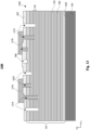
- a second subset of contact openings and a third subset of contact openings can be formed in the alternating dielectric stack, according to some embodiments of the present disclosure.
- An exemplary 3D memory device at process step S440 is illustrated as a 3D memory structure 1200 in Fig. 12 .
- the 3D memory structure 1200 includes a second subset of contact openings 1274 and a third subset of contact openings 1275.
- the second and third subsets of contact openings 1274 can be formed by etching two dielectric layer pairs 556 using the second contact mask 1172 shown in Fig. 11 .
- one or more dielectric layer pairs 556 can be etched with the second contact mask 1172.
- the etching processes for the first and second dielectric layers 558 and 560 can be similar to those used for the first subset of contact openings 1070, where each dielectric layer pair 556 can be etched controllably with an etch-stop on the underlying dielectric layer pair 556.
- the first and second contact masks 968 and 1172 can be designed such that the second subset of contact openings 1274 include half of the first subset of contact openings 1070 and the third subset of contact openings 1275 include half of the remaining hard mask openings 866 that are not converted to the first subset of contact openings 1070 at the process step 430.
- the hard mask openings 866 are formed by etching through the hard mask 662 and the first subset of contact openings 1070 are formed by etching one dielectric layer pair 556, by etching two dielectric layer pair 556 at process step S440
- the second subset of contact openings 1274 can extend through three dielectric layer pairs and expose a top surface 1274-t of the fourth dielectric layer pair.
- the 3D memory structure 1200 can also include some of the first subset of contact openings 1070 extending through one dielectric layer pair 556 and exposing the top surface 1070-t of the second dielectric layer pair.
- the 3D memory structure 1200 can also include some of the hard mask openings 866 extending through the hard mask 662 and exposing the top surface 866-t of the first dielectric layer pair. As illustrated in Fig. 11 , these openings are covered by the second contact mask 1172 at process step S435, and are protected during the etching process of the dielectric layer pairs 556 at process step S440. Therefore, depths of the aforementioned openings are not changed at process step S440.
- the 3D memory structure 1200 can include N/4 number of second subset of contact openings 1274 and N/4 number of third subset of contact openings 1275. In the meantime, there can be N/4 number of first subset of contact openings 1070 and N/4 number of hard mask openings 866 remaining in the 3D memory structure 1200.
- the 3D memory structure 1200 can include different arrangements and depths in the first, second and third subsets of contact openings 1070, 1274 and 1275, as well as the hard mask openings 866.
- a third contact mask is formed over the alternating dielectric stack, according to some embodiments of the present disclosure.
- An exemplary 3D memory device at process step S445 is illustrated as a 3D memory structure 1300 in Fig. 13 .
- a fourth subset, a fifth subset, a sixth subset and a seventh subset of contact openings are formed in the alternating dielectric stack, according to some embodiments of the present disclosure.
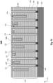
- An exemplary 3D memory device at process step S450 is illustrated as a 3D memory structure 1400 in Fig. 14A .
- the 3D memory structure 1400 includes a fourth subset of contact openings 1478, a fifth subset of contact openings 1479, a sixth subset of contact openings 1480 and a seventh subset of contact openings 1481, formed in the alternating dielectric stack 554, according to some embodiments of the present disclosure.
- the fourth, fifth, sixth and seventh subsets of contact openings 1478-1481 can be formed by etching four dielectric layer pairs 556 using the third contact mask 1376 shown in Fig. 13 .
- one or more dielectric layer pairs 556 can be etched using the third contact mask 1376.
- the etching processes for the first and second dielectric layers 558 and 560 can be similar to those used for the first, second and third subsets of contact openings 1070, 1274 and 1275, where each dielectric layer pair 556 can be etched controllably with an etch-stop on the underlying dielectric layer pair 556.
- a portion of the remaining first subset of contact openings 1070 at process step S440 can be converted to the fifth subset of contact openings 1479 at process step S450.
- a portion of the remaining hard mask openings 866 at process step S430 can be converted to the third subset of contact openings 1275 at process step S440, while a portion of the third subset of contact openings 1275 can be converted to the seventh subset of contact openings 1481 at process step S450.
- a portion of the remaining hard mask openings 866 at process step S440 can be converted to the sixth subset of contact openings 1480 at process step S450.
- the portion of contact openings subjected to the etching of dielectric layer pair 566 at each process step can be any suitable number and is not limited to a half or 50% shown in the Figures 9-13 and 14A .
- the 3D memory structure 1000 can have N/2 number of first subset of contact openings 1070 and N/2 number of hard mask openings 866 after process step S420.
- the 3D memory structure 1200 can have N/4 number of first subset of contact openings 1070, N/4 number of second subset of contact openings 1274, N/4 number of third subset of contact openings 1275, and N/4 number of hard mask openings 866 after process step S440.
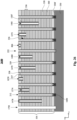
- the filling material 1586 and the liner 1587 can be any suitable material that can be selectively removed over the first dielectric layer 558 and/or second dielectric layer 560 in the subsequent processes.
- the filling material 1586 and the liner 1587 can be an insulator, for example, silicon oxide, silicon oxynitride, silicon nitride, TEOS, amorphous carbon, and/or a combination thereof.
- the filling material 1586 can be silicon nitride and the liner 1587 can be silicon oxide.
- the filling material 1586 and the liner 1587 can be formed by CVD, PVD, sputtering, evaporating, and/or any combination thereof.
- the 3D memory structure 1500 can be planarized after disposing the filling material 1586 and the liner 1587 to form a coplanar top surface.
- a plurality of channel holes can be formed first in the alternating dielectric stack 554, penetrating the entire alternating dielectric stack 554 and extending into the substrate 330.
- forming of the channel holes 336 includes processes such as photolithography and etching.
- a capping layer 1688 formed by a carbon-based polymer material or a hard mask can be used in addition to photoresist for the etching process.
- the capping layer 1688 can include silicon oxide, silicon nitride, TEOS, silicon-containing anti-reflective coating (SiARC), amorphous silicon, or polycrystalline silicon, or any combination thereof.
- the 3D memory structure 1600 further includes an epitaxial layer 1690 inside the channel hole 336.
- the epitaxial layer 1690 can include any suitable semiconductor material, such as silicon, silicon germanium, germanium, gallium arsenide, gallium nitride, III-V compound, or any combination thereof.
- the epitaxial layer 1690 can be epitaxially grown from the substrate 330.
- the epitaxial layer 1690 can be selectively grown from an exposed surface of the substrate 330 inside the channel hole 336.
- the epitaxial layer 1690 can be a polycrystalline semiconductor material, for example, polycrystalline silicon.
- the epitaxial layer 1690 can be epitaxially grown from a doped region (not shown in Fig. 16 ) in the substrate 330.
- the doped region can be formed by ion implantation using p-type or n-type dopants, for example boron, phosphorus, arsenic, or any combination thereof.
- the ion implantation can be performed before the deposition of the alternating dielectric stack 554. In some embodiments, the ion implantation can be performed after channel hole etching.
- a memory film (e.g., the memory film 337 in Fig. 3 ) can be disposed on a sidewall of each channel hole 336, and a top surface of the epitaxial layer 558.
- the memory film 337 can be a composite layer including a tunneling layer, a storage layer (also known as "charge trap/storage layer"), and a blocking layer.
- Each channel hole 336 can have a cylinder shape.
- the tunneling layer, the storage layer, and the blocking layer are arranged along a direction from the center toward the outer of the channel hole in the above order, according to some embodiments.
- the tunneling layer can include silicon oxide, silicon nitride, or any combination thereof.
- the blocking layer can include silicon oxide, silicon nitride, high dielectric constant (high-k) dielectrics, or any combination thereof.
- the storage layer can include silicon nitride, silicon oxynitride, silicon, or any combination thereof.
- the memory film 337 includes ONO dielectrics (e.g., a tunneling layer including silicon oxide, a storage layer including silicon nitride, and a blocking layer including silicon oxide).
- the core filling film 339 can be disposed to fill each channel hole 336.
- the middle of the core filling film 339 can include one or more air gaps.
- the core filling film 339 can be any suitable insulator, for example, silicon oxide, silicon nitride, silicon oxynitride, spin-on-glass, boron or phosphorus doped silicon oxide, carbon-doped oxide (CDO or SiOC or SiOC:H), fluorine doped oxide (SiOF), or any combination thereof.
- the core filling film 339 can be deposited by using, for example, ALD, PVD, CVD, spin-coating, sputtering, or any other suitable film deposition techniques.
- the core filling film 339 can also be formed by using repeated deposition and etch-back processes.
- the etch-back process can include, but not limited to, a wet etching, a dry etching, or a combination thereof.
- the core filling film 339, the channel layer 338 and the capping layer 1688 are can be coplanar in the 3D memory structure 1600.
- the planarization process includes chemical mechanical polishing, RIE, wet etching, or a combination thereof. The planarization process removes excess core filling film 339, channel layer 338 and the memory film 337 outside the channel hole 336. Accordingly, the channel layer 338 and the memory film 337 can be disconnected between adjacent channel holes 336.
- Fig. 17 illustrates a 3D memory structure 1700, according to some embodiments of the present disclosure.
- the 3D memory structure 1700 includes a plurality of slit openings 1792 penetrating through the entire alternating dielectric stack 554.
- the slit openings 1792 can extend laterally along the WL direction in the x-y plane that parallel to the top surface 330f.
- the slit openings 1792 can form slit structures 216 (in Figs. 2 and 3 ) in subsequent fabrication processes.
- the arrangement of the slit openings 1792 in Fig. 17 is only for illustration purpose and is not so limited.
- a film stack of alternating conductive and dielectric layers can be formed, according to some embodiments of the present disclosure.
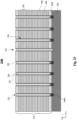
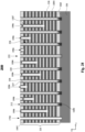
- An exemplary 3D memory device at process step S465 is illustrated as a 3D memory structure 1800 in Fig. 18 .
- the 3D memory structure 1800 includes a film stack of alternating conductive and dielectric layers, similar to the film stack 335 in Fig. 3 .
- the conductive layer 1894 can also be poly-crystalline semiconductors, such as poly-crystalline silicon, poly-crystalline germanium, poly-crystalline germanium-silicon and any other suitable material, and/or combinations thereof.
- the poly-crystalline material can be incorporated with any suitable types of dopant, such as boron, phosphorous, or arsenic.
- the conductive layer 1894 can also be amorphous semiconductors.
- the conductive layer 1894 can be made from a metal silicide, including WSi x , CoSi x , NiSi x , or AlSi x , etc.
- the forming of the metal silicide material can include forming a metal layer and a poly-crystalline semiconductor using similar techniques described above.
- the forming of metal silicide can further include applying a thermal annealing process on the deposited metal layer and the poly-crystalline semiconductor layer, followed by removal of unreacted metal.
- a gate dielectric layer can be disposed in the lateral tunnels prior to the conductive layer 1894 (not shown in Fig. 18 ) to reduce leakage current between adjacent word lines (gate electrodes) and/or to reduce leakage current between gate and channel.
- the gate dielectric layer can include silicon oxide, silicon nitride, silicon oxynitride, and/or any suitable combinations thereof.
- the gate dielectric layer can also include high-k dielectric materials, such as hafnium oxide, zirconium oxide, aluminum oxide, tantalum oxide, lanthanum oxide, and/or any combination thereof.
- the gate dielectric layer can be disposed by one or more suitable deposition processes, such as CVD, PVD, and/or ALD.
- the conductive layers 1894 can function as gate electrodes at the intersection with memory strings 212.
- the ten conductive layers 1894 can form ten gate electrodes for each memory string 212, e.g., TSG 334, LSG 332 and eight control gates 333.
- each memory string 212 can have eight memory cells 340. It is noted that the number of memory strings and memory cells are shown for illustrative purposes in Fig. 18 , and can be increased for higher storage capacity.
- conductive materials inside the slit openings 1792 during deposition can be removed.
- insulating materials can be disposed inside some of the slit openings 1792 to form slit structures 216, separating a memory block into multiple programmable and readable memory fingers (see Fig. 2A-2B).
- Fig. 19 illustrates a 3D memory structure 1900, according to some embodiments of the present disclosure.
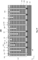
- the 3D memory structure 1900 includes a plurality of contact holes 1996, formed by removing the filling materials 1586 inside the contact fills 1584 in the 3D memory structure 1800 in Fig. 18 .
- the contact holes 1996 can be formed by lithography, wet chemical etch, dry etch, or a combination thereof.
- the contact holes 1996 extend through the capping layer 1688, one or more pairs of conductive layer 1894 and first dielectric layer 558.
- the contact holes 1996 can expose the conductive layer 1894 in the film stack 335.
- the liner 1587 covers a sidewall of each conductive layer 1894 inside each contact hole 1996 and exposes a top surface of a conductive layer 1894 at a bottom of each contact hole 1996.
- an isolation liner 1997 can be formed on a sidewall of the slit opening 1792, where the isolation liner 1997 inside the slit opening 1792 covers a sidewall of each conductive layer 1894 of the film stack 335. In some embodiments, the isolation liner 1997 can also be formed inside the contact hole 1996.
- the isolation liner 1997 can be any suitable insulator, for example, silicon oxide, silicon nitride, silicon oxynitride or any combination thereof.
- a contact structure can be formed to electrically connect with the conductive layer in the film stack of alternating conductive and dielectric layers, according to some embodiments of the present disclosure.
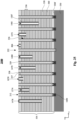
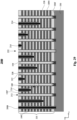
- An exemplary 3D memory device at process step S470 is illustrated as a 3D memory structure 2000 in Fig. 20 .
- the 3D memory structure 2000 includes a plurality of contact structures, similar to the contact structures 214 in Fig. 3 , where the contact structure 214 provides electric connection with the conductive layer 1894 in the film stack 335.
- each contact structure 214 includes a liner surrounding a conductive material.
- the contact structure 214 and the common source contact 2098 can be formed by disposing a conductive material inside the contact hole 1996 and the slit opening 1792.
- the conductive material can include tungsten (W), aluminum (Al), copper (Cu), cobalt (Co), titanium (Ti), tantalum (Ta), titanium nitride (TiN), tantalum nitride (TaN), and/or any combination thereof.
- the conductive material can be disposed by CVD, PVD, PECVD, MOCVD, sputtering, thermal evaporation, e-beam evaporation, ALD, and/or a combination thereof.
- the conductive material can be tungsten (W) deposited by CVD.
- the conductive material used for the contact structure 214 and common source contact 2098 can also be poly-crystalline semiconductors, such as poly-crystalline silicon, poly-crystalline germanium, poly-crystalline germanium-silicon and any other suitable material, and/or combinations thereof.
- the poly-crystalline material can be incorporated with any suitable types of dopant, such as boron, phosphorous, or arsenic.
- the conductive material can also be amorphous semiconductors.
- excess conductive material outside the contact hole 1996 and slit opening 1792 can be removed after the deposition by using an etching process or planarization process.
- the etching process to remove the excess conductive material can include wet chemical etch and/or dry etch (e.g., RIE).
- the planarization process can include chemical mechanical polishing (CMP).
- the contact structures 214 in Fig. 20 and contact holes 1996 in Fig. 19 correspond to the hard mask openings 866 and/or contact openings 1070, 1274-1275, 1478-1481 in Fig. 14A .
- at least one contact opening can be formed for each dielectric layer pair in an alternating dielectric stack with a total 2 ( n-1) number of dielectric layer pairs by using only n number of masks and etching steps.
- at least one contact structure 214 can be formed for each conductive layer 1894 in the film stack 335 without using a staircase structure.
- the contact structures 214 can be formed anywhere in the channel structure region 211 (shown in Fig.
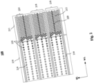
- Figs. 21A-21N provide perspective views of 3D memory structures at various process steps (e.g., process steps S410-S470), showing a different method to form the contact openings, compared with the examples in Figs. 5-13 , 14A-14B and 15-20 .
- process steps S410-S470 e.g., process steps S410-S470
- Detailed description for Figs. 21A-21N is omitted here as the method shown is self-explanatory from these figures and can be understood by a person skilled in the art.
- Fig. 22 illustrates another exemplary fabrication process 2200 for forming a 3D memory device, accordance to some embodiments of the present disclosure.
- Figs. 23-29 illustrate cross-sectional views of the 3D memory device at various process steps according to the fabrication process 2200. It should be understood that the process steps shown in fabrication process 2200 are not exhaustive and that other process steps can be performed as well before, after, or between any of the illustrated process steps. In some embodiments, some process steps of exemplary fabrication process 2200 can be omitted or other process steps can be included, which are not described here for simplicity. In some embodiments, process steps of fabrication process 2200 can be performed in a different order and/or vary.
- fabrication process 2200 starts at process step S2210, where an alternating dielectric stack is disposed on a substrate.
- the exemplary 3D memory structure 500 of a 3D memory device at process step S2210 is shown in Fig. 5 .
- the alternating dielectric stack 554 can include first and second dielectric layers 558 and 560.
- channel holes and memory strings can be formed in the alternating dielectric stack.
- An exemplary 3D memory structure 2300 at process step S2220 is shown in Fig. 23 , where the channel holes 336 and the memory strings 212 are similar to the respective ones in Fig. 16 and can be formed by using similar techniques.
- dummy memory strings similar to the dummy memory strings 222 in Fig. 16 can also be formed by using similar techniques.
- a plurality of contact openings can be formed in the alternating dielectric stack by using multiple contact masks.
- An exemplary 3D memory structure 2400 at process step S2230 is shown in Fig. 24 , where the hard mask openings 866, the first subset of contact openings 1070, the second and third subsets of contact openings 1274-1275, and the fourth to seventh subsets of contact openings 1478-1481 can be similar to the respective ones in Fig. 14A and can be formed by using similar processes in the process steps S415-S450 described in Fig. 4 and Figs. 6-13 and 14A-14B .
- slit openings can be formed in the alternating dielectric stack.
- An exemplary 3D memory structure 2600 at process step S2250 is shown in Fig. 26 , where the slit opening 1792 is similar to the one in Fig. 17 and can be formed using similar techniques.
- a film stack of alternating conductive and dielectric layers can be formed.
- An exemplary 3D memory structure 2700 at process step S2260 is shown in Fig. 27 , where the film stack 335 of alternating conductive and dielectric layers is similar to the one in Fig. 18 and can be formed using similar techniques.
- contact structures can be formed to electrically connect with the conductive layer in the film stack of alternating conductive and dielectric layers.
- An exemplary 3D memory structure 2900 at process step S2270 is shown in Fig. 29 , where the contact structures 214 are similar to the ones in Fig. 20 and can be formed using similar techniques.
- the 3D memory structure 2900 can also include the common source contact 2098, similar to the one in Fig. 20 .
- the third aspect of the present disclosure provides another method for forming a three-dimensional (3D) memory structure that includes disposing an alternating dielectric stack on a substrate, wherein the alternating dielectric stack includes 2 n number of dielectric layer pairs, wherein n is an integer and each dielectric layer pair includes a first dielectric layer and a second dielectric layer that is different from the first dielectric layer.
- the method also includes forming a plurality of contact openings by using ( n +1) cycles of repetitive patterning process.
- An i -th patterning process includes etching 2 ( i - 1) number of dielectric layer pairs such that top 2 i number of dielectric layer pairs are exposed inside the plurality of contact openings, where i is an integer ranging from 1 to n.
Landscapes
- Semiconductor Memories (AREA)
- Non-Volatile Memory (AREA)
- Electrodes Of Semiconductors (AREA)
- Drying Of Semiconductors (AREA)
Priority Applications (1)
| Application Number | Priority Date | Filing Date | Title |
|---|---|---|---|
| EP25158831.5A EP4535953A3 (de) | 2020-03-13 | 2020-03-13 | Kontaktstrukturen für dreidimensionalen speicher |
Applications Claiming Priority (3)
| Application Number | Priority Date | Filing Date | Title |
|---|---|---|---|
| EP20924240.3A EP3928351B1 (de) | 2020-03-13 | 2020-03-13 | Kontaktstrukturen für einen dreidimensionalen speicher |
| EP25158831.5A EP4535953A3 (de) | 2020-03-13 | 2020-03-13 | Kontaktstrukturen für dreidimensionalen speicher |
| PCT/CN2020/079087 WO2021179273A1 (en) | 2020-03-13 | 2020-03-13 | Contact structures for three-dimensional memory |
Related Parent Applications (1)
| Application Number | Title | Priority Date | Filing Date |
|---|---|---|---|
| EP20924240.3A Division EP3928351B1 (de) | 2020-03-13 | 2020-03-13 | Kontaktstrukturen für einen dreidimensionalen speicher |
Publications (2)
| Publication Number | Publication Date |
|---|---|
| EP4535953A2 true EP4535953A2 (de) | 2025-04-09 |
| EP4535953A3 EP4535953A3 (de) | 2025-09-03 |
Family
ID=71657283
Family Applications (2)
| Application Number | Title | Priority Date | Filing Date |
|---|---|---|---|
| EP25158831.5A Pending EP4535953A3 (de) | 2020-03-13 | 2020-03-13 | Kontaktstrukturen für dreidimensionalen speicher |
| EP20924240.3A Active EP3928351B1 (de) | 2020-03-13 | 2020-03-13 | Kontaktstrukturen für einen dreidimensionalen speicher |
Family Applications After (1)
| Application Number | Title | Priority Date | Filing Date |
|---|---|---|---|
| EP20924240.3A Active EP3928351B1 (de) | 2020-03-13 | 2020-03-13 | Kontaktstrukturen für einen dreidimensionalen speicher |
Country Status (7)
| Country | Link |
|---|---|
| US (3) | US11862565B2 (de) |
| EP (2) | EP4535953A3 (de) |
| JP (4) | JP7217365B6 (de) |
| KR (2) | KR20240066294A (de) |
| CN (1) | CN111448648B (de) |
| TW (1) | TWI737279B (de) |
| WO (1) | WO2021179273A1 (de) |
Families Citing this family (29)
| Publication number | Priority date | Publication date | Assignee | Title |
|---|---|---|---|---|
| JP7217365B6 (ja) | 2020-03-13 | 2024-02-08 | 長江存儲科技有限責任公司 | 三次元メモリのためのコンタクト構造 |
| CN113571467B (zh) * | 2020-03-13 | 2024-07-23 | 长江存储科技有限责任公司 | 用于三维存储器的接触结构 |
| WO2021184287A1 (en) * | 2020-03-19 | 2021-09-23 | Yangtze Memory Technologies Co., Ltd. | Method for forming contact structures in three-dimensional memory devices |
| CN112490247B (zh) * | 2020-12-01 | 2022-10-04 | 长江存储科技有限责任公司 | 一种三维存储器及其制备方法 |
| JP2022134165A (ja) | 2021-03-03 | 2022-09-15 | キオクシア株式会社 | 半導体記憶装置 |
| US11917828B2 (en) * | 2021-05-07 | 2024-02-27 | Macronix International Co., Ltd. | Memory devices with multiple string select line cuts |
| CN115360199A (zh) * | 2021-05-17 | 2022-11-18 | 三星电子株式会社 | 三维半导体存储器装置和包括其的电子系统 |
| US11756785B2 (en) * | 2021-08-20 | 2023-09-12 | Applied Materials, Inc. | Molecular layer deposition contact landing protection for 3D NAND |
| WO2023024012A1 (en) * | 2021-08-26 | 2023-03-02 | Yangtze Memory Technologies Co., Ltd. | Three-dimensional nand memory and fabrication method thereof |
| EP4152395A1 (de) * | 2021-09-20 | 2023-03-22 | Fraunhofer-Gesellschaft zur Förderung der angewandten Forschung e.V. | Verfahren zum herstellen eines dreidimensional-integrierten halbleiterspeichers |
| EP4152394A1 (de) | 2021-09-20 | 2023-03-22 | Fraunhofer-Gesellschaft zur Förderung der angewandten Forschung e.V. | Verfahren zum erzeugen von vertikalen kanalstrukturen in dreidimensional integrierten halbleiterspeichern |
| CN113851479B (zh) * | 2021-09-22 | 2025-01-07 | 长江存储科技有限责任公司 | 三维存储器及其制备方法 |
| US11974424B2 (en) * | 2021-11-30 | 2024-04-30 | Winbond Electronics Corp. | Memory device and method of forming the same |
| US20250176187A1 (en) * | 2022-02-24 | 2025-05-29 | Applied Materials, Inc. | Memory device with staircase free structure and methods for forming the same |
| TW202410405A (zh) | 2022-05-16 | 2024-03-01 | 美商應用材料股份有限公司 | 用於3d記憶體之直接字元線觸點與製造方法 |
| CN115020328B (zh) * | 2022-05-27 | 2025-12-19 | 长江存储科技有限责任公司 | 存储器器件的制造方法、存储器器件和存储器系统 |
| EP4367666B1 (de) | 2022-09-23 | 2025-03-26 | Yangtze Memory Technologies Co., Ltd. | Dreidimensionale speichervorrichtungen und verfahren zur formung davon |
| WO2024060218A1 (en) | 2022-09-23 | 2024-03-28 | Yangtze Memory Technologies Co., Ltd. | Three-dimensional memory devices and methods for forming the same |
| WO2024118804A1 (en) * | 2022-12-02 | 2024-06-06 | Applied Materials, Inc. | Wordline contact formation for nand device |
| CN118175848A (zh) * | 2022-12-09 | 2024-06-11 | 长江存储科技有限责任公司 | 半导体器件、制备方法及存储系统 |
| US20240365545A1 (en) * | 2023-04-25 | 2024-10-31 | Applied Materials, Inc. | Wordline contact formation for nand device |
| US20240381639A1 (en) * | 2023-05-10 | 2024-11-14 | Western Digital Technologies, Inc. | Three-dimensional memory device with layer contact via structures located in a memory array region and methods of forming the same |
| US20250079294A1 (en) * | 2023-08-29 | 2025-03-06 | Western Digital Technologies, Inc., | Stairless three-dimensional memory device with layer contact via structures located above support pillar structures and methods of forming the same |
| KR20250043111A (ko) * | 2023-09-21 | 2025-03-28 | 삼성전자주식회사 | 반도체 장치 및 그를 포함하는 데이터 저장 시스템 |
| US20250140688A1 (en) * | 2023-10-26 | 2025-05-01 | Western Digital Technologies, Inc., | Three-dimensional memory device containing dummy via cavities and method for making same |
| KR20250062822A (ko) * | 2023-10-31 | 2025-05-08 | 에스케이하이닉스 주식회사 | 반도체 장치 및 그 제조 방법 |
| CN119947097A (zh) * | 2023-11-02 | 2025-05-06 | 长江存储科技有限责任公司 | 半导体装置、三维存储器装置以及形成其的方法 |
| CN121286111A (zh) * | 2024-04-18 | 2026-01-06 | 长江存储科技有限责任公司 | 三维半导体装置中的触点结构 |
| KR20250170014A (ko) | 2025-11-17 | 2025-12-04 | 삼성전자주식회사 | 반도체 메모리 장치 및 그를 포함하는 전자 시스템 |
Family Cites Families (32)
| Publication number | Priority date | Publication date | Assignee | Title |
|---|---|---|---|---|
| JP2009016400A (ja) | 2007-06-29 | 2009-01-22 | Toshiba Corp | 積層配線構造体及びその製造方法並びに半導体装置及びその製造方法 |
| TWI447851B (zh) * | 2011-01-19 | 2014-08-01 | Macronix Int Co Ltd | 多層連線結構及製造方法 |
| JP2012244180A (ja) | 2011-05-24 | 2012-12-10 | Macronix Internatl Co Ltd | 多層接続構造及びその製造方法 |
| JP2013055136A (ja) | 2011-09-01 | 2013-03-21 | Toshiba Corp | 不揮発性半導体記憶装置及びその製造方法 |
| JP2013187335A (ja) | 2012-03-07 | 2013-09-19 | Toshiba Corp | 半導体装置及びその製造方法 |
| KR101981996B1 (ko) | 2012-06-22 | 2019-05-27 | 에스케이하이닉스 주식회사 | 반도체 소자와 그 제조방법 |
| US8633099B1 (en) | 2012-07-19 | 2014-01-21 | Macronix International Co., Ltd. | Method for forming interlayer connectors in a three-dimensional stacked IC device |
| US9524901B2 (en) * | 2014-09-30 | 2016-12-20 | Sandisk Technologies Llc | Multiheight electrically conductive via contacts for a multilevel interconnect structure |
| US9941209B2 (en) * | 2016-03-11 | 2018-04-10 | Micron Technology, Inc. | Conductive structures, systems and devices including conductive structures and related methods |
| US9754963B1 (en) * | 2016-08-22 | 2017-09-05 | Sandisk Technologies Llc | Multi-tier memory stack structure containing two types of support pillar structures |
| KR102629347B1 (ko) * | 2016-12-08 | 2024-01-26 | 삼성전자주식회사 | 반도체 장치 및 그 제조 방법 |
| US9875929B1 (en) | 2017-01-23 | 2018-01-23 | Sandisk Technologies Llc | Three-dimensional memory device with annular blocking dielectrics and discrete charge storage elements and method of making thereof |
| CN106920794B (zh) | 2017-03-08 | 2018-11-30 | 长江存储科技有限责任公司 | 一种3d nand存储器件及其制造方法 |
| KR20250025029A (ko) * | 2017-03-08 | 2025-02-20 | 양쯔 메모리 테크놀로지스 씨오., 엘티디. | 3차원 메모리 장치의 쓰루 어레이 컨택 구조 |
| KR20180110797A (ko) | 2017-03-30 | 2018-10-11 | 에스케이하이닉스 주식회사 | 반도체 장치 및 그 제조 방법 |
| KR20180138403A (ko) * | 2017-06-21 | 2018-12-31 | 에스케이하이닉스 주식회사 | 반도체 장치 및 그 제조방법 |
| US10438964B2 (en) | 2017-06-26 | 2019-10-08 | Sandisk Technologies Llc | Three-dimensional memory device having direct source contact and metal oxide blocking dielectric and method of making thereof |
| KR102373818B1 (ko) | 2017-07-18 | 2022-03-14 | 삼성전자주식회사 | 반도체 장치 |
| JP6863864B2 (ja) * | 2017-09-08 | 2021-04-21 | キオクシア株式会社 | 記憶装置 |
| JP2019057623A (ja) | 2017-09-21 | 2019-04-11 | 東芝メモリ株式会社 | 積層配線構造体及び積層配線構造体の製造方法 |
| US10373969B2 (en) * | 2018-01-09 | 2019-08-06 | Sandisk Technologies Llc | Three-dimensional memory device including partially surrounding select gates and fringe field assisted programming thereof |
| US10763271B2 (en) | 2018-06-27 | 2020-09-01 | Sandisk Technologies Llc | Three-dimensional memory device containing aluminum-silicon word lines and methods of manufacturing the same |
| CN109155319B (zh) * | 2018-08-08 | 2019-09-10 | 长江存储科技有限责任公司 | 存储器件以及形成存储器件的方法 |
| US10580791B1 (en) * | 2018-08-21 | 2020-03-03 | Micron Technology, Inc. | Semiconductor device structures, semiconductor devices, and electronic systems |
| KR102935787B1 (ko) * | 2018-09-26 | 2026-03-05 | 양쯔 메모리 테크놀로지스 씨오., 엘티디. | 3d 메모리 장치 및 3d 메모리 장치 형성 방법 |
| CN109524417B (zh) * | 2018-11-27 | 2021-03-30 | 长江存储科技有限责任公司 | 3d nand存储器及其形成方法 |
| CN109716521A (zh) * | 2018-12-12 | 2019-05-03 | 长江存储科技有限责任公司 | 用于三维存储器件的接触结构 |
| KR102747577B1 (ko) * | 2018-12-21 | 2025-01-02 | 삼성전자주식회사 | 3차원 반도체 메모리 소자 |
| US11563022B2 (en) * | 2019-08-25 | 2023-01-24 | Micron Technology, Inc. | Memory arrays and methods used in forming a memory array comprising strings of memory cells |
| WO2021035603A1 (en) * | 2019-08-29 | 2021-03-04 | Yangtze Memory Technologies Co., Ltd. | Three-dimensional memory and fabrication method thereof |
| WO2021051383A1 (en) | 2019-09-20 | 2021-03-25 | Yangtze Memory Technologies Co., Ltd. | Three-dimensional memory device having multi-deck structure and methods for forming the same |
| JP7217365B6 (ja) | 2020-03-13 | 2024-02-08 | 長江存儲科技有限責任公司 | 三次元メモリのためのコンタクト構造 |
-
2020
- 2020-03-13 JP JP2021561769A patent/JP7217365B6/ja active Active
- 2020-03-13 CN CN202080000523.XA patent/CN111448648B/zh active Active
- 2020-03-13 KR KR1020247014403A patent/KR20240066294A/ko active Pending
- 2020-03-13 KR KR1020217033137A patent/KR102663224B1/ko active Active
- 2020-03-13 EP EP25158831.5A patent/EP4535953A3/de active Pending
- 2020-03-13 WO PCT/CN2020/079087 patent/WO2021179273A1/en not_active Ceased
- 2020-03-13 EP EP20924240.3A patent/EP3928351B1/de active Active
- 2020-04-28 TW TW109114184A patent/TWI737279B/zh active
- 2020-05-15 US US16/875,180 patent/US11862565B2/en active Active
-
2022
- 2022-01-13 US US17/575,158 patent/US20220139837A1/en not_active Abandoned
-
2023
- 2023-01-23 JP JP2023008085A patent/JP7585362B2/ja active Active
-
2024
- 2024-11-01 JP JP2024193118A patent/JP7787272B2/ja active Active
-
2025
- 2025-02-05 US US19/046,199 patent/US20250183177A1/en active Pending
- 2025-12-03 JP JP2025227093A patent/JP2026040491A/ja active Pending
Also Published As
| Publication number | Publication date |
|---|---|
| KR20210141561A (ko) | 2021-11-23 |
| TWI737279B (zh) | 2021-08-21 |
| CN111448648B (zh) | 2021-06-08 |
| EP3928351B1 (de) | 2025-02-26 |
| JP7787272B2 (ja) | 2025-12-16 |
| CN111448648A (zh) | 2020-07-24 |
| US20250183177A1 (en) | 2025-06-05 |
| KR20240066294A (ko) | 2024-05-14 |
| US20210287991A1 (en) | 2021-09-16 |
| JP7217365B6 (ja) | 2024-02-08 |
| JP2026040491A (ja) | 2026-03-09 |
| JP2022529163A (ja) | 2022-06-17 |
| JP7217365B2 (ja) | 2023-02-02 |
| EP3928351A4 (de) | 2023-02-01 |
| JP7585362B2 (ja) | 2024-11-18 |
| EP3928351A1 (de) | 2021-12-29 |
| TW202135237A (zh) | 2021-09-16 |
| WO2021179273A1 (en) | 2021-09-16 |
| EP4535953A3 (de) | 2025-09-03 |
| JP2023038292A (ja) | 2023-03-16 |
| US20220139837A1 (en) | 2022-05-05 |
| JP2025014056A (ja) | 2025-01-28 |
| US11862565B2 (en) | 2024-01-02 |
| KR102663224B1 (ko) | 2024-05-03 |
Similar Documents
| Publication | Publication Date | Title |
|---|---|---|
| EP3928351B1 (de) | Kontaktstrukturen für einen dreidimensionalen speicher | |
| US11910599B2 (en) | Contact structures for three-dimensional memory device | |
| US20240324224A1 (en) | Three-dimensional memory and fabrication method thereof | |
| US20230335170A1 (en) | Staircase bridge structures for word line contacts in three-dimensional memory | |
| US11107834B2 (en) | Staircase and contact structures for three-dimensional memory | |
| US20240431111A1 (en) | Bottom select gate contacts for center staircase structures in three-dimensional memory devices | |
| US11456315B2 (en) | Dual deck three-dimensional NAND memory with channel dips and method for forming the same | |
| US20250323159A1 (en) | Three-dimensional nand memory and fabrication method thereof | |
| CN113571467B (zh) | 用于三维存储器的接触结构 |
Legal Events
| Date | Code | Title | Description |
|---|---|---|---|
| PUAI | Public reference made under article 153(3) epc to a published international application that has entered the european phase |
Free format text: ORIGINAL CODE: 0009012 |
|
| STAA | Information on the status of an ep patent application or granted ep patent |
Free format text: STATUS: REQUEST FOR EXAMINATION WAS MADE |
|
| 17P | Request for examination filed |
Effective date: 20250219 |
|
| AC | Divisional application: reference to earlier application |
Ref document number: 3928351 Country of ref document: EP Kind code of ref document: P |
|
| AK | Designated contracting states |
Kind code of ref document: A2 Designated state(s): AL AT BE BG CH CY CZ DE DK EE ES FI FR GB GR HR HU IE IS IT LI LT LU LV MC MK MT NL NO PL PT RO RS SE SI SK SM TR |
|
| REG | Reference to a national code |
Ref country code: DE Ref legal event code: R079 Free format text: PREVIOUS MAIN CLASS: H10B0043500000 Ipc: H10B0043100000 |
|
| PUAL | Search report despatched |
Free format text: ORIGINAL CODE: 0009013 |
|
| AK | Designated contracting states |
Kind code of ref document: A3 Designated state(s): AL AT BE BG CH CY CZ DE DK EE ES FI FR GB GR HR HU IE IS IT LI LT LU LV MC MK MT NL NO PL PT RO RS SE SI SK SM TR |
|
| RIC1 | Information provided on ipc code assigned before grant |
Ipc: H10B 43/10 20230101AFI20250725BHEP Ipc: H10B 43/27 20230101ALI20250725BHEP Ipc: H10B 43/50 20230101ALI20250725BHEP Ipc: H01L 21/768 20060101ALN20250725BHEP |