JP2012244180A - 多層接続構造及びその製造方法 - Google Patents
多層接続構造及びその製造方法 Download PDFInfo
- Publication number
- JP2012244180A JP2012244180A JP2012115192A JP2012115192A JP2012244180A JP 2012244180 A JP2012244180 A JP 2012244180A JP 2012115192 A JP2012115192 A JP 2012115192A JP 2012115192 A JP2012115192 A JP 2012115192A JP 2012244180 A JP2012244180 A JP 2012244180A
- Authority
- JP
- Japan
- Prior art keywords
- contact
- mask
- level
- opening
- levels
- Prior art date
- Legal status (The legal status is an assumption and is not a legal conclusion. Google has not performed a legal analysis and makes no representation as to the accuracy of the status listed.)
- Pending
Links
Images


Classifications
-
- H—ELECTRICITY
- H01—ELECTRIC ELEMENTS
- H01L—SEMICONDUCTOR DEVICES NOT COVERED BY CLASS H10
- H01L28/00—Passive two-terminal components without a potential-jump or surface barrier for integrated circuits; Details thereof; Multistep manufacturing processes therefor
- H01L28/40—Capacitors
- H01L28/60—Electrodes
- H01L28/82—Electrodes with an enlarged surface, e.g. formed by texturisation
- H01L28/90—Electrodes with an enlarged surface, e.g. formed by texturisation having vertical extensions
-
- H—ELECTRICITY
- H01—ELECTRIC ELEMENTS
- H01L—SEMICONDUCTOR DEVICES NOT COVERED BY CLASS H10
- H01L27/00—Devices consisting of a plurality of semiconductor or other solid-state components formed in or on a common substrate
- H01L27/02—Devices consisting of a plurality of semiconductor or other solid-state components formed in or on a common substrate including semiconductor components specially adapted for rectifying, oscillating, amplifying or switching and having at least one potential-jump barrier or surface barrier; including integrated passive circuit elements with at least one potential-jump barrier or surface barrier
- H01L27/0203—Particular design considerations for integrated circuits
- H01L27/0207—Geometrical layout of the components, e.g. computer aided design; custom LSI, semi-custom LSI, standard cell technique
-
- H—ELECTRICITY
- H01—ELECTRIC ELEMENTS
- H01L—SEMICONDUCTOR DEVICES NOT COVERED BY CLASS H10
- H01L27/00—Devices consisting of a plurality of semiconductor or other solid-state components formed in or on a common substrate
- H01L27/02—Devices consisting of a plurality of semiconductor or other solid-state components formed in or on a common substrate including semiconductor components specially adapted for rectifying, oscillating, amplifying or switching and having at least one potential-jump barrier or surface barrier; including integrated passive circuit elements with at least one potential-jump barrier or surface barrier
- H01L27/04—Devices consisting of a plurality of semiconductor or other solid-state components formed in or on a common substrate including semiconductor components specially adapted for rectifying, oscillating, amplifying or switching and having at least one potential-jump barrier or surface barrier; including integrated passive circuit elements with at least one potential-jump barrier or surface barrier the substrate being a semiconductor body
- H01L27/06—Devices consisting of a plurality of semiconductor or other solid-state components formed in or on a common substrate including semiconductor components specially adapted for rectifying, oscillating, amplifying or switching and having at least one potential-jump barrier or surface barrier; including integrated passive circuit elements with at least one potential-jump barrier or surface barrier the substrate being a semiconductor body including a plurality of individual components in a non-repetitive configuration
- H01L27/0611—Devices consisting of a plurality of semiconductor or other solid-state components formed in or on a common substrate including semiconductor components specially adapted for rectifying, oscillating, amplifying or switching and having at least one potential-jump barrier or surface barrier; including integrated passive circuit elements with at least one potential-jump barrier or surface barrier the substrate being a semiconductor body including a plurality of individual components in a non-repetitive configuration integrated circuits having a two-dimensional layout of components without a common active region
- H01L27/0617—Devices consisting of a plurality of semiconductor or other solid-state components formed in or on a common substrate including semiconductor components specially adapted for rectifying, oscillating, amplifying or switching and having at least one potential-jump barrier or surface barrier; including integrated passive circuit elements with at least one potential-jump barrier or surface barrier the substrate being a semiconductor body including a plurality of individual components in a non-repetitive configuration integrated circuits having a two-dimensional layout of components without a common active region comprising components of the field-effect type
- H01L27/0629—Devices consisting of a plurality of semiconductor or other solid-state components formed in or on a common substrate including semiconductor components specially adapted for rectifying, oscillating, amplifying or switching and having at least one potential-jump barrier or surface barrier; including integrated passive circuit elements with at least one potential-jump barrier or surface barrier the substrate being a semiconductor body including a plurality of individual components in a non-repetitive configuration integrated circuits having a two-dimensional layout of components without a common active region comprising components of the field-effect type in combination with diodes, or resistors, or capacitors
-
- H—ELECTRICITY
- H01—ELECTRIC ELEMENTS
- H01L—SEMICONDUCTOR DEVICES NOT COVERED BY CLASS H10
- H01L28/00—Passive two-terminal components without a potential-jump or surface barrier for integrated circuits; Details thereof; Multistep manufacturing processes therefor
- H01L28/40—Capacitors
- H01L28/60—Electrodes
-
- H—ELECTRICITY
- H10—SEMICONDUCTOR DEVICES; ELECTRIC SOLID-STATE DEVICES NOT OTHERWISE PROVIDED FOR
- H10B—ELECTRONIC MEMORY DEVICES
- H10B41/00—Electrically erasable-and-programmable ROM [EEPROM] devices comprising floating gates
- H10B41/20—Electrically erasable-and-programmable ROM [EEPROM] devices comprising floating gates characterised by three-dimensional arrangements, e.g. with cells on different height levels
- H10B41/23—Electrically erasable-and-programmable ROM [EEPROM] devices comprising floating gates characterised by three-dimensional arrangements, e.g. with cells on different height levels with source and drain on different levels, e.g. with sloping channels
- H10B41/27—Electrically erasable-and-programmable ROM [EEPROM] devices comprising floating gates characterised by three-dimensional arrangements, e.g. with cells on different height levels with source and drain on different levels, e.g. with sloping channels the channels comprising vertical portions, e.g. U-shaped channels
-
- H—ELECTRICITY
- H10—SEMICONDUCTOR DEVICES; ELECTRIC SOLID-STATE DEVICES NOT OTHERWISE PROVIDED FOR
- H10B—ELECTRONIC MEMORY DEVICES
- H10B41/00—Electrically erasable-and-programmable ROM [EEPROM] devices comprising floating gates
- H10B41/40—Electrically erasable-and-programmable ROM [EEPROM] devices comprising floating gates characterised by the peripheral circuit region
-
- H—ELECTRICITY
- H10—SEMICONDUCTOR DEVICES; ELECTRIC SOLID-STATE DEVICES NOT OTHERWISE PROVIDED FOR
- H10B—ELECTRONIC MEMORY DEVICES
- H10B41/00—Electrically erasable-and-programmable ROM [EEPROM] devices comprising floating gates
- H10B41/50—Electrically erasable-and-programmable ROM [EEPROM] devices comprising floating gates characterised by the boundary region between the core region and the peripheral circuit region
-
- H—ELECTRICITY
- H10—SEMICONDUCTOR DEVICES; ELECTRIC SOLID-STATE DEVICES NOT OTHERWISE PROVIDED FOR
- H10B—ELECTRONIC MEMORY DEVICES
- H10B43/00—EEPROM devices comprising charge-trapping gate insulators
- H10B43/20—EEPROM devices comprising charge-trapping gate insulators characterised by three-dimensional arrangements, e.g. with cells on different height levels
- H10B43/23—EEPROM devices comprising charge-trapping gate insulators characterised by three-dimensional arrangements, e.g. with cells on different height levels with source and drain on different levels, e.g. with sloping channels
- H10B43/27—EEPROM devices comprising charge-trapping gate insulators characterised by three-dimensional arrangements, e.g. with cells on different height levels with source and drain on different levels, e.g. with sloping channels the channels comprising vertical portions, e.g. U-shaped channels
-
- H—ELECTRICITY
- H10—SEMICONDUCTOR DEVICES; ELECTRIC SOLID-STATE DEVICES NOT OTHERWISE PROVIDED FOR
- H10B—ELECTRONIC MEMORY DEVICES
- H10B43/00—EEPROM devices comprising charge-trapping gate insulators
- H10B43/40—EEPROM devices comprising charge-trapping gate insulators characterised by the peripheral circuit region
-
- H—ELECTRICITY
- H10—SEMICONDUCTOR DEVICES; ELECTRIC SOLID-STATE DEVICES NOT OTHERWISE PROVIDED FOR
- H10B—ELECTRONIC MEMORY DEVICES
- H10B43/00—EEPROM devices comprising charge-trapping gate insulators
- H10B43/50—EEPROM devices comprising charge-trapping gate insulators characterised by the boundary region between the core and peripheral circuit regions
Abstract
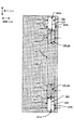
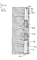
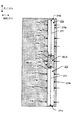
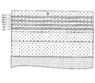
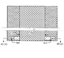
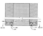
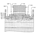
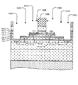
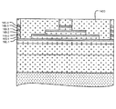
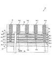
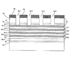
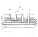
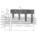
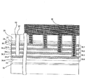
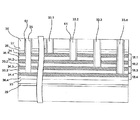
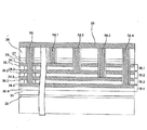
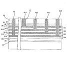
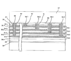
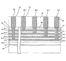
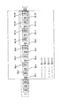
【解決手段】各コンタクトレベルは導電層と絶縁層とを有する。コンタクト開口を作り出すために、第1のコンタクトレベルを露出させるように上部層の一部が除去される。N個のマスクを用いて、最大2N個のコンタクトレベルまでコンタクト開口がエッチングされる。各マスクは、コンタクト開口のうちの実効的に半数をエッチングするために使用される。Nが3であるとき、第1のマスクにより1つのコンタクトレベルがエッチングされ、第2のマスクにより2つのコンタクトレベルがエッチングされ、第3のマスクにより4つのコンタクトレベルがエッチングされる。コンタクト開口の側壁に誘電体層が形成され得る。コンタクト開口内に導電体が形成され、前記誘電体層が該導電体を前記側壁から電気的に絶縁する。
【選択図】図17
Description
Claims (16)
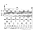
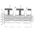
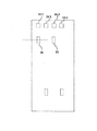
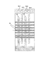
- 相互接続領域に少なくとも4つのコンタクトレベルのスタックを有する3次元積層ICデバイスで使用され、前記コンタクトレベルのランドエリアにアライメントされ且つ該ランドエリアを露出させる相互接続コンタクト領域を形成する方法であって、各コンタクトレベルは導電層と絶縁層とを有し、当該方法は:
各コンタクトレベルのためのコンタクト開口を作り出すために、第1のコンタクトレベルを露出させるように、前記相互接続領域の上に位置する上部層の少なくとも一部を除去するステップと、
Nは2以上の整数として、前記コンタクトレベルの前記スタックに複数レベルの相互接続コンタクト領域を作り出すためのN個のエッチングマスクの組を選定するステップと、
前記N個のマスクを使用して、前記コンタクト開口を最大2N個のコンタクトレベルまでエッチングするステップであり:
第1のマスクを使用して、前記コンタクト開口のうちの実効的に半数で、1つのコンタクトレベルをエッチングするステップ;
第2のマスクを使用して、前記コンタクト開口のうちの実効的に半数で、2つのコンタクトレベルをエッチングするステップ;及び
前記コンタクト開口が前記2N個のコンタクトレベルまで延在するよう、前記除去するステップ、前記選定するステップ及び前記使用するステップを実行するステップ;
を有するステップと、
を有し、
それにより、前記コンタクト開口を通って前記コンタクトレベルの前記ランドエリアに接触する導電体を形成することが可能にされる、
方法。 - 前記除去するステップは、更なるマスクを用いて実行される、請求項1に記載の方法。
- 前記第1のマスクを使用するステップは、前記第1のマスクを用いて1つおきのコンタクト開口で、1つのコンタクトレベルをエッチングすることを有し、
前記第2のマスクを使用するステップは、前記第2のマスクを用いて、少なくとも一組の第1乃至第4のコンタクト開口のうちの第3及び第4のコンタクト開口で、2つのコンタクトレベルをエッチングすることを有する、
請求項1に記載の方法。 - 前記N個のマスクを使用するステップは更に:
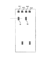
第3のマスクを使用して、前記コンタクト開口のうちの実効的に半数で、4つのコンタクトレベルをエッチングするステップ;及び
第4のマスクを使用して、前記コンタクト開口のうちの実効的に半数で、8つのコンタクトレベルをエッチングするステップ;
を有する、請求項1に記載の方法。 - 前記第3のマスクを使用するステップは、前記第3のマスクを用いて、少なくとも一組の第1乃至第8のコンタクト開口のうちの第5乃至第8のコンタクト開口で、4つのコンタクトレベルをエッチングすることを有し、
前記第4のマスクを使用するステップは、前記第4のマスクを用いて、少なくとも一組の第1乃至第16のコンタクト開口のうちの第9乃至第16のコンタクト開口で、8つのコンタクトレベルをエッチングすることを有する、
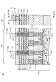
請求項4に記載の方法。 - 前記第1のマスクを使用するステップは、コンタクト開口2、4、6、8、10、12、14、16で1つのコンタクトレベルをエッチングするように実行され、
前記第2のマスクを使用するステップは、コンタクト開口3、4、7、8、11、12、15、16で2つのコンタクトレベルをエッチングするように実行され、
前記第3のマスクを使用するステップは、コンタクト開口5−8、13−16で4つのコンタクトレベルをエッチングするように実行され、
前記第4のマスクを使用するステップは、コンタクト開口9−16で8つのコンタクトレベルをエッチングするように実行される、
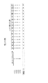
請求項4に記載の方法。 - 前記第1のマスクを使用するステップは、コンタクト開口2、4、6、8、10、12、14、16で8つのコンタクトレベルをエッチングするように実行され、
前記第2のマスクを使用するステップは、コンタクト開口5、6、7、8、13、14、15、16で2つのコンタクトレベルをエッチングするように実行され、
前記第3のマスクを使用するステップは、コンタクト開口3、4、7、8、11、12、15、16で4つのコンタクトレベルをエッチングするように実行され、
前記第4のマスクを使用するステップは、コンタクト開口9−16で1つのコンタクトレベルをエッチングするように実行される、
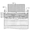
請求項4に記載の方法。 - 前記コンタクトレベルを貫通するグランドコンタクト開口を作り出すステップと、
前記コンタクトレベルの複数の前記導電層と電気的に接触するように、前記グランドコンタクト開口内にグランド導電体を形成するステップと、
を更に有する請求項1に記載の方法。 - 前記グランドコンタクト開口はグランドコンタクト開口側壁を有し、当該方法は更に:
前記グランド導電体が前記グランド導電体と前記コンタクトレベルの前記複数の前記導電層との間に強化された電気接触を生成するように、前記グランド導電体を形成するステップに先立って、前記グランドコンタクト開口側壁において前記絶縁層の一部を除去するステップ、
を更に有する請求項8に記載の方法。 - 前記使用するステップは、エッチングされるコンタクトレベルの数順とは異なる順序で実行される、請求項1に記載の方法。
- 前記コンタクト開口は側壁を有し、当該方法は更に、該側壁に誘電体層を形成するステップを有する、請求項1に記載の方法。
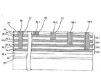
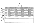
- 相互接続領域の、少なくとも第1、第2、第3及び第4のコンタクトレベルのスタックであり、各コンタクトレベルが導電層と絶縁層とを有する、スタックと、
前記コンタクトレベルのスタックの一部を貫通する第1、第2、第3及び第4の導電体であり、それぞれ、前記第1、第2、第3及び第4のコンタクトレベルの前記導電層と電気的に接触する第1、第2、第3及び第4の導電体と、
前記第2、第3及び第4の導電体がそれぞれ前記第2、第3及び第4の導電層とのみ電気的に接触するように、前記第2、第3及び第4の導電体の周囲を取り囲む誘電体側壁スペーサと、
を有する3次元積層ICデバイス。 - 前記第1、第2、第3及び第4の導電体は一定のピッチを有する、請求項12に記載の積層ICデバイス。
- 前記第1、第2、第3及び第4の導電体の位置は、共通マスクによって決定可能である、請求項12又は13に記載の積層ICデバイス。
- 前記コンタクトレベルのスタックの一部を貫通し且つ前記第1、第2、第3及び第4のコンタクトレベルの前記導電層の各々と電気的に接触するグランド導電体、を更に有する請求項12に記載の積層ICデバイス。
- 前記第1、第2、第3及び第4の導電体並びに前記グランド導電体の位置は、共通マスクによって決定可能である、請求項15に記載の積層ICデバイス。
Applications Claiming Priority (2)
| Application Number | Priority Date | Filing Date | Title |
|---|---|---|---|
| US13/114,931 US8383512B2 (en) | 2011-01-19 | 2011-05-24 | Method for making multilayer connection structure |
| US13/114,931 | 2011-05-24 |
Publications (2)
| Publication Number | Publication Date |
|---|---|
| JP2012244180A true JP2012244180A (ja) | 2012-12-10 |
| JP2012244180A5 JP2012244180A5 (ja) | 2014-07-17 |
Family
ID=47470261
Family Applications (1)
| Application Number | Title | Priority Date | Filing Date |
|---|---|---|---|
| JP2012115192A Pending JP2012244180A (ja) | 2011-05-24 | 2012-05-21 | 多層接続構造及びその製造方法 |
Country Status (4)
| Country | Link |
|---|---|
| US (3) | US20160365407A1 (ja) |
| JP (1) | JP2012244180A (ja) |
| CN (1) | CN106252353B (ja) |
| TW (1) | TWI566447B (ja) |
Cited By (6)
| Publication number | Priority date | Publication date | Assignee | Title |
|---|---|---|---|---|
| US9646987B2 (en) | 2015-06-03 | 2017-05-09 | Kabushiki Kaisha Toshiba | Semiconductor memory device and production method thereof |
| JP2017084849A (ja) * | 2015-10-22 | 2017-05-18 | ラピスセミコンダクタ株式会社 | 半導体装置及び半導体装置の製造方法 |
| US10559533B2 (en) | 2017-09-07 | 2020-02-11 | Toshiba Memory Corporation | Semiconductor device and method of manufacturing the same |
| US10586804B2 (en) | 2017-09-21 | 2020-03-10 | Toshiba Memory Corporation | Multi-layer wiring structure, method for manufacturing multi-layer wiring structure, and semiconductor device |
| JP2022529163A (ja) * | 2020-03-13 | 2022-06-17 | 長江存儲科技有限責任公司 | 三次元メモリのためのコンタクト構造 |
| US11792989B2 (en) | 2017-03-07 | 2023-10-17 | Yangtze Memory Technologies Co., Ltd. | Word line structure of three-dimensional memory device |
Families Citing this family (285)
| Publication number | Priority date | Publication date | Assignee | Title |
|---|---|---|---|---|
| US9394608B2 (en) | 2009-04-06 | 2016-07-19 | Asm America, Inc. | Semiconductor processing reactor and components thereof |
| US8802201B2 (en) | 2009-08-14 | 2014-08-12 | Asm America, Inc. | Systems and methods for thin-film deposition of metal oxides using excited nitrogen-oxygen species |
| US9312155B2 (en) | 2011-06-06 | 2016-04-12 | Asm Japan K.K. | High-throughput semiconductor-processing apparatus equipped with multiple dual-chamber modules |
| US10854498B2 (en) | 2011-07-15 | 2020-12-01 | Asm Ip Holding B.V. | Wafer-supporting device and method for producing same |
| US20130023129A1 (en) | 2011-07-20 | 2013-01-24 | Asm America, Inc. | Pressure transmitter for a semiconductor processing environment |
| US9017481B1 (en) | 2011-10-28 | 2015-04-28 | Asm America, Inc. | Process feed management for semiconductor substrate processing |
| US10714315B2 (en) | 2012-10-12 | 2020-07-14 | Asm Ip Holdings B.V. | Semiconductor reaction chamber showerhead |
| US10683571B2 (en) | 2014-02-25 | 2020-06-16 | Asm Ip Holding B.V. | Gas supply manifold and method of supplying gases to chamber using same |
| US10167557B2 (en) | 2014-03-18 | 2019-01-01 | Asm Ip Holding B.V. | Gas distribution system, reactor including the system, and methods of using the same |
| US11015245B2 (en) | 2014-03-19 | 2021-05-25 | Asm Ip Holding B.V. | Gas-phase reactor and system having exhaust plenum and components thereof |
| US10858737B2 (en) | 2014-07-28 | 2020-12-08 | Asm Ip Holding B.V. | Showerhead assembly and components thereof |
| US9890456B2 (en) | 2014-08-21 | 2018-02-13 | Asm Ip Holding B.V. | Method and system for in situ formation of gas-phase compounds |
| US10941490B2 (en) | 2014-10-07 | 2021-03-09 | Asm Ip Holding B.V. | Multiple temperature range susceptor, assembly, reactor and system including the susceptor, and methods of using the same |
| US9657845B2 (en) | 2014-10-07 | 2017-05-23 | Asm Ip Holding B.V. | Variable conductance gas distribution apparatus and method |
| US10276355B2 (en) | 2015-03-12 | 2019-04-30 | Asm Ip Holding B.V. | Multi-zone reactor, system including the reactor, and method of using the same |
| JP2016225614A (ja) * | 2015-05-26 | 2016-12-28 | 株式会社半導体エネルギー研究所 | 半導体装置 |
| US10458018B2 (en) | 2015-06-26 | 2019-10-29 | Asm Ip Holding B.V. | Structures including metal carbide material, devices including the structures, and methods of forming same |
| US10600673B2 (en) | 2015-07-07 | 2020-03-24 | Asm Ip Holding B.V. | Magnetic susceptor to baseplate seal |
| US10211308B2 (en) | 2015-10-21 | 2019-02-19 | Asm Ip Holding B.V. | NbMC layers |
| US11139308B2 (en) | 2015-12-29 | 2021-10-05 | Asm Ip Holding B.V. | Atomic layer deposition of III-V compounds to form V-NAND devices |
| US10529554B2 (en) | 2016-02-19 | 2020-01-07 | Asm Ip Holding B.V. | Method for forming silicon nitride film selectively on sidewalls or flat surfaces of trenches |
| US10865475B2 (en) | 2016-04-21 | 2020-12-15 | Asm Ip Holding B.V. | Deposition of metal borides and silicides |
| US10190213B2 (en) | 2016-04-21 | 2019-01-29 | Asm Ip Holding B.V. | Deposition of metal borides |
| US10032628B2 (en) | 2016-05-02 | 2018-07-24 | Asm Ip Holding B.V. | Source/drain performance through conformal solid state doping |
| US10367080B2 (en) | 2016-05-02 | 2019-07-30 | Asm Ip Holding B.V. | Method of forming a germanium oxynitride film |
| US11453943B2 (en) | 2016-05-25 | 2022-09-27 | Asm Ip Holding B.V. | Method for forming carbon-containing silicon/metal oxide or nitride film by ALD using silicon precursor and hydrocarbon precursor |
| US9859151B1 (en) | 2016-07-08 | 2018-01-02 | Asm Ip Holding B.V. | Selective film deposition method to form air gaps |
| US10612137B2 (en) | 2016-07-08 | 2020-04-07 | Asm Ip Holdings B.V. | Organic reactants for atomic layer deposition |
| US10714385B2 (en) | 2016-07-19 | 2020-07-14 | Asm Ip Holding B.V. | Selective deposition of tungsten |
| US9812320B1 (en) | 2016-07-28 | 2017-11-07 | Asm Ip Holding B.V. | Method and apparatus for filling a gap |
| KR102532607B1 (ko) | 2016-07-28 | 2023-05-15 | 에이에스엠 아이피 홀딩 비.브이. | 기판 가공 장치 및 그 동작 방법 |
| US9887082B1 (en) | 2016-07-28 | 2018-02-06 | Asm Ip Holding B.V. | Method and apparatus for filling a gap |
| US10643826B2 (en) | 2016-10-26 | 2020-05-05 | Asm Ip Holdings B.V. | Methods for thermally calibrating reaction chambers |
| US11532757B2 (en) | 2016-10-27 | 2022-12-20 | Asm Ip Holding B.V. | Deposition of charge trapping layers |
| US10714350B2 (en) | 2016-11-01 | 2020-07-14 | ASM IP Holdings, B.V. | Methods for forming a transition metal niobium nitride film on a substrate by atomic layer deposition and related semiconductor device structures |
| US10229833B2 (en) | 2016-11-01 | 2019-03-12 | Asm Ip Holding B.V. | Methods for forming a transition metal nitride film on a substrate by atomic layer deposition and related semiconductor device structures |
| US10643904B2 (en) | 2016-11-01 | 2020-05-05 | Asm Ip Holdings B.V. | Methods for forming a semiconductor device and related semiconductor device structures |
| US10134757B2 (en) | 2016-11-07 | 2018-11-20 | Asm Ip Holding B.V. | Method of processing a substrate and a device manufactured by using the method |
| KR102546317B1 (ko) | 2016-11-15 | 2023-06-21 | 에이에스엠 아이피 홀딩 비.브이. | 기체 공급 유닛 및 이를 포함하는 기판 처리 장치 |
| KR102551799B1 (ko) * | 2016-12-06 | 2023-07-05 | 삼성전자주식회사 | 반도체 소자 |
| KR20180068582A (ko) | 2016-12-14 | 2018-06-22 | 에이에스엠 아이피 홀딩 비.브이. | 기판 처리 장치 |
| US11447861B2 (en) | 2016-12-15 | 2022-09-20 | Asm Ip Holding B.V. | Sequential infiltration synthesis apparatus and a method of forming a patterned structure |
| US11581186B2 (en) | 2016-12-15 | 2023-02-14 | Asm Ip Holding B.V. | Sequential infiltration synthesis apparatus |
| KR20180070971A (ko) | 2016-12-19 | 2018-06-27 | 에이에스엠 아이피 홀딩 비.브이. | 기판 처리 장치 |
| US10269558B2 (en) | 2016-12-22 | 2019-04-23 | Asm Ip Holding B.V. | Method of forming a structure on a substrate |
| US10867788B2 (en) | 2016-12-28 | 2020-12-15 | Asm Ip Holding B.V. | Method of forming a structure on a substrate |
| US11390950B2 (en) | 2017-01-10 | 2022-07-19 | Asm Ip Holding B.V. | Reactor system and method to reduce residue buildup during a film deposition process |
| US10431591B2 (en) * | 2017-02-01 | 2019-10-01 | Micron Technology, Inc. | NAND memory arrays |
| US10083981B2 (en) | 2017-02-01 | 2018-09-25 | Micron Technology, Inc. | Memory arrays, and methods of forming memory arrays |
| US10655221B2 (en) | 2017-02-09 | 2020-05-19 | Asm Ip Holding B.V. | Method for depositing oxide film by thermal ALD and PEALD |
| US10468261B2 (en) | 2017-02-15 | 2019-11-05 | Asm Ip Holding B.V. | Methods for forming a metallic film on a substrate by cyclical deposition and related semiconductor device structures |
| CN109935593B (zh) | 2017-03-08 | 2021-09-28 | 长江存储科技有限责任公司 | 一种3d nand存储器件及其制造方法 |
| US10529563B2 (en) | 2017-03-29 | 2020-01-07 | Asm Ip Holdings B.V. | Method for forming doped metal oxide films on a substrate by cyclical deposition and related semiconductor device structures |
| USD876504S1 (en) | 2017-04-03 | 2020-02-25 | Asm Ip Holding B.V. | Exhaust flow control ring for semiconductor deposition apparatus |
| US10847529B2 (en) * | 2017-04-13 | 2020-11-24 | Asm Ip Holding B.V. | Substrate processing method and device manufactured by the same |
| TWI640063B (zh) * | 2017-04-17 | 2018-11-01 | 旺宏電子股份有限公司 | 三維堆疊半導體裝置及其製造方法 |
| US10332936B2 (en) | 2017-04-19 | 2019-06-25 | Macronix International Co., Ltd. | 3D stacking semiconductor device |
| KR102457289B1 (ko) | 2017-04-25 | 2022-10-21 | 에이에스엠 아이피 홀딩 비.브이. | 박막 증착 방법 및 반도체 장치의 제조 방법 |
| CN108807452A (zh) * | 2017-05-02 | 2018-11-13 | 上海磁宇信息科技有限公司 | 一种超高密度随机存储器架构 |
| WO2018208717A1 (en) | 2017-05-08 | 2018-11-15 | Micron Technology, Inc. | Memory arrays |
| KR102241839B1 (ko) | 2017-05-08 | 2021-04-20 | 마이크론 테크놀로지, 인크 | 메모리 어레이 |
| US10892156B2 (en) | 2017-05-08 | 2021-01-12 | Asm Ip Holding B.V. | Methods for forming a silicon nitride film on a substrate and related semiconductor device structures |
| US10770286B2 (en) | 2017-05-08 | 2020-09-08 | Asm Ip Holdings B.V. | Methods for selectively forming a silicon nitride film on a substrate and related semiconductor device structures |
| US10600796B2 (en) | 2017-06-15 | 2020-03-24 | Micron Technology, Inc. | Methods of forming staircase structures |
| CN109119403B (zh) * | 2017-06-22 | 2020-11-27 | 中芯国际集成电路制造(上海)有限公司 | 用于形成字线的掩膜版、半导体存储器件以及测试结构 |
| US11306395B2 (en) | 2017-06-28 | 2022-04-19 | Asm Ip Holding B.V. | Methods for depositing a transition metal nitride film on a substrate by atomic layer deposition and related deposition apparatus |
| US10685834B2 (en) | 2017-07-05 | 2020-06-16 | Asm Ip Holdings B.V. | Methods for forming a silicon germanium tin layer and related semiconductor device structures |
| KR20190009245A (ko) | 2017-07-18 | 2019-01-28 | 에이에스엠 아이피 홀딩 비.브이. | 반도체 소자 구조물 형성 방법 및 관련된 반도체 소자 구조물 |
| US11374112B2 (en) | 2017-07-19 | 2022-06-28 | Asm Ip Holding B.V. | Method for depositing a group IV semiconductor and related semiconductor device structures |
| US11018002B2 (en) | 2017-07-19 | 2021-05-25 | Asm Ip Holding B.V. | Method for selectively depositing a Group IV semiconductor and related semiconductor device structures |
| US10541333B2 (en) | 2017-07-19 | 2020-01-21 | Asm Ip Holding B.V. | Method for depositing a group IV semiconductor and related semiconductor device structures |
| US10590535B2 (en) | 2017-07-26 | 2020-03-17 | Asm Ip Holdings B.V. | Chemical treatment, deposition and/or infiltration apparatus and method for using the same |
| US11043499B2 (en) | 2017-07-27 | 2021-06-22 | Micron Technology, Inc. | Memory arrays comprising memory cells |
| US10692741B2 (en) | 2017-08-08 | 2020-06-23 | Asm Ip Holdings B.V. | Radiation shield |
| US10770336B2 (en) | 2017-08-08 | 2020-09-08 | Asm Ip Holding B.V. | Substrate lift mechanism and reactor including same |
| US10249524B2 (en) | 2017-08-09 | 2019-04-02 | Asm Ip Holding B.V. | Cassette holder assembly for a substrate cassette and holding member for use in such assembly |
| US11769682B2 (en) | 2017-08-09 | 2023-09-26 | Asm Ip Holding B.V. | Storage apparatus for storing cassettes for substrates and processing apparatus equipped therewith |
| US11139191B2 (en) | 2017-08-09 | 2021-10-05 | Asm Ip Holding B.V. | Storage apparatus for storing cassettes for substrates and processing apparatus equipped therewith |
| USD900036S1 (en) | 2017-08-24 | 2020-10-27 | Asm Ip Holding B.V. | Heater electrical connector and adapter |
| US11830730B2 (en) | 2017-08-29 | 2023-11-28 | Asm Ip Holding B.V. | Layer forming method and apparatus |
| US11295980B2 (en) | 2017-08-30 | 2022-04-05 | Asm Ip Holding B.V. | Methods for depositing a molybdenum metal film over a dielectric surface of a substrate by a cyclical deposition process and related semiconductor device structures |
| KR102491945B1 (ko) | 2017-08-30 | 2023-01-26 | 에이에스엠 아이피 홀딩 비.브이. | 기판 처리 장치 |
| US11056344B2 (en) | 2017-08-30 | 2021-07-06 | Asm Ip Holding B.V. | Layer forming method |
| KR102630301B1 (ko) | 2017-09-21 | 2024-01-29 | 에이에스엠 아이피 홀딩 비.브이. | 침투성 재료의 순차 침투 합성 방법 처리 및 이를 이용하여 형성된 구조물 및 장치 |
| US10844484B2 (en) | 2017-09-22 | 2020-11-24 | Asm Ip Holding B.V. | Apparatus for dispensing a vapor phase reactant to a reaction chamber and related methods |
| US10658205B2 (en) | 2017-09-28 | 2020-05-19 | Asm Ip Holdings B.V. | Chemical dispensing apparatus and methods for dispensing a chemical to a reaction chamber |
| US11195839B2 (en) | 2017-09-29 | 2021-12-07 | Intel Corporation | 2S-1C 4F2 cross-point DRAM array |
| US10403504B2 (en) | 2017-10-05 | 2019-09-03 | Asm Ip Holding B.V. | Method for selectively depositing a metallic film on a substrate |
| US10319588B2 (en) | 2017-10-10 | 2019-06-11 | Asm Ip Holding B.V. | Method for depositing a metal chalcogenide on a substrate by cyclical deposition |
| KR102393342B1 (ko) | 2017-10-26 | 2022-05-03 | 삼성전자주식회사 | 반도체 메모리 및 방법 |
| US10923344B2 (en) | 2017-10-30 | 2021-02-16 | Asm Ip Holding B.V. | Methods for forming a semiconductor structure and related semiconductor structures |
| KR102443047B1 (ko) * | 2017-11-16 | 2022-09-14 | 에이에스엠 아이피 홀딩 비.브이. | 기판 처리 장치 방법 및 그에 의해 제조된 장치 |
| US10910262B2 (en) | 2017-11-16 | 2021-02-02 | Asm Ip Holding B.V. | Method of selectively depositing a capping layer structure on a semiconductor device structure |
| KR102408621B1 (ko) | 2017-11-20 | 2022-06-15 | 삼성전자주식회사 | 커패시터를 포함하는 불휘발성 메모리 장치 |
| US11022879B2 (en) | 2017-11-24 | 2021-06-01 | Asm Ip Holding B.V. | Method of forming an enhanced unexposed photoresist layer |
| CN111316417B (zh) | 2017-11-27 | 2023-12-22 | 阿斯莫Ip控股公司 | 与批式炉偕同使用的用于储存晶圆匣的储存装置 |
| JP7206265B2 (ja) | 2017-11-27 | 2023-01-17 | エーエスエム アイピー ホールディング ビー.ブイ. | クリーン・ミニエンバイロメントを備える装置 |
| CN108172565B (zh) * | 2017-12-27 | 2020-12-11 | 上海艾为电子技术股份有限公司 | 一种mom电容及集成电路 |
| US10872771B2 (en) | 2018-01-16 | 2020-12-22 | Asm Ip Holding B. V. | Method for depositing a material film on a substrate within a reaction chamber by a cyclical deposition process and related device structures |
| TW202325889A (zh) | 2018-01-19 | 2023-07-01 | 荷蘭商Asm 智慧財產控股公司 | 沈積方法 |
| CN111630203A (zh) | 2018-01-19 | 2020-09-04 | Asm Ip私人控股有限公司 | 通过等离子体辅助沉积来沉积间隙填充层的方法 |
| USD903477S1 (en) | 2018-01-24 | 2020-12-01 | Asm Ip Holdings B.V. | Metal clamp |
| US11018047B2 (en) | 2018-01-25 | 2021-05-25 | Asm Ip Holding B.V. | Hybrid lift pin |
| USD880437S1 (en) | 2018-02-01 | 2020-04-07 | Asm Ip Holding B.V. | Gas supply plate for semiconductor manufacturing apparatus |
| US11081345B2 (en) | 2018-02-06 | 2021-08-03 | Asm Ip Holding B.V. | Method of post-deposition treatment for silicon oxide film |
| WO2019158960A1 (en) | 2018-02-14 | 2019-08-22 | Asm Ip Holding B.V. | A method for depositing a ruthenium-containing film on a substrate by a cyclical deposition process |
| US10896820B2 (en) | 2018-02-14 | 2021-01-19 | Asm Ip Holding B.V. | Method for depositing a ruthenium-containing film on a substrate by a cyclical deposition process |
| US10731249B2 (en) | 2018-02-15 | 2020-08-04 | Asm Ip Holding B.V. | Method of forming a transition metal containing film on a substrate by a cyclical deposition process, a method for supplying a transition metal halide compound to a reaction chamber, and related vapor deposition apparatus |
| US10658181B2 (en) | 2018-02-20 | 2020-05-19 | Asm Ip Holding B.V. | Method of spacer-defined direct patterning in semiconductor fabrication |
| KR102636427B1 (ko) | 2018-02-20 | 2024-02-13 | 에이에스엠 아이피 홀딩 비.브이. | 기판 처리 방법 및 장치 |
| US10975470B2 (en) | 2018-02-23 | 2021-04-13 | Asm Ip Holding B.V. | Apparatus for detecting or monitoring for a chemical precursor in a high temperature environment |
| US11473195B2 (en) | 2018-03-01 | 2022-10-18 | Asm Ip Holding B.V. | Semiconductor processing apparatus and a method for processing a substrate |
| US11629406B2 (en) | 2018-03-09 | 2023-04-18 | Asm Ip Holding B.V. | Semiconductor processing apparatus comprising one or more pyrometers for measuring a temperature of a substrate during transfer of the substrate |
| US11114283B2 (en) | 2018-03-16 | 2021-09-07 | Asm Ip Holding B.V. | Reactor, system including the reactor, and methods of manufacturing and using same |
| KR102646467B1 (ko) | 2018-03-27 | 2024-03-11 | 에이에스엠 아이피 홀딩 비.브이. | 기판 상에 전극을 형성하는 방법 및 전극을 포함하는 반도체 소자 구조 |
| US11088002B2 (en) | 2018-03-29 | 2021-08-10 | Asm Ip Holding B.V. | Substrate rack and a substrate processing system and method |
| US11230766B2 (en) | 2018-03-29 | 2022-01-25 | Asm Ip Holding B.V. | Substrate processing apparatus and method |
| KR102501472B1 (ko) | 2018-03-30 | 2023-02-20 | 에이에스엠 아이피 홀딩 비.브이. | 기판 처리 방법 |
| US10515810B2 (en) * | 2018-04-10 | 2019-12-24 | Macronix International Co., Ltd. | Self-aligned di-silicon silicide bit line and source line landing pads in 3D vertical channel memory |
| KR20190128558A (ko) | 2018-05-08 | 2019-11-18 | 에이에스엠 아이피 홀딩 비.브이. | 기판 상에 산화물 막을 주기적 증착 공정에 의해 증착하기 위한 방법 및 관련 소자 구조 |
| TW202349473A (zh) | 2018-05-11 | 2023-12-16 | 荷蘭商Asm Ip私人控股有限公司 | 用於基板上形成摻雜金屬碳化物薄膜之方法及相關半導體元件結構 |
| KR102596988B1 (ko) | 2018-05-28 | 2023-10-31 | 에이에스엠 아이피 홀딩 비.브이. | 기판 처리 방법 및 그에 의해 제조된 장치 |
| US11718913B2 (en) | 2018-06-04 | 2023-08-08 | Asm Ip Holding B.V. | Gas distribution system and reactor system including same |
| TW202013553A (zh) | 2018-06-04 | 2020-04-01 | 荷蘭商Asm 智慧財產控股公司 | 水氣降低的晶圓處置腔室 |
| US11286562B2 (en) | 2018-06-08 | 2022-03-29 | Asm Ip Holding B.V. | Gas-phase chemical reactor and method of using same |
| KR102568797B1 (ko) | 2018-06-21 | 2023-08-21 | 에이에스엠 아이피 홀딩 비.브이. | 기판 처리 시스템 |
| US10797133B2 (en) | 2018-06-21 | 2020-10-06 | Asm Ip Holding B.V. | Method for depositing a phosphorus doped silicon arsenide film and related semiconductor device structures |
| WO2020003000A1 (en) | 2018-06-27 | 2020-01-02 | Asm Ip Holding B.V. | Cyclic deposition methods for forming metal-containing material and films and structures including the metal-containing material |
| CN112292478A (zh) | 2018-06-27 | 2021-01-29 | Asm Ip私人控股有限公司 | 用于形成含金属的材料的循环沉积方法及包含含金属的材料的膜和结构 |
| US10612136B2 (en) | 2018-06-29 | 2020-04-07 | ASM IP Holding, B.V. | Temperature-controlled flange and reactor system including same |
| KR20200002519A (ko) | 2018-06-29 | 2020-01-08 | 에이에스엠 아이피 홀딩 비.브이. | 박막 증착 방법 및 반도체 장치의 제조 방법 |
| US10388513B1 (en) | 2018-07-03 | 2019-08-20 | Asm Ip Holding B.V. | Method for depositing silicon-free carbon-containing film as gap-fill layer by pulse plasma-assisted deposition |
| US10755922B2 (en) | 2018-07-03 | 2020-08-25 | Asm Ip Holding B.V. | Method for depositing silicon-free carbon-containing film as gap-fill layer by pulse plasma-assisted deposition |
| US10847452B2 (en) * | 2018-07-05 | 2020-11-24 | Sandisk Technologies Llc | Non-volatile memory with capacitors using metal under signal line or above a device capacitor |
| US10818685B2 (en) * | 2018-07-05 | 2020-10-27 | Sandisk Technologies Llc | Non-volatile memory with pool capacitor |
| US10825827B2 (en) | 2018-07-05 | 2020-11-03 | Sandisk Technologies Llc | Non-volatile memory with pool capacitor |
| US10767789B2 (en) | 2018-07-16 | 2020-09-08 | Asm Ip Holding B.V. | Diaphragm valves, valve components, and methods for forming valve components |
| US11053591B2 (en) | 2018-08-06 | 2021-07-06 | Asm Ip Holding B.V. | Multi-port gas injection system and reactor system including same |
| US10883175B2 (en) | 2018-08-09 | 2021-01-05 | Asm Ip Holding B.V. | Vertical furnace for processing substrates and a liner for use therein |
| US10829852B2 (en) | 2018-08-16 | 2020-11-10 | Asm Ip Holding B.V. | Gas distribution device for a wafer processing apparatus |
| US11430674B2 (en) | 2018-08-22 | 2022-08-30 | Asm Ip Holding B.V. | Sensor array, apparatus for dispensing a vapor phase reactant to a reaction chamber and related methods |
| US10777567B2 (en) | 2018-08-22 | 2020-09-15 | International Business Machines Corporation | Epitaxy lateral overgrowth for 3D NAND |
| KR20200030162A (ko) | 2018-09-11 | 2020-03-20 | 에이에스엠 아이피 홀딩 비.브이. | 박막 증착 방법 |
| US11024523B2 (en) | 2018-09-11 | 2021-06-01 | Asm Ip Holding B.V. | Substrate processing apparatus and method |
| US11049751B2 (en) | 2018-09-14 | 2021-06-29 | Asm Ip Holding B.V. | Cassette supply system to store and handle cassettes and processing apparatus equipped therewith |
| CN110970344A (zh) | 2018-10-01 | 2020-04-07 | Asm Ip控股有限公司 | 衬底保持设备、包含所述设备的系统及其使用方法 |
| US11232963B2 (en) | 2018-10-03 | 2022-01-25 | Asm Ip Holding B.V. | Substrate processing apparatus and method |
| KR102592699B1 (ko) | 2018-10-08 | 2023-10-23 | 에이에스엠 아이피 홀딩 비.브이. | 기판 지지 유닛 및 이를 포함하는 박막 증착 장치와 기판 처리 장치 |
| US10847365B2 (en) | 2018-10-11 | 2020-11-24 | Asm Ip Holding B.V. | Method of forming conformal silicon carbide film by cyclic CVD |
| US10811256B2 (en) | 2018-10-16 | 2020-10-20 | Asm Ip Holding B.V. | Method for etching a carbon-containing feature |
| KR102546322B1 (ko) | 2018-10-19 | 2023-06-21 | 에이에스엠 아이피 홀딩 비.브이. | 기판 처리 장치 및 기판 처리 방법 |
| KR102605121B1 (ko) | 2018-10-19 | 2023-11-23 | 에이에스엠 아이피 홀딩 비.브이. | 기판 처리 장치 및 기판 처리 방법 |
| USD948463S1 (en) | 2018-10-24 | 2022-04-12 | Asm Ip Holding B.V. | Susceptor for semiconductor substrate supporting apparatus |
| US11087997B2 (en) | 2018-10-31 | 2021-08-10 | Asm Ip Holding B.V. | Substrate processing apparatus for processing substrates |
| KR20200051105A (ko) | 2018-11-02 | 2020-05-13 | 에이에스엠 아이피 홀딩 비.브이. | 기판 지지 유닛 및 이를 포함하는 기판 처리 장치 |
| US11572620B2 (en) | 2018-11-06 | 2023-02-07 | Asm Ip Holding B.V. | Methods for selectively depositing an amorphous silicon film on a substrate |
| US11031242B2 (en) | 2018-11-07 | 2021-06-08 | Asm Ip Holding B.V. | Methods for depositing a boron doped silicon germanium film |
| US10818758B2 (en) | 2018-11-16 | 2020-10-27 | Asm Ip Holding B.V. | Methods for forming a metal silicate film on a substrate in a reaction chamber and related semiconductor device structures |
| US10847366B2 (en) | 2018-11-16 | 2020-11-24 | Asm Ip Holding B.V. | Methods for depositing a transition metal chalcogenide film on a substrate by a cyclical deposition process |
| US10559458B1 (en) | 2018-11-26 | 2020-02-11 | Asm Ip Holding B.V. | Method of forming oxynitride film |
| US10950618B2 (en) | 2018-11-29 | 2021-03-16 | Micron Technology, Inc. | Memory arrays |
| US11217444B2 (en) | 2018-11-30 | 2022-01-04 | Asm Ip Holding B.V. | Method for forming an ultraviolet radiation responsive metal oxide-containing film |
| KR102636428B1 (ko) | 2018-12-04 | 2024-02-13 | 에이에스엠 아이피 홀딩 비.브이. | 기판 처리 장치를 세정하는 방법 |
| US11158513B2 (en) | 2018-12-13 | 2021-10-26 | Asm Ip Holding B.V. | Methods for forming a rhenium-containing film on a substrate by a cyclical deposition process and related semiconductor device structures |
| TW202037745A (zh) | 2018-12-14 | 2020-10-16 | 荷蘭商Asm Ip私人控股有限公司 | 形成裝置結構之方法、其所形成之結構及施行其之系統 |
| TWI819180B (zh) | 2019-01-17 | 2023-10-21 | 荷蘭商Asm 智慧財產控股公司 | 藉由循環沈積製程於基板上形成含過渡金屬膜之方法 |
| KR20200091543A (ko) | 2019-01-22 | 2020-07-31 | 에이에스엠 아이피 홀딩 비.브이. | 기판 처리 장치 |
| CN111524788B (zh) | 2019-02-01 | 2023-11-24 | Asm Ip私人控股有限公司 | 氧化硅的拓扑选择性膜形成的方法 |
| TW202104632A (zh) | 2019-02-20 | 2021-02-01 | 荷蘭商Asm Ip私人控股有限公司 | 用來填充形成於基材表面內之凹部的循環沉積方法及設備 |
| KR102626263B1 (ko) | 2019-02-20 | 2024-01-16 | 에이에스엠 아이피 홀딩 비.브이. | 처리 단계를 포함하는 주기적 증착 방법 및 이를 위한 장치 |
| JP2020136678A (ja) | 2019-02-20 | 2020-08-31 | エーエスエム・アイピー・ホールディング・ベー・フェー | 基材表面内に形成された凹部を充填するための方法および装置 |
| US11482533B2 (en) | 2019-02-20 | 2022-10-25 | Asm Ip Holding B.V. | Apparatus and methods for plug fill deposition in 3-D NAND applications |
| TW202100794A (zh) | 2019-02-22 | 2021-01-01 | 荷蘭商Asm Ip私人控股有限公司 | 基材處理設備及處理基材之方法 |
| KR20200108242A (ko) | 2019-03-08 | 2020-09-17 | 에이에스엠 아이피 홀딩 비.브이. | 실리콘 질화물 층을 선택적으로 증착하는 방법, 및 선택적으로 증착된 실리콘 질화물 층을 포함하는 구조체 |
| KR20200108243A (ko) | 2019-03-08 | 2020-09-17 | 에이에스엠 아이피 홀딩 비.브이. | SiOC 층을 포함한 구조체 및 이의 형성 방법 |
| US11742198B2 (en) | 2019-03-08 | 2023-08-29 | Asm Ip Holding B.V. | Structure including SiOCN layer and method of forming same |
| JP2020167398A (ja) | 2019-03-28 | 2020-10-08 | エーエスエム・アイピー・ホールディング・ベー・フェー | ドアオープナーおよびドアオープナーが提供される基材処理装置 |
| KR20200116855A (ko) | 2019-04-01 | 2020-10-13 | 에이에스엠 아이피 홀딩 비.브이. | 반도체 소자를 제조하는 방법 |
| KR20200123380A (ko) | 2019-04-19 | 2020-10-29 | 에이에스엠 아이피 홀딩 비.브이. | 층 형성 방법 및 장치 |
| KR20200125453A (ko) | 2019-04-24 | 2020-11-04 | 에이에스엠 아이피 홀딩 비.브이. | 기상 반응기 시스템 및 이를 사용하는 방법 |
| KR20200130121A (ko) | 2019-05-07 | 2020-11-18 | 에이에스엠 아이피 홀딩 비.브이. | 딥 튜브가 있는 화학물질 공급원 용기 |
| KR20200130118A (ko) | 2019-05-07 | 2020-11-18 | 에이에스엠 아이피 홀딩 비.브이. | 비정질 탄소 중합체 막을 개질하는 방법 |
| KR20200130652A (ko) | 2019-05-10 | 2020-11-19 | 에이에스엠 아이피 홀딩 비.브이. | 표면 상에 재료를 증착하는 방법 및 본 방법에 따라 형성된 구조 |
| JP2020188255A (ja) | 2019-05-16 | 2020-11-19 | エーエスエム アイピー ホールディング ビー.ブイ. | ウェハボートハンドリング装置、縦型バッチ炉および方法 |
| USD975665S1 (en) | 2019-05-17 | 2023-01-17 | Asm Ip Holding B.V. | Susceptor shaft |
| USD947913S1 (en) | 2019-05-17 | 2022-04-05 | Asm Ip Holding B.V. | Susceptor shaft |
| USD935572S1 (en) | 2019-05-24 | 2021-11-09 | Asm Ip Holding B.V. | Gas channel plate |
| USD922229S1 (en) | 2019-06-05 | 2021-06-15 | Asm Ip Holding B.V. | Device for controlling a temperature of a gas supply unit |
| KR20200141002A (ko) | 2019-06-06 | 2020-12-17 | 에이에스엠 아이피 홀딩 비.브이. | 배기 가스 분석을 포함한 기상 반응기 시스템을 사용하는 방법 |
| KR20200143254A (ko) | 2019-06-11 | 2020-12-23 | 에이에스엠 아이피 홀딩 비.브이. | 개질 가스를 사용하여 전자 구조를 형성하는 방법, 상기 방법을 수행하기 위한 시스템, 및 상기 방법을 사용하여 형성되는 구조 |
| JP7414411B2 (ja) * | 2019-06-14 | 2024-01-16 | キオクシア株式会社 | 半導体記憶装置 |
| USD944946S1 (en) | 2019-06-14 | 2022-03-01 | Asm Ip Holding B.V. | Shower plate |
| USD931978S1 (en) | 2019-06-27 | 2021-09-28 | Asm Ip Holding B.V. | Showerhead vacuum transport |
| KR20210005515A (ko) | 2019-07-03 | 2021-01-14 | 에이에스엠 아이피 홀딩 비.브이. | 기판 처리 장치용 온도 제어 조립체 및 이를 사용하는 방법 |
| JP2021015791A (ja) | 2019-07-09 | 2021-02-12 | エーエスエム アイピー ホールディング ビー.ブイ. | 同軸導波管を用いたプラズマ装置、基板処理方法 |
| CN112216646A (zh) | 2019-07-10 | 2021-01-12 | Asm Ip私人控股有限公司 | 基板支撑组件及包括其的基板处理装置 |
| KR20210010307A (ko) | 2019-07-16 | 2021-01-27 | 에이에스엠 아이피 홀딩 비.브이. | 기판 처리 장치 |
| KR20210010820A (ko) | 2019-07-17 | 2021-01-28 | 에이에스엠 아이피 홀딩 비.브이. | 실리콘 게르마늄 구조를 형성하는 방법 |
| KR20210010816A (ko) | 2019-07-17 | 2021-01-28 | 에이에스엠 아이피 홀딩 비.브이. | 라디칼 보조 점화 플라즈마 시스템 및 방법 |
| US11643724B2 (en) | 2019-07-18 | 2023-05-09 | Asm Ip Holding B.V. | Method of forming structures using a neutral beam |
| TW202121506A (zh) | 2019-07-19 | 2021-06-01 | 荷蘭商Asm Ip私人控股有限公司 | 形成形貌受控的非晶碳聚合物膜之方法 |
| CN112309843A (zh) | 2019-07-29 | 2021-02-02 | Asm Ip私人控股有限公司 | 实现高掺杂剂掺入的选择性沉积方法 |
| CN112309899A (zh) | 2019-07-30 | 2021-02-02 | Asm Ip私人控股有限公司 | 基板处理设备 |
| CN112309900A (zh) | 2019-07-30 | 2021-02-02 | Asm Ip私人控股有限公司 | 基板处理设备 |
| US11587814B2 (en) | 2019-07-31 | 2023-02-21 | Asm Ip Holding B.V. | Vertical batch furnace assembly |
| US11587815B2 (en) | 2019-07-31 | 2023-02-21 | Asm Ip Holding B.V. | Vertical batch furnace assembly |
| US11227782B2 (en) | 2019-07-31 | 2022-01-18 | Asm Ip Holding B.V. | Vertical batch furnace assembly |
| CN112323048B (zh) | 2019-08-05 | 2024-02-09 | Asm Ip私人控股有限公司 | 用于化学源容器的液位传感器 |
| USD965524S1 (en) | 2019-08-19 | 2022-10-04 | Asm Ip Holding B.V. | Susceptor support |
| USD965044S1 (en) | 2019-08-19 | 2022-09-27 | Asm Ip Holding B.V. | Susceptor shaft |
| JP2021031769A (ja) | 2019-08-21 | 2021-03-01 | エーエスエム アイピー ホールディング ビー.ブイ. | 成膜原料混合ガス生成装置及び成膜装置 |
| USD930782S1 (en) | 2019-08-22 | 2021-09-14 | Asm Ip Holding B.V. | Gas distributor |
| USD979506S1 (en) | 2019-08-22 | 2023-02-28 | Asm Ip Holding B.V. | Insulator |
| USD949319S1 (en) | 2019-08-22 | 2022-04-19 | Asm Ip Holding B.V. | Exhaust duct |
| KR20210024423A (ko) | 2019-08-22 | 2021-03-05 | 에이에스엠 아이피 홀딩 비.브이. | 홀을 구비한 구조체를 형성하기 위한 방법 |
| USD940837S1 (en) | 2019-08-22 | 2022-01-11 | Asm Ip Holding B.V. | Electrode |
| US11286558B2 (en) | 2019-08-23 | 2022-03-29 | Asm Ip Holding B.V. | Methods for depositing a molybdenum nitride film on a surface of a substrate by a cyclical deposition process and related semiconductor device structures including a molybdenum nitride film |
| KR20210024420A (ko) | 2019-08-23 | 2021-03-05 | 에이에스엠 아이피 홀딩 비.브이. | 비스(디에틸아미노)실란을 사용하여 peald에 의해 개선된 품질을 갖는 실리콘 산화물 막을 증착하기 위한 방법 |
| KR102587644B1 (ko) * | 2019-08-23 | 2023-10-11 | 양쯔 메모리 테크놀로지스 씨오., 엘티디. | 비휘발성 메모리 장치 및 그 제조 방법 |
| CN113130502B (zh) * | 2019-09-03 | 2022-11-22 | 长江存储科技有限责任公司 | 利用虚设存储块作为池电容器的非易失性存储器件 |
| US11282849B2 (en) | 2019-09-03 | 2022-03-22 | Yangtze Memory Technologies Co., Ltd. | Non-volatile memory device utilizing dummy memory block as pool capacitor |
| KR20210029090A (ko) | 2019-09-04 | 2021-03-15 | 에이에스엠 아이피 홀딩 비.브이. | 희생 캡핑 층을 이용한 선택적 증착 방법 |
| KR20210029663A (ko) | 2019-09-05 | 2021-03-16 | 에이에스엠 아이피 홀딩 비.브이. | 기판 처리 장치 |
| US11562901B2 (en) | 2019-09-25 | 2023-01-24 | Asm Ip Holding B.V. | Substrate processing method |
| CN112593212B (zh) | 2019-10-02 | 2023-12-22 | Asm Ip私人控股有限公司 | 通过循环等离子体增强沉积工艺形成拓扑选择性氧化硅膜的方法 |
| TW202129060A (zh) | 2019-10-08 | 2021-08-01 | 荷蘭商Asm Ip控股公司 | 基板處理裝置、及基板處理方法 |
| TW202115273A (zh) | 2019-10-10 | 2021-04-16 | 荷蘭商Asm Ip私人控股有限公司 | 形成光阻底層之方法及包括光阻底層之結構 |
| KR20210045930A (ko) | 2019-10-16 | 2021-04-27 | 에이에스엠 아이피 홀딩 비.브이. | 실리콘 산화물의 토폴로지-선택적 막의 형성 방법 |
| US11637014B2 (en) | 2019-10-17 | 2023-04-25 | Asm Ip Holding B.V. | Methods for selective deposition of doped semiconductor material |
| KR20210047808A (ko) | 2019-10-21 | 2021-04-30 | 에이에스엠 아이피 홀딩 비.브이. | 막을 선택적으로 에칭하기 위한 장치 및 방법 |
| US11646205B2 (en) | 2019-10-29 | 2023-05-09 | Asm Ip Holding B.V. | Methods of selectively forming n-type doped material on a surface, systems for selectively forming n-type doped material, and structures formed using same |
| CN111092082B (zh) * | 2019-11-01 | 2023-11-07 | 上海新储集成电路有限公司 | 一种混合架构存储器及其制作方法 |
| KR20210054983A (ko) | 2019-11-05 | 2021-05-14 | 에이에스엠 아이피 홀딩 비.브이. | 도핑된 반도체 층을 갖는 구조체 및 이를 형성하기 위한 방법 및 시스템 |
| US11501968B2 (en) | 2019-11-15 | 2022-11-15 | Asm Ip Holding B.V. | Method for providing a semiconductor device with silicon filled gaps |
| KR20210062561A (ko) | 2019-11-20 | 2021-05-31 | 에이에스엠 아이피 홀딩 비.브이. | 기판의 표면 상에 탄소 함유 물질을 증착하는 방법, 상기 방법을 사용하여 형성된 구조물, 및 상기 구조물을 형성하기 위한 시스템 |
| KR20210065848A (ko) | 2019-11-26 | 2021-06-04 | 에이에스엠 아이피 홀딩 비.브이. | 제1 유전체 표면과 제2 금속성 표면을 포함한 기판 상에 타겟 막을 선택적으로 형성하기 위한 방법 |
| JP2021086884A (ja) * | 2019-11-26 | 2021-06-03 | キオクシア株式会社 | 半導体記憶装置 |
| CN112951697A (zh) | 2019-11-26 | 2021-06-11 | Asm Ip私人控股有限公司 | 基板处理设备 |
| CN112885692A (zh) | 2019-11-29 | 2021-06-01 | Asm Ip私人控股有限公司 | 基板处理设备 |
| CN112885693A (zh) | 2019-11-29 | 2021-06-01 | Asm Ip私人控股有限公司 | 基板处理设备 |
| JP2021090042A (ja) | 2019-12-02 | 2021-06-10 | エーエスエム アイピー ホールディング ビー.ブイ. | 基板処理装置、基板処理方法 |
| US10984957B1 (en) * | 2019-12-03 | 2021-04-20 | International Business Machines Corporation | Printed circuit board embedded capacitor |
| KR20210070898A (ko) | 2019-12-04 | 2021-06-15 | 에이에스엠 아이피 홀딩 비.브이. | 기판 처리 장치 |
| KR20210078405A (ko) | 2019-12-17 | 2021-06-28 | 에이에스엠 아이피 홀딩 비.브이. | 바나듐 나이트라이드 층을 형성하는 방법 및 바나듐 나이트라이드 층을 포함하는 구조 |
| US11527403B2 (en) | 2019-12-19 | 2022-12-13 | Asm Ip Holding B.V. | Methods for filling a gap feature on a substrate surface and related semiconductor structures |
| KR20210095050A (ko) | 2020-01-20 | 2021-07-30 | 에이에스엠 아이피 홀딩 비.브이. | 박막 형성 방법 및 박막 표면 개질 방법 |
| TW202130846A (zh) | 2020-02-03 | 2021-08-16 | 荷蘭商Asm Ip私人控股有限公司 | 形成包括釩或銦層的結構之方法 |
| TW202146882A (zh) | 2020-02-04 | 2021-12-16 | 荷蘭商Asm Ip私人控股有限公司 | 驗證一物品之方法、用於驗證一物品之設備、及用於驗證一反應室之系統 |
| US11776846B2 (en) | 2020-02-07 | 2023-10-03 | Asm Ip Holding B.V. | Methods for depositing gap filling fluids and related systems and devices |
| TW202146715A (zh) | 2020-02-17 | 2021-12-16 | 荷蘭商Asm Ip私人控股有限公司 | 用於生長磷摻雜矽層之方法及其系統 |
| US11876356B2 (en) | 2020-03-11 | 2024-01-16 | Asm Ip Holding B.V. | Lockout tagout assembly and system and method of using same |
| KR20210116240A (ko) | 2020-03-11 | 2021-09-27 | 에이에스엠 아이피 홀딩 비.브이. | 조절성 접합부를 갖는 기판 핸들링 장치 |
| KR20210124042A (ko) | 2020-04-02 | 2021-10-14 | 에이에스엠 아이피 홀딩 비.브이. | 박막 형성 방법 |
| TW202146689A (zh) | 2020-04-03 | 2021-12-16 | 荷蘭商Asm Ip控股公司 | 阻障層形成方法及半導體裝置的製造方法 |
| TW202145344A (zh) | 2020-04-08 | 2021-12-01 | 荷蘭商Asm Ip私人控股有限公司 | 用於選擇性蝕刻氧化矽膜之設備及方法 |
| US11821078B2 (en) | 2020-04-15 | 2023-11-21 | Asm Ip Holding B.V. | Method for forming precoat film and method for forming silicon-containing film |
| US11898243B2 (en) | 2020-04-24 | 2024-02-13 | Asm Ip Holding B.V. | Method of forming vanadium nitride-containing layer |
| KR20210132600A (ko) | 2020-04-24 | 2021-11-04 | 에이에스엠 아이피 홀딩 비.브이. | 바나듐, 질소 및 추가 원소를 포함한 층을 증착하기 위한 방법 및 시스템 |
| KR20210132605A (ko) | 2020-04-24 | 2021-11-04 | 에이에스엠 아이피 홀딩 비.브이. | 냉각 가스 공급부를 포함한 수직형 배치 퍼니스 어셈블리 |
| KR20210134869A (ko) | 2020-05-01 | 2021-11-11 | 에이에스엠 아이피 홀딩 비.브이. | Foup 핸들러를 이용한 foup의 빠른 교환 |
| KR20210141379A (ko) | 2020-05-13 | 2021-11-23 | 에이에스엠 아이피 홀딩 비.브이. | 반응기 시스템용 레이저 정렬 고정구 |
| KR20210143653A (ko) | 2020-05-19 | 2021-11-29 | 에이에스엠 아이피 홀딩 비.브이. | 기판 처리 장치 |
| KR20210145078A (ko) | 2020-05-21 | 2021-12-01 | 에이에스엠 아이피 홀딩 비.브이. | 다수의 탄소 층을 포함한 구조체 및 이를 형성하고 사용하는 방법 |
| TW202201602A (zh) | 2020-05-29 | 2022-01-01 | 荷蘭商Asm Ip私人控股有限公司 | 基板處理方法 |
| TW202218133A (zh) | 2020-06-24 | 2022-05-01 | 荷蘭商Asm Ip私人控股有限公司 | 形成含矽層之方法 |
| TW202217953A (zh) | 2020-06-30 | 2022-05-01 | 荷蘭商Asm Ip私人控股有限公司 | 基板處理方法 |
| KR20220010438A (ko) | 2020-07-17 | 2022-01-25 | 에이에스엠 아이피 홀딩 비.브이. | 포토리소그래피에 사용하기 위한 구조체 및 방법 |
| TW202204662A (zh) | 2020-07-20 | 2022-02-01 | 荷蘭商Asm Ip私人控股有限公司 | 用於沉積鉬層之方法及系統 |
| TW202212623A (zh) | 2020-08-26 | 2022-04-01 | 荷蘭商Asm Ip私人控股有限公司 | 形成金屬氧化矽層及金屬氮氧化矽層的方法、半導體結構、及系統 |
| USD990534S1 (en) | 2020-09-11 | 2023-06-27 | Asm Ip Holding B.V. | Weighted lift pin |
| USD1012873S1 (en) | 2020-09-24 | 2024-01-30 | Asm Ip Holding B.V. | Electrode for semiconductor processing apparatus |
| TW202229613A (zh) | 2020-10-14 | 2022-08-01 | 荷蘭商Asm Ip私人控股有限公司 | 於階梯式結構上沉積材料的方法 |
| TW202217037A (zh) | 2020-10-22 | 2022-05-01 | 荷蘭商Asm Ip私人控股有限公司 | 沉積釩金屬的方法、結構、裝置及沉積總成 |
| TW202223136A (zh) | 2020-10-28 | 2022-06-16 | 荷蘭商Asm Ip私人控股有限公司 | 用於在基板上形成層之方法、及半導體處理系統 |
| TW202235675A (zh) | 2020-11-30 | 2022-09-16 | 荷蘭商Asm Ip私人控股有限公司 | 注入器、及基板處理設備 |
| KR20220078102A (ko) | 2020-12-03 | 2022-06-10 | 삼성전자주식회사 | 반도체 장치 및 이를 포함하는 전자 시스템 |
| KR20220082613A (ko) | 2020-12-10 | 2022-06-17 | 에스케이하이닉스 주식회사 | 반도체 장치 및 반도체 장치의 제조 방법 |
| US11946137B2 (en) | 2020-12-16 | 2024-04-02 | Asm Ip Holding B.V. | Runout and wobble measurement fixtures |
| TW202231903A (zh) | 2020-12-22 | 2022-08-16 | 荷蘭商Asm Ip私人控股有限公司 | 過渡金屬沉積方法、過渡金屬層、用於沉積過渡金屬於基板上的沉積總成 |
| USD981973S1 (en) | 2021-05-11 | 2023-03-28 | Asm Ip Holding B.V. | Reactor wall for substrate processing apparatus |
| USD980814S1 (en) | 2021-05-11 | 2023-03-14 | Asm Ip Holding B.V. | Gas distributor for substrate processing apparatus |
| USD980813S1 (en) | 2021-05-11 | 2023-03-14 | Asm Ip Holding B.V. | Gas flow control plate for substrate processing apparatus |
| USD990441S1 (en) | 2021-09-07 | 2023-06-27 | Asm Ip Holding B.V. | Gas flow control plate |
| US11842789B2 (en) | 2022-03-30 | 2023-12-12 | Macronix International Co., Ltd. | Capacitor string structure, memory device and electronic device |
| TWI803265B (zh) * | 2022-03-30 | 2023-05-21 | 旺宏電子股份有限公司 | 電容串結構、記憶體裝置及電子裝置 |
Citations (6)
| Publication number | Priority date | Publication date | Assignee | Title |
|---|---|---|---|---|
| JPH03270225A (ja) * | 1990-03-20 | 1991-12-02 | Fujitsu Ltd | 半導体装置の製造方法 |
| JPH0492467A (ja) * | 1990-08-08 | 1992-03-25 | Sony Corp | 半導体メモリ装置 |
| JPH06236930A (ja) * | 1992-12-30 | 1994-08-23 | Sharp Corp | 自己整合多層配線及びその製造方法 |
| JP2009016400A (ja) * | 2007-06-29 | 2009-01-22 | Toshiba Corp | 積層配線構造体及びその製造方法並びに半導体装置及びその製造方法 |
| US20090310415A1 (en) * | 2008-06-11 | 2009-12-17 | Jin Beom-Jun | Non-volatile memory devices including vertical nand strings and methods of forming the same |
| JP2010199311A (ja) * | 2009-02-25 | 2010-09-09 | Toshiba Corp | 不揮発性半導体記憶装置、及びその製造方法 |
Family Cites Families (62)
| Publication number | Priority date | Publication date | Assignee | Title |
|---|---|---|---|---|
| US6366519B1 (en) | 1995-03-09 | 2002-04-02 | Macronix International Co., Ltd. | Regulated reference voltage circuit for flash memory device and other integrated circuit applications |
| US6063688A (en) | 1997-09-29 | 2000-05-16 | Intel Corporation | Fabrication of deep submicron structures and quantum wire transistors using hard-mask transistor width definition |
| US6034882A (en) | 1998-11-16 | 2000-03-07 | Matrix Semiconductor, Inc. | Vertically stacked field programmable nonvolatile memory and method of fabrication |
| KR100821456B1 (ko) | 2000-08-14 | 2008-04-11 | 샌디스크 쓰리디 엘엘씨 | 밀집한 어레이 및 전하 저장 장치와, 그 제조 방법 |
| US6891262B2 (en) | 2001-07-19 | 2005-05-10 | Sony Corporation | Semiconductor device and method of producing the same |
| US7081377B2 (en) | 2002-06-27 | 2006-07-25 | Sandisk 3D Llc | Three-dimensional memory |
| DE10297786B4 (de) | 2002-09-11 | 2012-11-08 | Ovonyx Inc. | Programmierung eines Phasenübergangsmaterialspeichers |
| US6933224B2 (en) | 2003-03-28 | 2005-08-23 | Micron Technology, Inc. | Method of fabricating integrated circuitry |
| US6879505B2 (en) | 2003-03-31 | 2005-04-12 | Matrix Semiconductor, Inc. | Word line arrangement having multi-layer word line segments for three-dimensional memory array |
| DE10349750A1 (de) | 2003-10-23 | 2005-05-25 | Commissariat à l'Energie Atomique | Phasenwechselspeicher, Phasenwechselspeicheranordnung, Phasenwechselspeicherzelle, 2D-Phasenwechselspeicherzellen-Array, 3D-Phasenwechselspeicherzellen-Array und Elektronikbaustein |
| US6906940B1 (en) | 2004-02-12 | 2005-06-14 | Macronix International Co., Ltd. | Plane decoding method and device for three dimensional memories |
| US7378702B2 (en) | 2004-06-21 | 2008-05-27 | Sang-Yun Lee | Vertical memory device structures |
| US7301818B2 (en) | 2005-09-12 | 2007-11-27 | Macronix International Co., Ltd. | Hole annealing methods of non-volatile memory cells |
| US7495294B2 (en) | 2005-12-21 | 2009-02-24 | Sandisk Corporation | Flash devices with shared word lines |
| US7351666B2 (en) | 2006-03-17 | 2008-04-01 | International Business Machines Corporation | Layout and process to contact sub-lithographic structures |
| JP4909735B2 (ja) | 2006-06-27 | 2012-04-04 | 株式会社東芝 | 不揮発性半導体メモリ |
| JP2008078404A (ja) | 2006-09-21 | 2008-04-03 | Toshiba Corp | 半導体メモリ及びその製造方法 |
| KR101169396B1 (ko) | 2006-12-22 | 2012-07-30 | 삼성전자주식회사 | 비휘발성 메모리 소자 및 그 동작 방법 |
| ITRM20070107A1 (it) | 2007-02-27 | 2008-08-28 | Micron Technology Inc | Sistema di inibizione di autoboost locale con linea di parole schermata |
| US7382647B1 (en) | 2007-02-27 | 2008-06-03 | International Business Machines Corporation | Rectifying element for a crosspoint based memory array architecture |
| US7560785B2 (en) | 2007-04-27 | 2009-07-14 | Taiwan Semiconductor Manufacturing Company, Ltd. | Semiconductor device having multiple fin heights |
| US7646625B2 (en) | 2007-06-29 | 2010-01-12 | Qimonda Ag | Conditioning operations for memory cells |
| US7749855B2 (en) | 2007-08-14 | 2010-07-06 | Spansion Llc | Capacitor structure used for flash memory |
| KR20090037690A (ko) | 2007-10-12 | 2009-04-16 | 삼성전자주식회사 | 비휘발성 메모리 소자, 그 동작 방법 및 그 제조 방법 |
| US8098517B2 (en) | 2007-10-31 | 2012-01-17 | Ovonyx, Inc. | Method of restoring variable resistance memory device |
| KR20090079694A (ko) | 2008-01-18 | 2009-07-22 | 삼성전자주식회사 | 비휘발성 메모리 소자 및 그 제조 방법 |
| US7910973B2 (en) | 2008-03-17 | 2011-03-22 | Kabushiki Kaisha Toshiba | Semiconductor storage device |
| US8106519B2 (en) | 2008-04-22 | 2012-01-31 | Macronix International Co., Ltd. | Methods for pitch reduction |
| JP2009295694A (ja) | 2008-06-03 | 2009-12-17 | Toshiba Corp | 不揮発性半導体記憶装置及びその製造方法 |
| US7915667B2 (en) | 2008-06-11 | 2011-03-29 | Qimonda Ag | Integrated circuits having a contact region and methods for manufacturing the same |
| EP2291846A1 (en) | 2008-06-11 | 2011-03-09 | Nxp B.V. | Phase change memory device and control method |
| KR20080091416A (ko) * | 2008-08-14 | 2008-10-13 | 김성동 | 3차원 반도체 장치, 그 제조 방법 및 동작 방법 |
| US8399336B2 (en) * | 2008-08-19 | 2013-03-19 | International Business Machines Corporation | Method for fabricating a 3D integrated circuit device having lower-cost active circuitry layers stacked before higher-cost active circuitry layer |
| US8680650B2 (en) | 2009-02-03 | 2014-03-25 | Micron Technology, Inc. | Capacitor structures having improved area efficiency |
| TWI433302B (zh) | 2009-03-03 | 2014-04-01 | Macronix Int Co Ltd | 積體電路自對準三度空間記憶陣列及其製作方法 |
| KR101565798B1 (ko) | 2009-03-31 | 2015-11-05 | 삼성전자주식회사 | 콘택 패드와 도전 라인과의 일체형 구조를 가지는 반도체 소자 |
| US8829646B2 (en) | 2009-04-27 | 2014-09-09 | Macronix International Co., Ltd. | Integrated circuit 3D memory array and manufacturing method |
| US8036016B2 (en) | 2009-09-01 | 2011-10-11 | Micron Technology, Inc. | Maintenance process to enhance memory endurance |
| US8154128B2 (en) | 2009-10-14 | 2012-04-10 | Macronix International Co., Ltd. | 3D integrated circuit layer interconnect |
| US8383512B2 (en) | 2011-01-19 | 2013-02-26 | Macronix International Co., Ltd. | Method for making multilayer connection structure |
| KR101624975B1 (ko) * | 2009-11-17 | 2016-05-30 | 삼성전자주식회사 | 3차원 반도체 기억 소자 |
| KR20110107190A (ko) | 2010-03-24 | 2011-09-30 | 삼성전자주식회사 | 저항성 메모리의 마모 셀 관리 방법 및 장치 |
| US8941166B2 (en) | 2010-12-29 | 2015-01-27 | Macronix International Co., Ltd. | Multiple patterning method |
| US8432719B2 (en) | 2011-01-18 | 2013-04-30 | Macronix International Co., Ltd. | Three-dimensional stacked and-type flash memory structure and methods of manufacturing and operating the same hydride |
| US8724390B2 (en) * | 2011-01-19 | 2014-05-13 | Macronix International Co., Ltd. | Architecture for a 3D memory array |
| US8598032B2 (en) | 2011-01-19 | 2013-12-03 | Macronix International Co., Ltd | Reduced number of masks for IC device with stacked contact levels |
| US9048341B2 (en) | 2011-03-16 | 2015-06-02 | Macronix International Co., Ltd. | Integrated circuit capacitor and method |
| US8824212B2 (en) | 2011-05-02 | 2014-09-02 | Macronix International Co., Ltd. | Thermally assisted flash memory with segmented word lines |
| US8488387B2 (en) | 2011-05-02 | 2013-07-16 | Macronix International Co., Ltd. | Thermally assisted dielectric charge trapping flash |
| US8891293B2 (en) | 2011-06-23 | 2014-11-18 | Macronix International Co., Ltd. | High-endurance phase change memory devices and methods for operating the same |
| US9082555B2 (en) | 2011-08-22 | 2015-07-14 | Micron Technology, Inc. | Structure comprising multiple capacitors and methods for forming the structure |
| JP2013065382A (ja) | 2011-09-20 | 2013-04-11 | Toshiba Corp | 不揮発性半導体記憶装置 |
| KR101868047B1 (ko) * | 2011-11-09 | 2018-06-19 | 에스케이하이닉스 주식회사 | 비휘발성 메모리 장치 및 그 제조 방법 |
| US8933502B2 (en) * | 2011-11-21 | 2015-01-13 | Sandisk Technologies Inc. | 3D non-volatile memory with metal silicide interconnect |
| US8951859B2 (en) * | 2011-11-21 | 2015-02-10 | Sandisk Technologies Inc. | Method for fabricating passive devices for 3D non-volatile memory |
| US8643142B2 (en) * | 2011-11-21 | 2014-02-04 | Sandisk Technologies Inc. | Passive devices for 3D non-volatile memory |
| JP2013207123A (ja) | 2012-03-29 | 2013-10-07 | Toshiba Corp | 半導体装置 |
| US9064563B2 (en) | 2013-02-08 | 2015-06-23 | Seagate Technology Llc | Optimization of variable resistance memory cells |
| JP2014187324A (ja) | 2013-03-25 | 2014-10-02 | Toshiba Corp | 不揮発性半導体記憶装置および不揮発性半導体記憶装置の製造方法 |
| KR102193685B1 (ko) | 2014-05-02 | 2020-12-21 | 삼성전자주식회사 | 수직 구조의 비휘발성 메모리 소자 |
| US9336878B2 (en) | 2014-06-18 | 2016-05-10 | Macronix International Co., Ltd. | Method and apparatus for healing phase change memory devices |
| KR20170022477A (ko) | 2015-08-20 | 2017-03-02 | 에스케이하이닉스 주식회사 | 반도체 메모리 장치 |
-
2012
- 2012-05-21 JP JP2012115192A patent/JP2012244180A/ja active Pending
-
2015
- 2015-06-15 US US14/739,717 patent/US20160365407A1/en not_active Abandoned
- 2015-08-14 CN CN201510498244.1A patent/CN106252353B/zh active Active
- 2015-08-17 TW TW104126756A patent/TWI566447B/zh active
-
2016
- 2016-09-28 US US15/279,203 patent/US10388720B2/en active Active
- 2016-10-05 US US15/285,808 patent/US9716137B1/en active Active
Patent Citations (6)
| Publication number | Priority date | Publication date | Assignee | Title |
|---|---|---|---|---|
| JPH03270225A (ja) * | 1990-03-20 | 1991-12-02 | Fujitsu Ltd | 半導体装置の製造方法 |
| JPH0492467A (ja) * | 1990-08-08 | 1992-03-25 | Sony Corp | 半導体メモリ装置 |
| JPH06236930A (ja) * | 1992-12-30 | 1994-08-23 | Sharp Corp | 自己整合多層配線及びその製造方法 |
| JP2009016400A (ja) * | 2007-06-29 | 2009-01-22 | Toshiba Corp | 積層配線構造体及びその製造方法並びに半導体装置及びその製造方法 |
| US20090310415A1 (en) * | 2008-06-11 | 2009-12-17 | Jin Beom-Jun | Non-volatile memory devices including vertical nand strings and methods of forming the same |
| JP2010199311A (ja) * | 2009-02-25 | 2010-09-09 | Toshiba Corp | 不揮発性半導体記憶装置、及びその製造方法 |
Cited By (9)
| Publication number | Priority date | Publication date | Assignee | Title |
|---|---|---|---|---|
| US9646987B2 (en) | 2015-06-03 | 2017-05-09 | Kabushiki Kaisha Toshiba | Semiconductor memory device and production method thereof |
| JP2017084849A (ja) * | 2015-10-22 | 2017-05-18 | ラピスセミコンダクタ株式会社 | 半導体装置及び半導体装置の製造方法 |
| US11792989B2 (en) | 2017-03-07 | 2023-10-17 | Yangtze Memory Technologies Co., Ltd. | Word line structure of three-dimensional memory device |
| US10559533B2 (en) | 2017-09-07 | 2020-02-11 | Toshiba Memory Corporation | Semiconductor device and method of manufacturing the same |
| US10586804B2 (en) | 2017-09-21 | 2020-03-10 | Toshiba Memory Corporation | Multi-layer wiring structure, method for manufacturing multi-layer wiring structure, and semiconductor device |
| JP2022529163A (ja) * | 2020-03-13 | 2022-06-17 | 長江存儲科技有限責任公司 | 三次元メモリのためのコンタクト構造 |
| JP7217365B2 (ja) | 2020-03-13 | 2023-02-02 | 長江存儲科技有限責任公司 | 三次元メモリのためのコンタクト構造 |
| US11862565B2 (en) | 2020-03-13 | 2024-01-02 | Yangtze Memory Technologies Co., Ltd. | Contact structures for three-dimensional memory |
| JP7217365B6 (ja) | 2020-03-13 | 2024-02-08 | 長江存儲科技有限責任公司 | 三次元メモリのためのコンタクト構造 |
Also Published As
| Publication number | Publication date |
|---|---|
| US9716137B1 (en) | 2017-07-25 |
| US10388720B2 (en) | 2019-08-20 |
| US20160365407A1 (en) | 2016-12-15 |
| TW201644079A (en) | 2016-12-16 |
| US20170018570A1 (en) | 2017-01-19 |
| CN106252353B (zh) | 2019-09-03 |
| TWI566447B (zh) | 2017-01-11 |
| CN106252353A (zh) | 2016-12-21 |
Similar Documents
| Publication | Publication Date | Title |
|---|---|---|
| JP2012244180A (ja) | 多層接続構造及びその製造方法 | |
| TWI447851B (zh) | 多層連線結構及製造方法 | |
| US8383512B2 (en) | Method for making multilayer connection structure | |
| US8154128B2 (en) | 3D integrated circuit layer interconnect | |
| KR101812987B1 (ko) | 적층된 콘택 레벨들을 구비하는 집적 회로 장치를 위한 마스크들의 개수를 감소시키는 방법 및 집적 회로 장치를 위한 마스크들의 세트 | |
| US8829646B2 (en) | Integrated circuit 3D memory array and manufacturing method | |
| US8574992B2 (en) | Contact architecture for 3D memory array | |
| US9018047B2 (en) | 3D NAND flash memory | |
| US8659946B2 (en) | Non-volatile memory devices including vertical NAND strings and methods of forming the same | |
| US9236346B2 (en) | 3-D IC device with enhanced contact area | |
| JP7292403B2 (ja) | 新規な3d nandメモリデバイスおよびそれを形成する方法 | |
| US20110241077A1 (en) | Integrated circuit 3d memory array and manufacturing method | |
| KR101995910B1 (ko) | 3차원 플래시 메모리 | |
| TWI440137B (zh) | 用於具堆疊接觸層之ic裝置之減少數量的遮罩 | |
| JP5751552B2 (ja) | 積層した接続レベルを有する集積回路装置用マスク数の低減法 | |
| TWI440167B (zh) | 記憶體裝置及其製造方法 | |
| KR20120131115A (ko) | 다층 연결 구조 및 이의 제조 방법 | |
| US11737274B2 (en) | Curved channel 3D memory device | |
| CN103094201B (zh) | 存储器装置及其制造方法 |
Legal Events
| Date | Code | Title | Description |
|---|---|---|---|
| A521 | Request for written amendment filed |
Free format text: JAPANESE INTERMEDIATE CODE: A523 Effective date: 20140529 |
|
| A621 | Written request for application examination |
Free format text: JAPANESE INTERMEDIATE CODE: A621 Effective date: 20140529 |
|
| A977 | Report on retrieval |
Free format text: JAPANESE INTERMEDIATE CODE: A971007 Effective date: 20150423 |
|
| A131 | Notification of reasons for refusal |
Free format text: JAPANESE INTERMEDIATE CODE: A131 Effective date: 20150512 |
|
| A521 | Request for written amendment filed |
Free format text: JAPANESE INTERMEDIATE CODE: A523 Effective date: 20150804 |
|
| A02 | Decision of refusal |
Free format text: JAPANESE INTERMEDIATE CODE: A02 Effective date: 20160308 |