EP4451489A2 - Monolithisch integriertes verstärkungselement - Google Patents
Monolithisch integriertes verstärkungselement Download PDFInfo
- Publication number
- EP4451489A2 EP4451489A2 EP24199592.7A EP24199592A EP4451489A2 EP 4451489 A2 EP4451489 A2 EP 4451489A2 EP 24199592 A EP24199592 A EP 24199592A EP 4451489 A2 EP4451489 A2 EP 4451489A2
- Authority
- EP
- European Patent Office
- Prior art keywords
- mask
- growth
- perimeter
- semiconductor wafer
- area
- Prior art date
- Legal status (The legal status is an assumption and is not a legal conclusion. Google has not performed a legal analysis and makes no representation as to the accuracy of the status listed.)
- Pending
Links
Images






Classifications
-
- H—ELECTRICITY
- H01—ELECTRIC ELEMENTS
- H01S—DEVICES USING THE PROCESS OF LIGHT AMPLIFICATION BY STIMULATED EMISSION OF RADIATION [LASER] TO AMPLIFY OR GENERATE LIGHT; DEVICES USING STIMULATED EMISSION OF ELECTROMAGNETIC RADIATION IN WAVE RANGES OTHER THAN OPTICAL
- H01S5/00—Semiconductor lasers
- H01S5/02—Structural details or components not essential to laser action
- H01S5/026—Monolithically integrated components, e.g. waveguides, monitoring photo-detectors, drivers
- H01S5/0265—Intensity modulators
-
- G—PHYSICS
- G02—OPTICS
- G02B—OPTICAL ELEMENTS, SYSTEMS OR APPARATUS
- G02B6/00—Light guides; Structural details of arrangements comprising light guides and other optical elements, e.g. couplings
- G02B6/10—Light guides; Structural details of arrangements comprising light guides and other optical elements, e.g. couplings of the optical waveguide type
- G02B6/12—Light guides; Structural details of arrangements comprising light guides and other optical elements, e.g. couplings of the optical waveguide type of the integrated circuit kind
- G02B6/13—Integrated optical circuits characterised by the manufacturing method
- G02B6/136—Integrated optical circuits characterised by the manufacturing method by etching
-
- G—PHYSICS
- G02—OPTICS
- G02F—OPTICAL DEVICES OR ARRANGEMENTS FOR THE CONTROL OF LIGHT BY MODIFICATION OF THE OPTICAL PROPERTIES OF THE MEDIA OF THE ELEMENTS INVOLVED THEREIN; NON-LINEAR OPTICS; FREQUENCY-CHANGING OF LIGHT; OPTICAL LOGIC ELEMENTS; OPTICAL ANALOGUE/DIGITAL CONVERTERS
- G02F1/00—Devices or arrangements for the control of the intensity, colour, phase, polarisation or direction of light arriving from an independent light source, e.g. switching, gating or modulating; Non-linear optics
- G02F1/01—Devices or arrangements for the control of the intensity, colour, phase, polarisation or direction of light arriving from an independent light source, e.g. switching, gating or modulating; Non-linear optics for the control of the intensity, phase, polarisation or colour
- G02F1/015—Devices or arrangements for the control of the intensity, colour, phase, polarisation or direction of light arriving from an independent light source, e.g. switching, gating or modulating; Non-linear optics for the control of the intensity, phase, polarisation or colour based on semiconductor elements having potential barriers, e.g. having a PN or PIN junction
- G02F1/025—Devices or arrangements for the control of the intensity, colour, phase, polarisation or direction of light arriving from an independent light source, e.g. switching, gating or modulating; Non-linear optics for the control of the intensity, phase, polarisation or colour based on semiconductor elements having potential barriers, e.g. having a PN or PIN junction in an optical waveguide structure
-
- H—ELECTRICITY
- H01—ELECTRIC ELEMENTS
- H01S—DEVICES USING THE PROCESS OF LIGHT AMPLIFICATION BY STIMULATED EMISSION OF RADIATION [LASER] TO AMPLIFY OR GENERATE LIGHT; DEVICES USING STIMULATED EMISSION OF ELECTROMAGNETIC RADIATION IN WAVE RANGES OTHER THAN OPTICAL
- H01S5/00—Semiconductor lasers
- H01S5/20—Structure or shape of the semiconductor body to guide the optical wave ; Confining structures perpendicular to the optical axis, e.g. index or gain guiding, stripe geometry, broad area lasers, gain tailoring, transverse or lateral reflectors, special cladding structures, MQW barrier reflection layers
- H01S5/2054—Methods of obtaining the confinement
- H01S5/2081—Methods of obtaining the confinement using special etching techniques
- H01S5/2086—Methods of obtaining the confinement using special etching techniques lateral etch control, e.g. mask induced
-
- H—ELECTRICITY
- H01—ELECTRIC ELEMENTS
- H01S—DEVICES USING THE PROCESS OF LIGHT AMPLIFICATION BY STIMULATED EMISSION OF RADIATION [LASER] TO AMPLIFY OR GENERATE LIGHT; DEVICES USING STIMULATED EMISSION OF ELECTROMAGNETIC RADIATION IN WAVE RANGES OTHER THAN OPTICAL
- H01S5/00—Semiconductor lasers
- H01S5/20—Structure or shape of the semiconductor body to guide the optical wave ; Confining structures perpendicular to the optical axis, e.g. index or gain guiding, stripe geometry, broad area lasers, gain tailoring, transverse or lateral reflectors, special cladding structures, MQW barrier reflection layers
- H01S5/22—Structure or shape of the semiconductor body to guide the optical wave ; Confining structures perpendicular to the optical axis, e.g. index or gain guiding, stripe geometry, broad area lasers, gain tailoring, transverse or lateral reflectors, special cladding structures, MQW barrier reflection layers having a ridge or stripe structure
- H01S5/2205—Structure or shape of the semiconductor body to guide the optical wave ; Confining structures perpendicular to the optical axis, e.g. index or gain guiding, stripe geometry, broad area lasers, gain tailoring, transverse or lateral reflectors, special cladding structures, MQW barrier reflection layers having a ridge or stripe structure comprising special burying or current confinement layers
- H01S5/2222—Structure or shape of the semiconductor body to guide the optical wave ; Confining structures perpendicular to the optical axis, e.g. index or gain guiding, stripe geometry, broad area lasers, gain tailoring, transverse or lateral reflectors, special cladding structures, MQW barrier reflection layers having a ridge or stripe structure comprising special burying or current confinement layers having special electric properties
- H01S5/2224—Structure or shape of the semiconductor body to guide the optical wave ; Confining structures perpendicular to the optical axis, e.g. index or gain guiding, stripe geometry, broad area lasers, gain tailoring, transverse or lateral reflectors, special cladding structures, MQW barrier reflection layers having a ridge or stripe structure comprising special burying or current confinement layers having special electric properties semi-insulating semiconductors
-
- H—ELECTRICITY
- H01—ELECTRIC ELEMENTS
- H01S—DEVICES USING THE PROCESS OF LIGHT AMPLIFICATION BY STIMULATED EMISSION OF RADIATION [LASER] TO AMPLIFY OR GENERATE LIGHT; DEVICES USING STIMULATED EMISSION OF ELECTROMAGNETIC RADIATION IN WAVE RANGES OTHER THAN OPTICAL
- H01S5/00—Semiconductor lasers
- H01S5/20—Structure or shape of the semiconductor body to guide the optical wave ; Confining structures perpendicular to the optical axis, e.g. index or gain guiding, stripe geometry, broad area lasers, gain tailoring, transverse or lateral reflectors, special cladding structures, MQW barrier reflection layers
- H01S5/22—Structure or shape of the semiconductor body to guide the optical wave ; Confining structures perpendicular to the optical axis, e.g. index or gain guiding, stripe geometry, broad area lasers, gain tailoring, transverse or lateral reflectors, special cladding structures, MQW barrier reflection layers having a ridge or stripe structure
- H01S5/227—Buried mesa structure ; Striped active layer
- H01S5/2275—Buried mesa structure ; Striped active layer mesa created by etching
-
- H—ELECTRICITY
- H01—ELECTRIC ELEMENTS
- H01S—DEVICES USING THE PROCESS OF LIGHT AMPLIFICATION BY STIMULATED EMISSION OF RADIATION [LASER] TO AMPLIFY OR GENERATE LIGHT; DEVICES USING STIMULATED EMISSION OF ELECTROMAGNETIC RADIATION IN WAVE RANGES OTHER THAN OPTICAL
- H01S5/00—Semiconductor lasers
- H01S5/50—Amplifier structures not provided for in groups H01S5/02 - H01S5/30
-
- H—ELECTRICITY
- H10—SEMICONDUCTOR DEVICES; ELECTRIC SOLID-STATE DEVICES NOT OTHERWISE PROVIDED FOR
- H10P—GENERIC PROCESSES OR APPARATUS FOR THE MANUFACTURE OR TREATMENT OF DEVICES COVERED BY CLASS H10
- H10P14/00—Formation of materials, e.g. in the shape of layers or pillars
- H10P14/20—Formation of materials, e.g. in the shape of layers or pillars of semiconductor materials
- H10P14/27—Formation of materials, e.g. in the shape of layers or pillars of semiconductor materials using selective deposition, e.g. simultaneous growth of monocrystalline and non-monocrystalline semiconductor materials
- H10P14/271—Formation of materials, e.g. in the shape of layers or pillars of semiconductor materials using selective deposition, e.g. simultaneous growth of monocrystalline and non-monocrystalline semiconductor materials characterised by the preparation of substrate for selective deposition
-
- H—ELECTRICITY
- H10—SEMICONDUCTOR DEVICES; ELECTRIC SOLID-STATE DEVICES NOT OTHERWISE PROVIDED FOR
- H10P—GENERIC PROCESSES OR APPARATUS FOR THE MANUFACTURE OR TREATMENT OF DEVICES COVERED BY CLASS H10
- H10P14/00—Formation of materials, e.g. in the shape of layers or pillars
- H10P14/20—Formation of materials, e.g. in the shape of layers or pillars of semiconductor materials
- H10P14/29—Formation of materials, e.g. in the shape of layers or pillars of semiconductor materials characterised by the substrates
- H10P14/2901—Materials
- H10P14/2907—Materials being Group IIIA-VA materials
- H10P14/2909—Phosphides
-
- H—ELECTRICITY
- H10—SEMICONDUCTOR DEVICES; ELECTRIC SOLID-STATE DEVICES NOT OTHERWISE PROVIDED FOR
- H10P—GENERIC PROCESSES OR APPARATUS FOR THE MANUFACTURE OR TREATMENT OF DEVICES COVERED BY CLASS H10
- H10P14/00—Formation of materials, e.g. in the shape of layers or pillars
- H10P14/20—Formation of materials, e.g. in the shape of layers or pillars of semiconductor materials
- H10P14/29—Formation of materials, e.g. in the shape of layers or pillars of semiconductor materials characterised by the substrates
- H10P14/2926—Crystal orientations
-
- H—ELECTRICITY
- H10—SEMICONDUCTOR DEVICES; ELECTRIC SOLID-STATE DEVICES NOT OTHERWISE PROVIDED FOR
- H10P—GENERIC PROCESSES OR APPARATUS FOR THE MANUFACTURE OR TREATMENT OF DEVICES COVERED BY CLASS H10
- H10P14/00—Formation of materials, e.g. in the shape of layers or pillars
- H10P14/20—Formation of materials, e.g. in the shape of layers or pillars of semiconductor materials
- H10P14/34—Deposited materials, e.g. layers
- H10P14/3402—Deposited materials, e.g. layers characterised by the chemical composition
- H10P14/3414—Deposited materials, e.g. layers characterised by the chemical composition being group IIIA-VIA materials
- H10P14/3418—Phosphides
-
- H—ELECTRICITY
- H10—SEMICONDUCTOR DEVICES; ELECTRIC SOLID-STATE DEVICES NOT OTHERWISE PROVIDED FOR
- H10P—GENERIC PROCESSES OR APPARATUS FOR THE MANUFACTURE OR TREATMENT OF DEVICES COVERED BY CLASS H10
- H10P14/00—Formation of materials, e.g. in the shape of layers or pillars
- H10P14/40—Formation of materials, e.g. in the shape of layers or pillars of conductive or resistive materials
- H10P14/416—Formation of materials, e.g. in the shape of layers or pillars of conductive or resistive materials of highly doped semiconductor materials, e.g. polysilicon layers or amorphous silicon layers
-
- G—PHYSICS
- G02—OPTICS
- G02B—OPTICAL ELEMENTS, SYSTEMS OR APPARATUS
- G02B6/00—Light guides; Structural details of arrangements comprising light guides and other optical elements, e.g. couplings
- G02B6/10—Light guides; Structural details of arrangements comprising light guides and other optical elements, e.g. couplings of the optical waveguide type
- G02B6/12—Light guides; Structural details of arrangements comprising light guides and other optical elements, e.g. couplings of the optical waveguide type of the integrated circuit kind
- G02B6/12004—Combinations of two or more optical elements
-
- G—PHYSICS
- G02—OPTICS
- G02B—OPTICAL ELEMENTS, SYSTEMS OR APPARATUS
- G02B6/00—Light guides; Structural details of arrangements comprising light guides and other optical elements, e.g. couplings
- G02B6/10—Light guides; Structural details of arrangements comprising light guides and other optical elements, e.g. couplings of the optical waveguide type
- G02B6/12—Light guides; Structural details of arrangements comprising light guides and other optical elements, e.g. couplings of the optical waveguide type of the integrated circuit kind
- G02B6/122—Basic optical elements, e.g. light-guiding paths
- G02B6/1228—Tapered waveguides, e.g. integrated spot-size transformers
-
- H—ELECTRICITY
- H01—ELECTRIC ELEMENTS
- H01S—DEVICES USING THE PROCESS OF LIGHT AMPLIFICATION BY STIMULATED EMISSION OF RADIATION [LASER] TO AMPLIFY OR GENERATE LIGHT; DEVICES USING STIMULATED EMISSION OF ELECTROMAGNETIC RADIATION IN WAVE RANGES OTHER THAN OPTICAL
- H01S5/00—Semiconductor lasers
- H01S5/10—Construction or shape of the optical resonator, e.g. extended or external cavity, coupled cavities, bent-guide, varying width, thickness or composition of the active region
- H01S5/1003—Waveguide having a modified shape along the axis, e.g. branched, curved, tapered, voids
- H01S5/1014—Tapered waveguide, e.g. spotsize converter
-
- H—ELECTRICITY
- H01—ELECTRIC ELEMENTS
- H01S—DEVICES USING THE PROCESS OF LIGHT AMPLIFICATION BY STIMULATED EMISSION OF RADIATION [LASER] TO AMPLIFY OR GENERATE LIGHT; DEVICES USING STIMULATED EMISSION OF ELECTROMAGNETIC RADIATION IN WAVE RANGES OTHER THAN OPTICAL
- H01S5/00—Semiconductor lasers
- H01S5/10—Construction or shape of the optical resonator, e.g. extended or external cavity, coupled cavities, bent-guide, varying width, thickness or composition of the active region
- H01S5/1053—Comprising an active region having a varying composition or cross-section in a specific direction
- H01S5/1064—Comprising an active region having a varying composition or cross-section in a specific direction varying width along the optical axis
-
- H—ELECTRICITY
- H01—ELECTRIC ELEMENTS
- H01S—DEVICES USING THE PROCESS OF LIGHT AMPLIFICATION BY STIMULATED EMISSION OF RADIATION [LASER] TO AMPLIFY OR GENERATE LIGHT; DEVICES USING STIMULATED EMISSION OF ELECTROMAGNETIC RADIATION IN WAVE RANGES OTHER THAN OPTICAL
- H01S5/00—Semiconductor lasers
- H01S5/20—Structure or shape of the semiconductor body to guide the optical wave ; Confining structures perpendicular to the optical axis, e.g. index or gain guiding, stripe geometry, broad area lasers, gain tailoring, transverse or lateral reflectors, special cladding structures, MQW barrier reflection layers
- H01S5/22—Structure or shape of the semiconductor body to guide the optical wave ; Confining structures perpendicular to the optical axis, e.g. index or gain guiding, stripe geometry, broad area lasers, gain tailoring, transverse or lateral reflectors, special cladding structures, MQW barrier reflection layers having a ridge or stripe structure
- H01S5/227—Buried mesa structure ; Striped active layer
- H01S5/2272—Buried mesa structure ; Striped active layer grown by a mask induced selective growth
-
- H—ELECTRICITY
- H01—ELECTRIC ELEMENTS
- H01S—DEVICES USING THE PROCESS OF LIGHT AMPLIFICATION BY STIMULATED EMISSION OF RADIATION [LASER] TO AMPLIFY OR GENERATE LIGHT; DEVICES USING STIMULATED EMISSION OF ELECTROMAGNETIC RADIATION IN WAVE RANGES OTHER THAN OPTICAL
- H01S5/00—Semiconductor lasers
- H01S5/30—Structure or shape of the active region; Materials used for the active region
- H01S5/34—Structure or shape of the active region; Materials used for the active region comprising quantum well or superlattice structures, e.g. single quantum well [SQW] lasers, multiple quantum well [MQW] lasers or graded index separate confinement heterostructure [GRINSCH] lasers
- H01S5/343—Structure or shape of the active region; Materials used for the active region comprising quantum well or superlattice structures, e.g. single quantum well [SQW] lasers, multiple quantum well [MQW] lasers or graded index separate confinement heterostructure [GRINSCH] lasers in AIIIBV compounds, e.g. AlGaAs-laser, InP-based laser
- H01S5/34306—Structure or shape of the active region; Materials used for the active region comprising quantum well or superlattice structures, e.g. single quantum well [SQW] lasers, multiple quantum well [MQW] lasers or graded index separate confinement heterostructure [GRINSCH] lasers in AIIIBV compounds, e.g. AlGaAs-laser, InP-based laser emitting light at a wavelength longer than 1000nm, e.g. InP based 1300 and 1500nm lasers
Definitions
- the present disclosure generally relates to semiconductors, namely photonic components for use in optical devices and optical networks. More particularly, the present disclosure relates to systems and methods for monolithically integrated gain element. The present disclosure also relates to a semiconductor device with Selective Area Epitaxy (SAE) growth utilizing a mask to suppress or enhance growth at the edges and a modulator with a monolithically integrated optical amplifier.
- SAE Selective Area Epitaxy
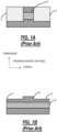
- planar optical waveguides used in Photonic Integrated Circuits are often broadly sorted into two categories by their strength of lateral guiding: strongly guided and weakly guided.
- the strength of lateral guiding determines how well the optical mode is confined to the central portion of the waveguide, and determines the minimum radius of curvature that a curved optical waveguide can achieve before the mode becomes unbound and radiates out of the waveguide.
- a waveguide 3 may consist of a core guiding region 5 with an optical index of refraction of Ng and a laterally adjacent cladding region 7 with optical index of refraction of Nc. Strong guiding refers to a large difference between Ng and Nc.
- weak guiding refers to designs where the core index Ng is only slightly higher than the cladding index Nc.
- An alternative weak guiding structure is shown in FIG.
- Such weakly guided waveguides 3 are also known as shallow ridge waveguides, and may have an index contrast Ng - Nc of ⁇ 0.05.
- MZMs Mach-Zehnder modulators
- Modulators of the sort described herein typically mix a Continuous Wave (CW) optical carrier input, having no data content, with a broadband electrical signal that carries data.
- the frequency of the CW carrier may be, for example, approximately 193 THz and is typically desired to be as narrowband as possible, for example 100 kHz line width.
- the bandwidth of the electrical data signal may span, for example, from 500 MHz to 10 GHz, or from 500 MHz to 70 GHz in modern high-capacity telecommunications systems. Depending on the modulation format being used, the bandwidth can provide a data rate of 10 Gbit/s to 400 Gbit/s or more.
- the data is transmitted as an optical carrier wave at the frequency of the original CW optical carrier input, with a modulation envelope determined by the electrical data signal.
- the modulators therefore, perform an up-conversion function from original Radio Frequency (RF) data baseband to optical frequencies, in order to enable transmission through optical fiber.
- RF Radio Frequency
- the modulators often further combine several RF data tributaries that are in an amplitude-modulated format into a more complex combined phase-and-amplitude-modulated format that may give advantages, for example, in the Signal to Noise Ratio (SNR) of the data at the receiving end of the fiber.
- SNR Signal to Noise Ratio
- the CW optical carrier input is critical to the function of such modulators.
- the CW optical carrier is provided by an external laser that is coupled through a short length of optical fiber to the modulator input if they are packaged separately, or through a microlens or optical guiding system if they are co-packaged.
- the light lost during the coupling and modulation processes is an important performance parameter. If too much of the CW optical carrier light is lost, the up-converted data signal emitted from the modulator will have low power, and is subject to a poor SNR at the receiver.
- One obvious solution is to use a high-power laser to compensate the losses.
- laser integration could also be combined with an integrated SOA to further boost the optical output power.
- Lasers and SOAs can be referred to generally as active or gain elements. Whether it is a laser or SOA, the state of the art in lateral optical guiding means is essentially similar. Often with such integration comes the need to integrate photonic components other than a modulator, laser, or SOA: detectors, optical monitors, phase tuning elements, variable optical attenuators, and so on.
- the extension of this invention to the integration of a gain element (laser or SOA) with photonic components other than a modulator is thus fundamentally important.
- Known shallow ridge, or stripe, lasers and SOAs have a configuration similar to FIG. 1B .
- they In addition to being weakly guided, they lack lateral current confinement capability, such that current spreads non-uniformly and inefficiently over a large area, thereby reducing gain.
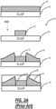
- BH laser and SOA structures come in numerous variants and represent the current industry standard, utilizing a more sophisticated arrangement of current-blocking layers to achieve better current confinement to the Multi-Quantum Well (MQW) core.
- MQW Multi-Quantum Well
- One shortcoming is the complex regrowth recipe that is difficult to monolithically integrate with a modulator in a manufacturable manner.
- BH lasers and SOAs with Al-containing cores are notorious for their questionable reliability.
- the BH structure 15 is manufactured by blanketing the N-InP wafer 10 with a first growth of MQW material 12. A selective etch is then performed to form a MQW ridge.
- a multi-layer stack 16 is selectively grown around the MQW ridge on the N-InP wafer 10, with sensitive critical dimensions. Finally, an overgrowth of P-type semiconductor 18 is blanketed over the MQW ridge and multi-layer stack 16. Although the current is much better confined, the waveguide is still weakly guided.
- the simplified BH structure 15b is manufactured by blanketing the N-InP wafer 10 with a first growth of MQW 12 and P-type semiconductor 18 material. A selective etch is performed to form an MQW ridge. Subsequently, a single, blanket layer of undoped InP 17 is grown over the structure 15. The undoped InP 17 is removed from the ridge top using a self-aligned etch technique. Like the more complex BH structure 15a ( FIG. 2A ), this simplified BH structure 15b ( FIG. 2B ) has good current confinement but is still weakly guided.
- Neither the shallow ridge structure ( FIG. 1B ) nor the BH structure ( FIG. 2B ) can be directly optically coupled to a modulator because the waveguides are incompatible. Some interconnection means is necessary to bridge the strongly guided and weakly guided waveguides, such as that provided in US 7,184,207 , for example.
- SAE Selective Area Epitaxy
- a patterned amorphous dielectric mask typically Silicon Dioxide (SiO 2 ) or Silicon Nitride (Si 3 N 4 )
- Semiconductor growth conditions are selected to ensure epitaxial growth on the exposed wafer, but not on the dielectric mask.
- SAE formed by covering parts of a semiconductor surface with a mask material on which growth does not occur.
- SAE is used to intentionally enhance the growth of epitaxial layers. The larger the area of the masked region the greater the increase in the rate of growth of the crystal adjacent to the mask. The degree of growth enhancement depends on many factors including, growth temperature, growth pressure, mask composition, mask area, and mask orientation.
- Suppressing unintentional enhancement by changing growth conditions has the disadvantage of also suppressing the intentional growth enhancement, which is often the purpose of pursuing SAE growth in the first place.
- the traditional use of straight-sided SAE masks leads to linear structures of enhanced growth material along the mask edge that is fragile and breaks off to form contamination of the device surface, which has an adverse effect on manufacturability and reliability.
- the present disclosure relates to systems and methods for a semiconductor device with Selective Area Epitaxy (SAE) growth utilizing a mask to suppress or enhance growth at the edges.
- SAE is a technique for crystal growth on semiconductor wafers. Areas of the wafer are covered or masked by thin layers of dielectric material (e.g., SiO 2 , Si 3 N 4 , etc.).
- dielectric material e.g., SiO 2 , Si 3 N 4 , etc.
- MOCVD Metal-Organic, Chemical-Vapor Deposition
- This disclosure provides a process for producing a semiconductor device containing areas of selective growth in an arbitrary orientation without unwanted growth enhancement and corresponding defects at the exterior edges of the masked areas. Specifically, the process includes variable profiles on the mask edges that can be used to suppress or enhance growth at the edges.
- the present disclosure provides a design whereby an optical amplifier is efficiently monolithically integrated with a deeply-etched ridge waveguide modulator, and, in particular, a multi-growth modulator formed on an InP wafer, such as that provided in US 9,182,546 , for example.
- the design enables the re-use of existing undoped overgrowth in the TWE modulator for the purpose of current blocking. Subsequent deep etching of the current-blocked buried ridge provides for independent control of the confinement factor and enables efficient coupling to a deeply-etched modulator.
- the present disclosure provides a means to re-use an overgrowth that already exists in the standard modulator process sequence, thereby reducing cost, complexity, and problems associated with many epitaxial growths, such as reliability issues.
- the present disclosure provides better current confinement, and therefore better electrical efficiency, than alternative shallow ridge solutions.
- the present disclosure decouples current confinement (provided by i-InP blocks described in greater detail herein below) from optical confinement (provided by etched areas described in greater detail herein below). Accordingly, the present disclosure provides an efficient alternative means to couple light from the modulator to the gain section without introducing an additional or new optical element into the design, such as that provided in US 7,184,207 , for example.
- the present disclosure provides a modulator with an optical amplifier, including: an N-type layer; a multi-quantum well material disposed on the N-type layer; a P-type layer disposed on the multi-quantum well material opposite the N-type layer; wherein a portion of the N-type layer, the multi-quantum well material, and a portion of the P-type layer collectively form a ridge structure; and a material that is not intentionally doped (commonly referred to as intrinsic, i-type) disposed on the N-type layer and about side portions of the ridge structure using selective area epitaxy.
- a modulator with an optical amplifier including: an N-type layer; a multi-quantum well material disposed on the N-type layer; a P-type layer disposed on the multi-quantum well material opposite the N-type layer; wherein a portion of the N-type layer, the multi-quantum well material, and a portion of the P-type layer collectively form a ridge structure; and a material that is not intentionally
- the common nomenclature for semiconductor that is not intentionally doped is i-type, it is understood by those skilled in the art that a low level of unintentional trace dopant contamination may exist in i-type material, sometimes up to concentrations of 1e16 atoms/cm 3 or more, although lower concentrations are typically desired.
- the i-type material is further deeply etched to form a strongly guided structure.
- the N-type layer includes N-InP.
- the P-type layer includes one of P-InGaAs and P-InP.
- the i-type material includes i-InP, but may alternatively be any type of suitable current-blocking material that impedes current flow, such as semi-insulating iron-doped InP.
- a width of the strongly guided structure is selected to couple efficiently to a strongly guided modulator waveguide.
- the present disclosure provides a design whereby an optical amplifier is efficiently monolithically integrated with a deeply-etched ridge waveguide modulator, and, in particular, a multi-growth modulator formed on an InP wafer, such as that provided in US 9,182,546 , for example.
- the design enables the re-use of existing undoped overgrowth in the TWE modulator for the purpose of current blocking. Subsequent deep etching of the current-blocked buried ridge provides for independent control of the confinement factor and enables efficient coupling to a deeply-etched modulator.
- the present disclosure provides a means to re-use an overgrowth that already exists in the standard modulator process sequence, thereby reducing cost, complexity, and problems associated with many epitaxial growths, such as reliability issues.
- the present disclosure provides better current confinement, and therefore better electrical efficiency, than alternative shallow ridge solutions.
- the present disclosure decouples current confinement (provided by i-InP blocks described in greater detail herein below) from optical confinement (provided by etched areas described in greater detail herein below). Accordingly, the present disclosure provides an efficient alternative means to couple light from the modulator to the gain section without introducing an additional or new optical element into the design, such as that provided in US 7,184,207 , for example.
- the present disclosure provides a modulator with an optical amplifier, including: an N-type layer; a multi-quantum well material disposed on the N-type layer; a P-type layer disposed on the multi-quantum well material opposite the N-type layer; wherein a portion of the N-type layer, the multi-quantum well material, and a portion of the P-type layer collectively form a ridge structure; and a material that is not intentionally doped (undoped, or i-type) disposed on the N-type layer and about side portions of the ridge structure using selective area epitaxy.
- the i-type material is further deeply etched to form a strongly guided structure.
- the N-type layer includes N-InP.
- the P-type layer includes one of P-InGaAs and P-InP.
- the i-type material includes i-InP, but may alternatively be any type of suitable current-blocking material that impedes current flow, such as semi-insulating iron-doped InP.
- a width of the strongly guided structure is selected to couple efficiently to a strongly guided modulator waveguide.
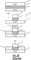
- FIG. 3 illustrates the fabrication of a conventional modulator structure 25, such as by the process provided in US 9,182,546 , for example.
- the modulator structure 25 is fabricated by blanketing the N-type wafer 10 with a first growth of MQW material 12 and a P-type layer 18.
- a selective etch of the P-type layer 18 is then performed, and a u-InP layer 20 is selectively grown in the etched area.
- the P-type layer 18 and MQW material 12 are then selectively etched, leaving a i-InP-capped ridge in the i-type ridge SOA embodiment and a P-type-capped ridge in a P-type ridge modulator embodiment.
- a selective i-type growth step is typically utilized. It is still desirable to monolithically integrate a SOA with a modulator and provide performance that approximates that of a BH structure 15 ( FIGS. 2A and 2B ), without the introduction of a critically-aligned growth step. It is also still desirable to, for the monolithically integrated SOA, create a BH-like structure that has a lateral optical mode that is compatible for optical coupling to a deeply etched modulator ridge.
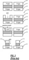
- the gain element structure 35 of the present disclosure is fabricated by blanketing an N-type layer 10 with a first growth of optical gain material 12 and a P-type layer 18.
- the P-type layer 18, optical gain material 12, and N-type layer 10 are then selectively etched, leaving a P-capped ridge that is covered with a mask 19.
- An i-type growth step is then utilized to fill the lateral areas of the ridge with i-InP material 20.
- the lateral i-InP material 20 provides superior current blocking, without the extra growth steps and critical alignments associated with BH fabrication
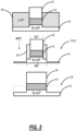
- FIG. 5 is a series of schematic diagrams illustrating the fabrication of another exemplary embodiment of the gain element structure 35 of the present disclosure, as well as the means for coupling of the associated SOA 37 and modulator 39.
- the i-InP material 20 and N-type material 10 are etched to form i-InP material walls on either side of the ridge, thereby providing strong guiding on either side of the ridge. Further, the deeply etched modulator waveguide can be widened to provide lateral optical matching.
- the bottom schematic represents the modulator waveguide that has been width-matched to the SOA input/output waveguide, shown in the middle schematic.
- W1 current confinement
- W2 optical mode overlap
- FIG. 6 is a schematic diagram illustrating the flaring of a waveguide SOA or modulator width to match an associated modulator SOA optical mode in accordance with the methods of the present disclosure.
- Any arbitrary combination of central width and exterior width, with tapers in between, is possible.
- only the central portion could be tapered, omitting the leading and trailing constant sections. This provides practical advantages for spatial hole burning by having high optical confinement at the beginning, and increasing injection, but lowering optical overlap at the end.
- FIG. 7 is another schematic diagram illustrating the flaring of the waveguide modulator width to match the SOA optical mode in accordance with the methods of the present disclosure.
- the SOA waveguide 37 is coupled to the modulator waveguide 39 via a tapering passive waveguide 38 or a tapering portion of the SOA waveguide 37 or modulator waveguide 39.
- i-InP layer 20 In the conventional modulator structure 25 of FIG. 3 , there is already a selective growth of i-InP layer 20, the thickness of which may be determined by the optimization of the modulator design. This same growth is used herein to provide better current blocking for a SOA. As shown in FIG 4 , the i-InP layer 20 from the conventional modulator may also be deposited on either side of the SOA ridge 19. The design requirements of the modulator 25, however, may not provide a thickness of i-InP layer 20 sufficient to match the height of the SOA ridge 19. To improve the manufacturability of subsequent processing steps, enhanced growth may be used to make a more planar top surface.
- width can be increased so as to improve the thermal impedance of the SOA.
- the deep etch ridge can be used.
- the present disclosure relates to systems and methods for a semiconductor device with Selective Area Epitaxy (SAE) growth utilizing a mask to suppress or enhance growth at the edges.
- SAE is a technique for crystal growth on semiconductor surfaces. Areas of the wafer are covered or masked by thin layers of dielectric material (e.g., SiO 2 , Si 3 N 4 , etc.).
- dielectric material e.g., SiO 2 , Si 3 N 4 , etc.
- MOCVD Metal-Organic Vapor-Phase Deposition
- This disclosure provides a process for producing a semiconductor device containing areas of selective growth in an arbitrary orientation without unwanted growth enhancement and corresponding defects at the exterior edges of the masked areas. Specifically, the process includes variable profiles on the mask edges that can be used to suppress or enhance growth at the edges.
- FIG. 8 illustrates a novel geometry 50 for the edge of a mask used to overgrow an epitaxial layer.
- a mask edge There is often an undesirable degree of enhanced crystal growth that occurs at the mask edge where the pattern is in the [011] or [0-11] directions, for example.
- the use of a non-linear geometry 50 for the mask edge suppresses this undesirable growth enhancement.
- the use of a zigzag pattern on the mask edge, rather than a straight edge, is a novel solution.
- Unintentional growth enhancement at a mask edge is an ongoing problem in selective area growth. Solutions to date have focused on altering the growth conditions for the epitaxial growth.
- Selective area epitaxy is a technique that is used in the production of many InP optical modulators.
- This technique and the use of mask patterns to reduce unintentional enhancement are related to multi-growth modulators on InP wafer as described in US 9,182,546 .
- Suppressing unintentional enhancement by changing growth conditions has the disadvantage of also suppressing the intentional growth enhancement, which is often the purpose of pursuing selective area growth in the first place.
- the conventional use of straight-sided selective area masks (SAMs) leads to linear structures of enhanced growth material along the mask edge that are fragile and break off to cause contamination of the device surface, which has an adverse effect on manufacturability and reliability.
- the use of a geometric solution 50 suppresses the intentional growth enhancement at the edge of the mask without compromising the intended growth enhancement.
- the effect of unintentional enhancement at a mask edge is anisotropic on the wafer surface.
- FIGS. 9A - 9D are block diagrams illustrating steps in an SAE growth process 95 on a wafer 100 to illustrate excess growth at edges of a mask 102.
- the wafer 100 can be a wafer including a wafer 104, a P island 106 of Indium Phosphide (InP), and a contact layer 108 including, e.g., Indium gallium arsenide (InGaAs).
- the mask 102 can include SiO 2 , and is deposited (applied) to the contact layer 108 at FIG. 9A .
- FIG. 9B a region is etched away through the mask 102, the P island 106, and the contact layer 108.
- SAE growth is performed in the etched region. Note, there is no SAE growth over the mask 100.
- FIG. 9D the mask 100 is removed.
- FIGS. 9C and 9D include excess growth 110 at the edge of the mask 100.
- FIG. 10 is a photograph of FIG. 9D in an actual wafer 100. Specifically, this illustrates the traditional use of straight-sided SAE masks 102 that leads to linear structures of enhanced growth 110 material along the mask edge that are fragile and break off to form contamination of the device surface, which has an adverse effect on manufacturability and reliability.
- FIG. 10 illustrates how, in the clean-up of the residual oxide, the excess growth 110 fractures along the edge of the P island 106 parallel to the major flat, but the edge parallel to the minor flat (perpendicular to the length of the waveguides) is clean.
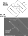
- FIG. 11A is a top view of a wafer 100 illustrating a region 140
- FIG. 11B is a photograph of the wafer 100 illustrating the region 140 and excess growth 110 that extends over the mask 102.
- the bare wafer is masked with oxide and has a thick overgrowth of InP in the region 140. This creates a "cap" of extra growth that overhangs the oxide. A subsequent etch is enough to remove the oxide under the cap, but it also tends to break off other material.
- FIGS. 12A and 12B are photographs illustrating a cross-section of the P island 106 in the direction of a waveguide ( FIG. 12A ) and perpendicular to the waveguide ( FIG. 12B ). It is noted in FIG. 12A the interface is well behaved in the direction of the waveguide. FIG. 12B , on the other hand, shows the excess growth broken off after the wet clean up. Prior to this, there is a large "mushroom cap" shape of InP. This feature leaves residual columns of material when subsequently etched.
- the present disclosure notes that specific, preferred angles for the mask 102, the adaptation of a shape and/or orientation of the mask 102, and/or zigzag edges of the mask 102 can lead to suppression (or enhancement) of growth at the edges of the mask 102.
- the mask 102 includes a specific geometry that suppresses or enhances the intentional growth enhancement at the edge of the mask 102 without compromising the intended growth enhancement, which is the purpose of SAE.
- the effect of unintentional enhancement at a mask edge is anisotropic on the wafer surface, i.e., it has a different value when measured in a different direction. Along one directional axis, the effect is strong, but along the perpendicular axis, it is weak. This is illustrated in FIGS. 12A and 12B .
- FIG. 13 is a diagram of an InP wafer 150 oriented in the (100) plane having a major flat 152 and a minor flat 154 perpendicular to the major flat 152, and a graph 160 of preferred directions of the wafer 100.
- a graph 162 illustrates an [011] axis 164 and a [011] axis 166 relative to the InP wafer 510 and the flats 152, 154.
- the terms axis and direction may be used interchangeably herein.
- the InP wafer 150 can be on the wafer 100. Note the locations of the major and minor flats follow one common convention but others may exist.
- growth enhancement passes through a null when an SAE mask 102 edge is aligned with one of the angles ("preferred angles") below relative to the [011] direction 164, collected into two series.
- Series 1 34 degrees 124 degrees 214 degrees 304 degrees
- Series 2 56 degrees 146 degrees 236 degrees 326 degrees
- each series contains four angular directions, with each direction separated by 90 degrees from the other three in the series.
- the graph 160 illustrates series 1, 2 in a graph format relative to the [011] direction 164. Note, while the angles in the series 1, 2 are specified relative to the [011] direction 164, those skilled in the art will appreciate these angles for the mask 102 edges could also be specified relative to any direction, including the [011] direction 166, as well as other crystallographic axes not illustrated herein. Also, note, those of ordinary skill in the art will recognize these angles are approximate values.
- FIG. 14 is a diagram of a rectangular mask 102A with an angled orientation according to the series 2 and a zigzag-shaped mask 102B with variable angles from both the series 1, 2.
- FIG. 15 is a diagram of the InP wafer 150 with an example mask 102A placed thereon.
- FIG. 16 is a diagram of the InP wafer 150 with an example mask 102B placed thereon.
- the InP wafer 150 can be on the order of centimeters in size (diameter), from the major flat 152 to the opposite side (top).
- the masks 102 are sized on the order of hundreds of microns in length and tens of microns in width, with the teeth of the zig-zag on the order of microns.
- the use of the mask 102 with the InP wafer 150 is utilized to form a semiconductor device with SAE, fabricated via a process of growing an epitaxial layer onto a semiconductor wafer 150.
- the semiconductor device includes 1) a first area covered by the mask 102 which inhibits crystal growth on the semiconductor wafer 150 surface, 2) a second area, complementary (adjacent) to the first area and not covered by the mask 102, which allows crystal growth on the semiconductor wafer 150, and 3) a perimeter of the mask 102 enclosing the first area and serving as a boundary between the first area and the second area, wherein most of the length of the perimeter is substantially aligned along a preferred crystal direction that provides reduced growth enhancement on the semiconductor wafer 150.
- the semiconductor wafer 150 can have portions where growth enhancement is desired and portions where growth enhancement is not desired, and this disclosure provides a degree of freedom to meet both needs. For example, enhanced growth can be desired for a spot-size converter, and minimal growth can be desired for a traveling-wave electrode.
- the mask 102A is in the shape of a quadrilateral, namely a polygon with four edges (or sides) and four vertices or corners. That is, the perimeter can be the quadrilateral. The key is that any of the four sides fall in line with the preferred angles.
- the mask 102B is in the shape of a series of zigzag patterns, namely the perimeter includes a series of small corners that fall in line with the preferred angles.
- the semiconductor wafer surface 150 is composed of a compound of group III and group V elements.
- the semiconductor wafer surface 150 is InP cut near the (100) orientation.
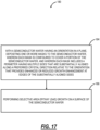
- FIG. 17 is a flowchart of a process 180 of growing an epitaxial layer onto a semiconductor wafer for a semiconductor device.
- the process 180 includes, with a semiconductor wafer having an orientation in a plane, depositing one or more masks to the semiconductor wafer, depositing one or more masks to the semiconductor wafer, wherein each mask is configured to cover a portion of the semiconductor wafer, and wherein each mask includes a perimeter having multiple sides that are substantially aligned along a preferred crystal direction relative to the orientation that provides enhanced or reduced growth enhancement at edges of the substantially aligned sides (step 184); and performing Selective Area Epitaxy (SAE) growth on a surface of the semiconductor wafer (step 186).
- SAE Selective Area Epitaxy
- the perimeter can have a shape of a quadrilateral or a series of zigzag patterns.
- the semiconductor wafer can include a compound of group III and group V elements.
- the semiconductor wafer can be Indium Phosphide (InP), and the plane can be near a (100) orientation.
- the preferred crystal direction can be one or more of angles having approximate degrees of 34, 124, 214, 304, 56, 146, 236, and 326, relative to a [011] direction of the semiconductor wafer.
- a mask is for a spot size converter, and the preferred crystal direction is selected to provide the maximum growth enhancement.
- a mask is for a traveling-wave electrode, and the preferred crystal direction is selected to provide the reduced growth enhancement.
- a semiconductor device can be formed by the process 180.
- a semiconductor device for fabrication via a process of growing an epitaxial layer onto a semiconductor wafer via Selective Area Epitaxy (SAE), includes a first area covered by a mask which inhibits crystal growth on a surface of the first area; a second area, adjacent to the first area and not covered by a mask, which allows crystal growth on a surface of the second area; and a perimeter of the mask serving as a boundary between the first area and the second area, wherein multiple sides of the perimeter are substantially aligned along a preferred crystal direction relative to an orientation of the semiconductor wafer, to minimize or maximize growth enhancement at edges of the substantially aligned sides.
- SAE Selective Area Epitaxy
- FIG. 18 is a photograph of a circular mask within a high-resolution Field of View (FOV), to illustrate how the preferred angles were determined.
- the circular mask represents all possible angle values (0 to 360 degrees) relative to the [011] direction 164.
- the preferred crystal direction is one or more of the following angles relative to the [011] direction of the InP wafer 150, in approximate degrees: 34, 124, 214, 304, 56, 146, 236, 326.
- Those skilled in the art will recognize this same approach, namely using a circular mask to experimentally determine growth properties at different angles, could be used on other types of wafers 100, with other crystallographic axes, etc. to determine preferred mask 102 angles.
Landscapes
- Physics & Mathematics (AREA)
- General Physics & Mathematics (AREA)
- Optics & Photonics (AREA)
- Electromagnetism (AREA)
- Condensed Matter Physics & Semiconductors (AREA)
- Engineering & Computer Science (AREA)
- Geometry (AREA)
- Microelectronics & Electronic Packaging (AREA)
- Nonlinear Science (AREA)
- Power Engineering (AREA)
- Optical Integrated Circuits (AREA)
- Optical Modulation, Optical Deflection, Nonlinear Optics, Optical Demodulation, Optical Logic Elements (AREA)
- Recrystallisation Techniques (AREA)
Applications Claiming Priority (3)
| Application Number | Priority Date | Filing Date | Title |
|---|---|---|---|
| US16/423,846 US10852478B1 (en) | 2019-05-28 | 2019-05-28 | Monolithically integrated gain element |
| EP20747162.4A EP3963677B1 (de) | 2019-05-28 | 2020-05-28 | Monolithisch integriertes verstärkungselement |
| PCT/US2020/034888 WO2020243279A1 (en) | 2019-05-28 | 2020-05-28 | Monolithically integrated gain element |
Related Parent Applications (1)
| Application Number | Title | Priority Date | Filing Date |
|---|---|---|---|
| EP20747162.4A Division EP3963677B1 (de) | 2019-05-28 | 2020-05-28 | Monolithisch integriertes verstärkungselement |
Publications (2)
| Publication Number | Publication Date |
|---|---|
| EP4451489A2 true EP4451489A2 (de) | 2024-10-23 |
| EP4451489A3 EP4451489A3 (de) | 2025-01-29 |
Family
ID=73551246
Family Applications (2)
| Application Number | Title | Priority Date | Filing Date |
|---|---|---|---|
| EP24199592.7A Pending EP4451489A3 (de) | 2019-05-28 | 2020-05-28 | Monolithisch integriertes verstärkungselement |
| EP20747162.4A Active EP3963677B1 (de) | 2019-05-28 | 2020-05-28 | Monolithisch integriertes verstärkungselement |
Family Applications After (1)
| Application Number | Title | Priority Date | Filing Date |
|---|---|---|---|
| EP20747162.4A Active EP3963677B1 (de) | 2019-05-28 | 2020-05-28 | Monolithisch integriertes verstärkungselement |
Country Status (2)
| Country | Link |
|---|---|
| US (1) | US10852478B1 (de) |
| EP (2) | EP4451489A3 (de) |
Families Citing this family (4)
| Publication number | Priority date | Publication date | Assignee | Title |
|---|---|---|---|---|
| CN110249245B (zh) * | 2017-02-07 | 2021-02-19 | 古河电气工业株式会社 | 光波导构造 |
| US11869991B2 (en) * | 2020-09-18 | 2024-01-09 | Taiwan Semiconductor Manufacturing Company Limited | Semiconductor device and method of making |
| GB202207452D0 (en) * | 2022-05-20 | 2022-07-06 | Sivers Photonics Ltd | Ridge waveguide photonic devices with improved lateal current confinement |
| EP4572039A1 (de) * | 2023-12-14 | 2025-06-18 | Nokia Solutions and Networks Oy | Semi-isolierender bündelquerschnitt umwandler mit grosser brechzahl zur optischen kopplung von iii-v an silizium-heterointegrierte schaltungen |
Citations (2)
| Publication number | Priority date | Publication date | Assignee | Title |
|---|---|---|---|---|
| US7184207B1 (en) | 2005-09-27 | 2007-02-27 | Bookham Technology Plc | Semiconductor optical device |
| US9182546B2 (en) | 2008-12-16 | 2015-11-10 | Fraunhofer-Gesellschaft Zur Forderung Der Angewandten Forschung E.V. | Monolithic optoelectronic TWE-component structure for high frequencies and low optical insertion loss |
Family Cites Families (44)
| Publication number | Priority date | Publication date | Assignee | Title |
|---|---|---|---|---|
| US4727047A (en) * | 1980-04-10 | 1988-02-23 | Massachusetts Institute Of Technology | Method of producing sheets of crystalline material |
| DE3886337D1 (de) * | 1987-10-15 | 1994-01-27 | Toshiba Kawasaki Kk | Halbleiteranordnungen und Herstellungsverfahren. |
| US4928285A (en) * | 1988-02-23 | 1990-05-22 | Kabushiki Kaisha Toshiba | Impurity-doped semiconductor laser device for single wavelength oscillation |
| US5799119A (en) | 1996-07-03 | 1998-08-25 | Northern Telecom Limited | Coupling of strongly and weakly guiding waveguides for compact integrated mach zehnder modulators |
| GB2326020B (en) * | 1997-06-06 | 2002-05-15 | Ericsson Telefon Ab L M | Waveguide |
| EP0905546A3 (de) | 1997-09-26 | 2002-06-19 | Nippon Telegraph and Telephone Corporation | Gestapelter thermooptischer Schalter, Schaltmatrix und Ein-/Ausfügemultiplexer mit dem gestapelten thermooptischen Schalter |
| US6058226A (en) | 1997-10-24 | 2000-05-02 | D-Star Technologies Llc | Optical fiber sensors, tunable filters and modulators using long-period gratings |
| JP2000066156A (ja) | 1998-08-25 | 2000-03-03 | Mitsubishi Electric Corp | マッハツェンダ型光変調器 |
| JP2000101186A (ja) | 1998-09-25 | 2000-04-07 | Nec Corp | 半導体光素子およびその製造方法 |
| JP3784585B2 (ja) | 1999-08-26 | 2006-06-14 | 富士通株式会社 | 光ファイバ伝送のための方法、光デバイス及びシステム |
| KR100406865B1 (ko) | 1999-11-04 | 2003-11-21 | 삼성전자주식회사 | 선택 영역 성장법을 이용한 2중 코아 스폿 사이즈 변환기및 그 제조방법 |
| JP2001264561A (ja) | 2000-03-15 | 2001-09-26 | Fuji Xerox Co Ltd | 光導波路素子、光導波路素子の製造方法、光偏向素子、及び光スイッチ素子 |
| JP2002107681A (ja) | 2000-09-29 | 2002-04-10 | Fujitsu Quantum Devices Ltd | 光半導体装置 |
| US6654534B1 (en) | 2000-11-13 | 2003-11-25 | Bookham Technology, Plc | Electrode, termination for reduced local heating in an optical device |
| KR20020077567A (ko) * | 2001-04-02 | 2002-10-12 | 한국전자통신연구원 | 광모드 크기 변환기가 결합된 레이저 및 그 제조 방법 |
| JP2003131055A (ja) | 2001-10-25 | 2003-05-08 | Fujitsu Ltd | 光導波路及びその製造方法 |
| KR100413527B1 (ko) | 2002-01-29 | 2004-01-03 | 한국전자통신연구원 | 단일 집적 반도체 광소자 제작방법 |
| US20080008416A1 (en) | 2002-02-12 | 2008-01-10 | Bookham Technology, Plc | Opto-electronic device |
| US6717708B2 (en) | 2002-04-05 | 2004-04-06 | Bookham Technology, Plc | Re-circulating optical pulse generator |
| US7035305B2 (en) | 2002-05-10 | 2006-04-25 | Bookham Technology, Plc | Monolithically integrated high power laser optical device |
| US6650458B1 (en) | 2002-09-26 | 2003-11-18 | Bookham Technology Plc | Electro-optic modulator with continuously adjustable chirp |
| US20050169342A1 (en) | 2003-10-30 | 2005-08-04 | Bookham Technology Plc | DFB grating with dopant induced refractive index change |
| US20050135733A1 (en) | 2003-12-19 | 2005-06-23 | Benoit Reid | Integrated optical loop mirror |
| US20050201437A1 (en) | 2004-03-15 | 2005-09-15 | Benoit Reid | Semiconductor laser |
| GB0424253D0 (en) | 2004-05-20 | 2004-12-01 | Bookham Technology Plc | Laterally implanted electro-absorption modulated laser |
| KR100651477B1 (ko) * | 2005-01-19 | 2006-11-29 | 삼성전자주식회사 | 반도체 레이저와 반도체 레이저의 제작 방법 |
| JP4584079B2 (ja) * | 2005-08-31 | 2010-11-17 | 富士通株式会社 | 半導体光増幅器および光集積回路 |
| WO2007036702A1 (en) | 2005-09-27 | 2007-04-05 | Bookham Technology Plc | Multi-mode interference optical devices |
| KR100842277B1 (ko) * | 2006-12-07 | 2008-06-30 | 한국전자통신연구원 | 반사형 반도체 광증폭기 및 수퍼 루미네센스 다이오드 |
| JP4794505B2 (ja) * | 2007-06-15 | 2011-10-19 | 富士通株式会社 | 半導体光増幅装置、半導体光増幅システム及び半導体光集積素子 |
| JP5374894B2 (ja) * | 2008-03-18 | 2013-12-25 | 富士通株式会社 | 半導体光増幅器及びその製造方法並びに半導体光集積素子 |
| JP2010232424A (ja) * | 2009-03-27 | 2010-10-14 | Fujitsu Ltd | 半導体光増幅装置及び光モジュール |
| KR20110064148A (ko) * | 2009-12-07 | 2011-06-15 | 한국전자통신연구원 | 광 소자 모듈 |
| US8280201B2 (en) | 2009-12-08 | 2012-10-02 | COGO Oprtonics, Inc. | Traveling wave Mach-Zehnder optical device |
| JP5573386B2 (ja) | 2010-06-10 | 2014-08-20 | 三菱電機株式会社 | 半導体光集積素子及びその製造方法 |
| KR101754280B1 (ko) * | 2011-05-04 | 2017-07-07 | 한국전자통신연구원 | 반도체 광 소자 및 그 제조 방법 |
| US8917958B2 (en) | 2011-12-22 | 2014-12-23 | Teraxion Inc. | Electrical waveguide transmission device for use with a mach-zehnder optical modulator |
| US9069223B2 (en) | 2012-02-15 | 2015-06-30 | Teraxion Inc. | Mach-Zehnder optical modulator using a balanced coplanar stripline with lateral ground planes |
| JP2014041889A (ja) | 2012-08-22 | 2014-03-06 | Mitsubishi Electric Corp | 光半導体装置 |
| US8903202B1 (en) | 2012-11-09 | 2014-12-02 | Teraxion Inc. | Mach-Zehnder optical modulator having a travelling wave electrode with a distributed ground bridging structure |
| US9008469B2 (en) | 2012-11-09 | 2015-04-14 | Teraxion Inc. | Mach-zehnder optical modulator having an asymmetrically-loaded traveling wave electrode |
| US9244327B2 (en) | 2013-04-26 | 2016-01-26 | Teraxion Inc. | Mach-Zehnder modulator with backplane voltage equalization |
| US9482925B2 (en) | 2013-08-02 | 2016-11-01 | Ciena Corporation | Mach-Zehnder optical modulator with embedded active elements |
| US9804425B1 (en) | 2016-10-20 | 2017-10-31 | Ciena Corporation | Optical system with band gap tuning |
-
2019
- 2019-05-28 US US16/423,846 patent/US10852478B1/en active Active
-
2020
- 2020-05-28 EP EP24199592.7A patent/EP4451489A3/de active Pending
- 2020-05-28 EP EP20747162.4A patent/EP3963677B1/de active Active
Patent Citations (2)
| Publication number | Priority date | Publication date | Assignee | Title |
|---|---|---|---|---|
| US7184207B1 (en) | 2005-09-27 | 2007-02-27 | Bookham Technology Plc | Semiconductor optical device |
| US9182546B2 (en) | 2008-12-16 | 2015-11-10 | Fraunhofer-Gesellschaft Zur Forderung Der Angewandten Forschung E.V. | Monolithic optoelectronic TWE-component structure for high frequencies and low optical insertion loss |
Also Published As
| Publication number | Publication date |
|---|---|
| US20200379174A1 (en) | 2020-12-03 |
| EP3963677A1 (de) | 2022-03-09 |
| EP4451489A3 (de) | 2025-01-29 |
| EP3963677B1 (de) | 2024-09-11 |
| US10852478B1 (en) | 2020-12-01 |
Similar Documents
| Publication | Publication Date | Title |
|---|---|---|
| EP3963677B1 (de) | Monolithisch integriertes verstärkungselement | |
| US20260039091A1 (en) | Semiconductor Device With Selective Area Epitaxy Growth Utilizing a Mask to Suppress or Enhance Growth at the Edges | |
| US9229293B2 (en) | Semiconductor optical device and method for manufacturing semiconductor optical device | |
| US6162655A (en) | Method of fabricating an expanded beam optical waveguide device | |
| US7454111B2 (en) | Optical device of waveguide type and its production method | |
| CA2292907C (en) | Waveguide | |
| US20080159347A1 (en) | Method and apparatus for a low parasitic capacitance butt-joined passive waveguide connected to an active structure | |
| US7184640B2 (en) | Buried heterostructure device fabricated by single step MOCVD | |
| US10684414B1 (en) | Interconnect between different multi-quantum well waveguides in a semiconductor photonic integrated circuit | |
| KR0155509B1 (ko) | 반도체 광집적소자의 제조방법 | |
| KR100369329B1 (ko) | 무결함, 무반사의 스폿사이즈 변환기를 구비한 광소자의제조 방법 | |
| US20150185582A1 (en) | Mask design and method of fabricating a mode converter optical semiconductor device | |
| CN117410825A (zh) | 一种基于bh结构的eml激光器芯片及其制备方法 | |
| US6503768B2 (en) | Method for monolithic integration of multiple devices on an optoelectronic substrate | |
| EP1193771A2 (de) | Herstellungsverfahren eines Halbleiter-Bauelements | |
| JP2005520328A (ja) | 光通信デバイスを製造する方法および光通信デバイス | |
| Shima et al. | Buried convex waveguide structure (GaAl) As injection lasers | |
| WO2026034327A1 (ja) | 光回路 | |
| CN121149789A (zh) | 一种异质集成硅基激光器的制备方法及相关产品 | |
| CN119834058A (zh) | 选择性生长的高速电吸收调制激光器芯片及其制备方法 | |
| KR100248430B1 (ko) | 광도파로 집적 반도체 레이저 구조 및 그 제조방법 | |
| Alexandre et al. | Butt-coupled waveguide-modulators by low temperature embedded CBE regrowth for high speed modulation (42 GHz) or large extinction ratio (> 50 db) | |
| KR20000055917A (ko) | 반도체 레이저 다이오드 및 그 제조방법 |
Legal Events
| Date | Code | Title | Description |
|---|---|---|---|
| PUAI | Public reference made under article 153(3) epc to a published international application that has entered the european phase |
Free format text: ORIGINAL CODE: 0009012 |
|
| STAA | Information on the status of an ep patent application or granted ep patent |
Free format text: STATUS: THE APPLICATION HAS BEEN PUBLISHED |
|
| AC | Divisional application: reference to earlier application |
Ref document number: 3963677 Country of ref document: EP Kind code of ref document: P |
|
| AK | Designated contracting states |
Kind code of ref document: A2 Designated state(s): AL AT BE BG CH CY CZ DE DK EE ES FI FR GB GR HR HU IE IS IT LI LT LU LV MC MK MT NL NO PL PT RO RS SE SI SK SM TR |
|
| REG | Reference to a national code |
Ref country code: DE Ref legal event code: R079 Free format text: PREVIOUS MAIN CLASS: H01S0005220000 Ipc: H01L0021200000 |
|
| PUAL | Search report despatched |
Free format text: ORIGINAL CODE: 0009013 |
|
| AK | Designated contracting states |
Kind code of ref document: A3 Designated state(s): AL AT BE BG CH CY CZ DE DK EE ES FI FR GB GR HR HU IE IS IT LI LT LU LV MC MK MT NL NO PL PT RO RS SE SI SK SM TR |
|
| RIC1 | Information provided on ipc code assigned before grant |
Ipc: G02B 6/122 20060101ALN20241223BHEP Ipc: G02B 6/12 20060101ALN20241223BHEP Ipc: H01S 5/343 20060101ALN20241223BHEP Ipc: H01S 5/227 20060101ALN20241223BHEP Ipc: H01S 5/10 20210101ALN20241223BHEP Ipc: G02F 1/025 20060101ALI20241223BHEP Ipc: H01S 5/50 20060101ALI20241223BHEP Ipc: H01S 5/20 20060101ALI20241223BHEP Ipc: H01S 5/026 20060101ALI20241223BHEP Ipc: H01L 21/3205 20060101ALI20241223BHEP Ipc: H01S 5/22 20060101ALI20241223BHEP Ipc: H01L 21/20 20060101AFI20241223BHEP |
|
| P01 | Opt-out of the competence of the unified patent court (upc) registered |
Free format text: CASE NUMBER: APP_4997/2025 Effective date: 20250130 |
|
| STAA | Information on the status of an ep patent application or granted ep patent |
Free format text: STATUS: REQUEST FOR EXAMINATION WAS MADE |
|
| 17P | Request for examination filed |
Effective date: 20250522 |