EP4572039A1 - Semi-isolierender bündelquerschnitt umwandler mit grosser brechzahl zur optischen kopplung von iii-v an silizium-heterointegrierte schaltungen - Google Patents
Semi-isolierender bündelquerschnitt umwandler mit grosser brechzahl zur optischen kopplung von iii-v an silizium-heterointegrierte schaltungen Download PDFInfo
- Publication number
- EP4572039A1 EP4572039A1 EP23307208.1A EP23307208A EP4572039A1 EP 4572039 A1 EP4572039 A1 EP 4572039A1 EP 23307208 A EP23307208 A EP 23307208A EP 4572039 A1 EP4572039 A1 EP 4572039A1
- Authority
- EP
- European Patent Office
- Prior art keywords
- cladding
- photonic device
- inferior
- iii
- regrown layer
- Prior art date
- Legal status (The legal status is an assumption and is not a legal conclusion. Google has not performed a legal analysis and makes no representation as to the accuracy of the status listed.)
- Pending
Links
Images

Classifications
-
- H—ELECTRICITY
- H01—ELECTRIC ELEMENTS
- H01S—DEVICES USING THE PROCESS OF LIGHT AMPLIFICATION BY STIMULATED EMISSION OF RADIATION [LASER] TO AMPLIFY OR GENERATE LIGHT; DEVICES USING STIMULATED EMISSION OF ELECTROMAGNETIC RADIATION IN WAVE RANGES OTHER THAN OPTICAL
- H01S5/00—Semiconductor lasers
- H01S5/02—Structural details or components not essential to laser action
- H01S5/0206—Substrates, e.g. growth, shape, material, removal or bonding
- H01S5/021—Silicon based substrates
-
- H—ELECTRICITY
- H01—ELECTRIC ELEMENTS
- H01S—DEVICES USING THE PROCESS OF LIGHT AMPLIFICATION BY STIMULATED EMISSION OF RADIATION [LASER] TO AMPLIFY OR GENERATE LIGHT; DEVICES USING STIMULATED EMISSION OF ELECTROMAGNETIC RADIATION IN WAVE RANGES OTHER THAN OPTICAL
- H01S5/00—Semiconductor lasers
- H01S5/02—Structural details or components not essential to laser action
- H01S5/026—Monolithically integrated components, e.g. waveguides, monitoring photo-detectors, drivers
-
- H—ELECTRICITY
- H01—ELECTRIC ELEMENTS
- H01S—DEVICES USING THE PROCESS OF LIGHT AMPLIFICATION BY STIMULATED EMISSION OF RADIATION [LASER] TO AMPLIFY OR GENERATE LIGHT; DEVICES USING STIMULATED EMISSION OF ELECTROMAGNETIC RADIATION IN WAVE RANGES OTHER THAN OPTICAL
- H01S5/00—Semiconductor lasers
- H01S5/10—Construction or shape of the optical resonator, e.g. extended or external cavity, coupled cavities, bent-guide, varying width, thickness or composition of the active region
- H01S5/1003—Waveguide having a modified shape along the axis, e.g. branched, curved, tapered, voids
- H01S5/1014—Tapered waveguide, e.g. spotsize converter
-
- H—ELECTRICITY
- H01—ELECTRIC ELEMENTS
- H01S—DEVICES USING THE PROCESS OF LIGHT AMPLIFICATION BY STIMULATED EMISSION OF RADIATION [LASER] TO AMPLIFY OR GENERATE LIGHT; DEVICES USING STIMULATED EMISSION OF ELECTROMAGNETIC RADIATION IN WAVE RANGES OTHER THAN OPTICAL
- H01S5/00—Semiconductor lasers
- H01S5/20—Structure or shape of the semiconductor body to guide the optical wave ; Confining structures perpendicular to the optical axis, e.g. index or gain guiding, stripe geometry, broad area lasers, gain tailoring, transverse or lateral reflectors, special cladding structures, MQW barrier reflection layers
- H01S5/22—Structure or shape of the semiconductor body to guide the optical wave ; Confining structures perpendicular to the optical axis, e.g. index or gain guiding, stripe geometry, broad area lasers, gain tailoring, transverse or lateral reflectors, special cladding structures, MQW barrier reflection layers having a ridge or stripe structure
- H01S5/227—Buried mesa structure ; Striped active layer
-
- H—ELECTRICITY
- H01—ELECTRIC ELEMENTS
- H01S—DEVICES USING THE PROCESS OF LIGHT AMPLIFICATION BY STIMULATED EMISSION OF RADIATION [LASER] TO AMPLIFY OR GENERATE LIGHT; DEVICES USING STIMULATED EMISSION OF ELECTROMAGNETIC RADIATION IN WAVE RANGES OTHER THAN OPTICAL
- H01S5/00—Semiconductor lasers
- H01S5/02—Structural details or components not essential to laser action
- H01S5/022—Mountings; Housings
- H01S5/0233—Mounting configuration of laser chips
- H01S5/02345—Wire-bonding
-
- H—ELECTRICITY
- H01—ELECTRIC ELEMENTS
- H01S—DEVICES USING THE PROCESS OF LIGHT AMPLIFICATION BY STIMULATED EMISSION OF RADIATION [LASER] TO AMPLIFY OR GENERATE LIGHT; DEVICES USING STIMULATED EMISSION OF ELECTROMAGNETIC RADIATION IN WAVE RANGES OTHER THAN OPTICAL
- H01S5/00—Semiconductor lasers
- H01S5/04—Processes or apparatus for excitation, e.g. pumping, e.g. by electron beams
- H01S5/042—Electrical excitation ; Circuits therefor
- H01S5/0425—Electrodes, e.g. characterised by the structure
- H01S5/04256—Electrodes, e.g. characterised by the structure characterised by the configuration
- H01S5/04257—Electrodes, e.g. characterised by the structure characterised by the configuration having positive and negative electrodes on the same side of the substrate
-
- H—ELECTRICITY
- H01—ELECTRIC ELEMENTS
- H01S—DEVICES USING THE PROCESS OF LIGHT AMPLIFICATION BY STIMULATED EMISSION OF RADIATION [LASER] TO AMPLIFY OR GENERATE LIGHT; DEVICES USING STIMULATED EMISSION OF ELECTROMAGNETIC RADIATION IN WAVE RANGES OTHER THAN OPTICAL
- H01S5/00—Semiconductor lasers
- H01S5/10—Construction or shape of the optical resonator, e.g. extended or external cavity, coupled cavities, bent-guide, varying width, thickness or composition of the active region
- H01S5/1028—Coupling to elements in the cavity, e.g. coupling to waveguides adjacent the active region, e.g. forward coupled [DFC] structures
- H01S5/1032—Coupling to elements comprising an optical axis that is not aligned with the optical axis of the active region
-
- H—ELECTRICITY
- H01—ELECTRIC ELEMENTS
- H01S—DEVICES USING THE PROCESS OF LIGHT AMPLIFICATION BY STIMULATED EMISSION OF RADIATION [LASER] TO AMPLIFY OR GENERATE LIGHT; DEVICES USING STIMULATED EMISSION OF ELECTROMAGNETIC RADIATION IN WAVE RANGES OTHER THAN OPTICAL
- H01S5/00—Semiconductor lasers
- H01S5/20—Structure or shape of the semiconductor body to guide the optical wave ; Confining structures perpendicular to the optical axis, e.g. index or gain guiding, stripe geometry, broad area lasers, gain tailoring, transverse or lateral reflectors, special cladding structures, MQW barrier reflection layers
- H01S5/22—Structure or shape of the semiconductor body to guide the optical wave ; Confining structures perpendicular to the optical axis, e.g. index or gain guiding, stripe geometry, broad area lasers, gain tailoring, transverse or lateral reflectors, special cladding structures, MQW barrier reflection layers having a ridge or stripe structure
- H01S5/2205—Structure or shape of the semiconductor body to guide the optical wave ; Confining structures perpendicular to the optical axis, e.g. index or gain guiding, stripe geometry, broad area lasers, gain tailoring, transverse or lateral reflectors, special cladding structures, MQW barrier reflection layers having a ridge or stripe structure comprising special burying or current confinement layers
- H01S5/2222—Structure or shape of the semiconductor body to guide the optical wave ; Confining structures perpendicular to the optical axis, e.g. index or gain guiding, stripe geometry, broad area lasers, gain tailoring, transverse or lateral reflectors, special cladding structures, MQW barrier reflection layers having a ridge or stripe structure comprising special burying or current confinement layers having special electric properties
- H01S5/2224—Structure or shape of the semiconductor body to guide the optical wave ; Confining structures perpendicular to the optical axis, e.g. index or gain guiding, stripe geometry, broad area lasers, gain tailoring, transverse or lateral reflectors, special cladding structures, MQW barrier reflection layers having a ridge or stripe structure comprising special burying or current confinement layers having special electric properties semi-insulating semiconductors
-
- H—ELECTRICITY
- H01—ELECTRIC ELEMENTS
- H01S—DEVICES USING THE PROCESS OF LIGHT AMPLIFICATION BY STIMULATED EMISSION OF RADIATION [LASER] TO AMPLIFY OR GENERATE LIGHT; DEVICES USING STIMULATED EMISSION OF ELECTROMAGNETIC RADIATION IN WAVE RANGES OTHER THAN OPTICAL
- H01S5/00—Semiconductor lasers
- H01S5/30—Structure or shape of the active region; Materials used for the active region
- H01S5/32—Structure or shape of the active region; Materials used for the active region comprising PN junctions, e.g. hetero- or double- heterostructures
- H01S5/323—Structure or shape of the active region; Materials used for the active region comprising PN junctions, e.g. hetero- or double- heterostructures in AIIIBV compounds, e.g. AlGaAs-laser, InP-based laser
- H01S5/3235—Structure or shape of the active region; Materials used for the active region comprising PN junctions, e.g. hetero- or double- heterostructures in AIIIBV compounds, e.g. AlGaAs-laser, InP-based laser emitting light at a wavelength longer than 1000 nm, e.g. InP-based 1300 nm and 1500 nm lasers
Definitions
- Various example embodiments relate to optical components, notably to photonic devices. More particularly, a photonic device comprising a III-V structure with a regrown layer and being suitable for edge coupling is disclosed.
- Semiconductor based optical components are used in optical networks to emit, modulate and detect light, and to perform some optical processing like amplification, multiplexing, demultiplexing, and demodulation.
- Optical coupling of these components to optical fibers is a crucial parameter to limit insertion losses of optical components.
- typical optical components have submicron mode size whereas optical fibers typically have a beam diameter of around 10 ⁇ m or 3-5 ⁇ m for lensed fibers, thus generating coupling losses between the optical component and the optical fiber.
- the photonic device with a longitudinal direction of light propagation comprises:
- the photonic device may further comprise an interface deposited on the substrate and separating the III-V structure from the substrate, the interface having a high refractive index contrast with respect to the III-V materials.
- the transition portion may comprise an extremal end opposite the main portion along the longitudinal direction in which the regrown layer has a constant section.
- the active core and the superior cladding may not extend in a distal part of the extremal end.
- the transition portion may comprise a proximal end next to the main portion in which the width of the regrown layer decreases gradually.
- the inferior cladding may be narrower at least in part of the transition portion than in the main portion.
- the inferior cladding may have the same width as the regrown layer in the tip of the extremal end.
- the inferior cladding and the regrown layer may form an assembly with a rectangular cross-section in the tip of the extremal end.
- the transition portion may comprise an intermediary part between the proximal end and the tip of the extremal end in which the width of the inferior cladding decreases gradually.
- the inferior cladding may be made of N type materials and the superior cladding is made of P type materials.
- the interface may extend vertically on either side of the regrown layer in the transition portion.
- the semi-insulating material of the regrown layer may be Indium Phosphide.
- the interface portion may be made of SiO2.
- the photonic device may further comprise at least two electrical connection zones among which a first electrical connection in contact with the inferior cladding and a second electrical connection in contact with the superior cladding.
- the regrown layer may form a two stages III-V passive waveguide comprising:
- Another embodiment relates to an optical device comprising a photonic device as described above, wherein the optical device is one of a laser, a resonator, an interferometer, a light filter and a light routing device.
- the method of fabrication of a photonic device with a longitudinal direction of light propagation comprises the following steps:
- the vertical, longitudinal, and transverse orientations according to the reference frame V, L, T shown in the figures, whose longitudinal L and transverse T axes extend in a horizontal plane, will be adopted as nonlimiting and without restrictive reference to terrestrial gravity.
- the vertical axis V is oriented from bottom to top.
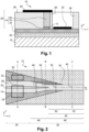
- Figure 1 illustrates a photonic device 10 according to a first embodiment.
- the photonic device 10 allows to obtain highly efficient edge coupling to external components as optical fibers, or other passive components.
- the photonic device 10 comprises a III-V on Silicon Hetero-integrated photonic device.
- the Hetero-integrated photonic device comprises a substrate, a PIN junction made of III-V materials and a III-V regrown layer. Integration of III-V components on silicon may be used to generate optical gain on low-cost silicon platform.
- the photonic device 10 comprises: a substrate 12, an PIN junction 14, a regrown layer 26 and at least two electrical connection zones 22, 24.
- the PIN junction 14 is adapted for emitting light O in the case of an emitter or for absorbing light O in the case of a receiver.
- the PIN junction comprises an active core 16, an inferior cladding 18 and a superior cladding 20.
- the active core 16 is placed in between or surrounded by an inferior cladding 18 and a superior cladding 20 among which one is made of N type and the other of P type materials.
- Each cladding is a semiconductor layer stack.
- the at least two electrical connection zones 22, 24 include a first electrical connection 22 in contact with the inferior cladding 18 and a second electrical connection 24 in contact with the superior cladding 20.
- the substrate 12 can be made of silicon (Si).
- the substrate 12 can also be made of glass or silicon carbide (SiC).
- the inferior cladding is made of N type materials (i.e. N doped materials) and the superior cladding 20 is made of P type materials (i.e. N doped materials).
- the inferior cladding 18 can be made of P type materials and the superior cladding 20 can be made of N type materials.
- a semi-insulating material is regrown around the PIN junction 14 to generate a regrown layer 26.
- the regrown layer 26 allows to optimize thermal dissipation.
- the regrowth of semi-insulating material like indium phosphide (InP) on a silicon substrate is a complex technique due to lattice and thermal expansion coefficient mismatch. This is the reason why, traditionally, a simpler technology is used that results in a photonic device comprising a single epitaxial III-V stack.
- Regrowing semi-insulating material on a III-V on Silicon Hetero-integrated photonic device is a technique that has been recently developed and described in the patent published under the reference EP2809540 . This technique considerably improves performance in terms of heat dissipation of the PIN junction 14.
- the regrowth of a semi-insulating material on both sides of the active core 16 and of the superior cladding 20 leads to a buried structure, in which the optical waveguide comprising the PIN junction 14 is buried into regrown semi-insulating material. After regrowth, the regrown layer 26 forms lateral edges of the optical waveguide, while the inferior cladding forms the bottom of the optical waveguide and the superior cladding forms the top of the optical waveguide.
- the photonic device 10 comprises a regrown layer 26 made of semi-insulating material on top of at least part of the inferior cladding 18 and extending vertically on either side of the active core 16 and of the superior cladding 20.
- the photonic device 10 comprises a III-V structure 28 that in this example consists of the PIN junction 14 and the regrown layer 26.
- SIBH semi-insulating buried heterostructure
- the regrown semi-insulating material is indium phosphide (InP) since it allows lower optical losses due to low index contrast between the PIN junction 14 and the regrown layer 26 compared to a device having a regrown layer 26 made of a material having a higher index contrast with the PIN junction 14.
- the regrown layer 26 can be made of iron (Fe) doped InP, or ruthenium (Ru) doped InP.
- the photonic device 10 comprises an interface 30 deposited on the substrate and having a high refractive index contrast with III-V materials.
- III-V structure made of III-V materials is separated from the substrate 12 by part of the interface 30. Thanks to the high index contrast, the light is confined within the III-V structure.
- the inferior cladding 18 is in contact with the interface 30.
- the interface 30 is made of silicon dioxide (SiO 2 ).
- the refractive index of silicon dioxide is around 1,46 at telecom wavelength whereas the refractive index of III-V materials is generally above 3.
- the refractive index of InP is around 3,17 at 1,55 ⁇ m wavelength.
- the interface 30 has a refractive index two times lower than the refractive index of the III-V structure materials.
- the interface 30 can be made of silicon nitride (SiN) with a refractive index of about 1.8.
- the substrate 12 can be made of the same material as the interface 30, for example the substrate 12 may be a glass substrate.
- the active core 16 is made of at least:
- the active core 16 is made of materials different from the materials used in the inferior and superior cladding, for example different from InP used for the layers of the inferior and superior cladding.
- the active core 16 can be made of a plurality of layers like a multi quantum wells (MQW) stack.
- the MQW stack can consist of: ⁇ [Al x Ga y In 1-x-y As] 1 [Al x Ga y In 1-x-y As] 2 ⁇ n with [Al x Ga y In 1-x-y As] 1 having a larger bandgap and therefore a lower refractive index than [Al x Ga y In 1-x-y As] 2 .
- the active core 16 can also comprise Gaxln1-xAs1-yPy.
- the inferior cladding 18 is a semiconductor layer stack made of N doped materials.
- the semiconductor layer stack consists of one or more alloy layers, each alloy being made of materials in the group Al, Ga, In, As, P.
- the inferior cladding 18 includes for example at least one layer made of InP, Ga x In 1-x As 1-y P y or Al x GayIn 1-x-y As.
- the superior cladding 20 is a semiconductor layer stack made of P doped materials.
- the semiconductor layer stack consists of one or more alloy layers, each alloy being made of materials in the group Al, Ga, In, As, P.
- the superior cladding 18 includes for example at least one layer made of InP, Ga x In 1-x As 1-y P y or Al x GayIn 1-x-y As. Typically it is at least one InP layer followed by a heavily doped (>1e19 cm-3) InGaAs contact layer.
- the first and the second electrical connections can be made of a InGaAs contact layer.
- the electrical connection in contact with the P doped layer is usually made of InGaAs and the electrical connection in contact with the N dopped layer can be made with any alloy, for example InP or InGaAsP.
- the electrical connections can comprise a highly doped InP layer. These electrical connections are covered by a metal, not represented here for better lisibility
- Figure 2 is a top view of the photonic device 10.
- the electrical connection zones 22, 24 are not represented on figure 2 .
- the interface 30 has not been entirely represented.
- the photonic device 10 has a longitudinal direction D of light propagation.
- the photonic device 10 is intended to be coupled to an optical fiber or another optical circuit (for example SiN based planar lightwave circuit) at an end located on the right of the figure.
- the longitudinal direction D is directed to the right of the figure.
- FIG. 2 is a top view of the photonic device 10, the active core 16 is not directly visible. However, the active core 16 has the same horizontal cross section as the superior cladding 20.
- the active core 16 has a constant section 32 in a main portion 34 of the photonic device 10 and has a tapered section 36 along the longitudinal direction D in a transition portion 38 of the photonic device 10. The transition portion 38 is located to the right of the main portion 34.
- the regrown layer 26 is narrower in the transition portion 38 than in the main portion 34. This allows to confine light within the regrown layer 26.
- the transition portion 38 comprises an extremal end 40 opposite the main portion 34 along the longitudinal direction D in which the regrown layer 26 has a constant section 42.
- the active core 16 and the superior cladding 20 do not extend in a distal part 44 of the extremal end 40.
- the transition portion 38 comprises a proximal end 46 next to the main portion 34 in which the width 48 of the regrown layer 26 decreases gradually, for instance substantially linearly.
- the inferior cladding 18 has a narrower width 50 at least in part of the transition portion 38 than in the main portion 34.
- the inferior cladding 18 has the same width 50 as the regrown layer 26 in the tip 52 of the extremal end 40.
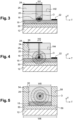
- Figure 3 is a cross-sectional view of the photonic device 10 along section AA in Figure 2 showing the main portion 34.
- the interface 30 covers entirely the substrate 12.
- the inferior cladding 18 covers entirely the interface 30.
- the active core 16 and the superior cladding 20 are superimposed to form an assembly with a rectangular cross-section and are laid approximately in the center of the inferior cladding 18.
- the active core 16 and the superior cladding 20 have the same width W1.
- the width W1 is approximately seven times smaller than the inferior cladding's 18 width.
- a typical width W1 is between 0.8 to 5 ⁇ m with most probable range between 1 and 2 ⁇ m.
- the active core 16 has a typical thickness of 100 to 600 nm.
- the active core 16 has a higher refractive index than the inferior cladding 18, and than the superior cladding 20.
- the first electrical connection 22 is a metal plate placed to the right of regrown layer 26 in figure 3 and covering a portion of the inferior cladding 18 of about 10 ⁇ m (micrometres).
- the regrown layer 26 has been regrown vertically on top of the inferior cladding 18 over a width W2.
- the regrown layer 26 covers the inferior cladding 18 except for the location of the active core 16 and for the location of the first electrical connection 22.
- the regrown layer 26 extends on either side of the active core 16 and of the superior cladding 20 over the entire height of the assembly formed by the active core 16 and the superior cladding 20.
- the regrown layer 26 can have a thickness of 1 to 4 ⁇ m, with most typical value in the range 2-3 ⁇ m.
- the thickness of the regrown layer depends on the thickness of the PIN junction, in particular, the superior cladding 20 thickness.
- the second electrical connection 24 is a plate placed on the top left of the photonic device 10 in figure 3 and covering the left part of the regrown layer 26 and the superior cladding 20.
- Figure 4 is a cross-sectional view of the photonic device 10 along section BB in Figure 2 showing the proximal end 46 of the transition portion 38.
- the interface 30 covers entirely the substrate 12.
- the inferior cladding 18 covers entirely the interface 30.
- the device may not comprise an interface 30.
- the inferior cladding 18 may extend only under the regrown layer 26 and under the active core 16.
- the active core 16 and the superior cladding 20 are superimposed to form an assembly with a rectangular cross-section and are laid, in this example, approximately in the center of the inferior cladding 18.
- the active core 16 and the superior cladding 20 have the same width W3.
- the width W3 is smaller than the width W1.
- the width W3 is sufficiently thin so that most of the light O is in the regrown layer 26.
- Typical value of W3 is below 500 nm for efficient coupling and above 100 nm for practical manufacturing. There is no lower limit except technological limit.
- the first electrical connection 22 is a plate placed to the right of the inferior cladding 18 in figure 4 and covering a portion of the inferior cladding 18.
- the regrown layer 26 has been regrown vertically on top of the inferior cladding 18 over a width W4.
- the width W4 is smaller than the width W2.
- the width W4 is approximately 4/5 of the width W2.
- the regrown layer 26 may be centred on the active core 16 and the superior cladding 20.
- the regrown layer 26 extends on either side of the active core 16 and of the superior cladding 20 over the entire height of the assembly formed by the active core 16 and the superior cladding 20.
- another portion of the interface 30, the left portion 54 has also been added on top of the inferior cladding 18, on the left of figure 4 , where the inferior cladding 30 is not covered by the regrown layer 26, nor by the active core 16, nor by the second electrical connection 22.
- the left portion 54 of the interface 30 on top of the inferior cladding 18 extends over the entire height of the assembly formed by the active core 16 and the superior cladding 20.
- the second electrical connection 24 is a plate placed on the top left of the photonic device 10 in figure 4 and covers the left portion 54 of the interface 30, the left part of the regrown layer 26 and the superior cladding 20.
- Figure 5 is a cross-sectional view of the photonic device 10 along section CC in Figure 2 showing the tip 52 of the extremal end 40.
- a lower portion 56 of the interface 30 covers entirely the substrate 12.
- the active core 16 and the superior cladding 20 are not present.
- the first and the second electrical connections 22, 24 are not present either.
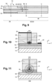
- Figure 2 shows that the transition portion 38 comprises an intermediary part 60 between the proximal end 46 and the tip 52 of the extremal end 40 in which the width 50 of the inferior cladding 18 decreases gradually, for instance substantially linearly.
- the width 50 of the inferior cladding 18 can decrease in a different way, for example exponentially, according to an arctangent function or to a polynomial function.
- the inferior cladding 18 is laid on top of the lower portion 56 of the interface 30.
- the inferior cladding 18 has a width W5 smaller than the width W6 of the substrate 12 and of the lower portion 56 of the interface 30.
- the inferior cladding 18 is centered on the lower portion 56 of the interface 30.
- the regrown layer 26 extends on the entire upper surface of the inferior cladding 18 and has the same width W5 as the inferior cladding 18.
- a typical width W5 is of 2 to 5 ⁇ m.
- the inferior cladding 18 and the regrown layer 26 form an assembly with a rectangular cross-section (e.g. square cross-section, or a nearly square cross-section) in the tip 52 of the extremal end 40.
- a rectangular cross-section e.g. square cross-section, or a nearly square cross-section
- the cross section may be a 2.5*3 ⁇ m cross section.
- the cross section may be a rectangular cross section whose smallest dimension is less than 1.5 times smaller than the longer dimension.
- the interface 30 also extends vertically on either side of the regrown layer 26 and of the inferior cladding 18.
- the interface 30 comprises the lower portion 56, a left portion 54 on the left of the regrown layer 26 and a right portion 58 on the right of the regrown layer 26.
- the left portion 54 and the right portion 58 extend over the entire height of the assembly formed by the regrown layer 26 and the inferior cladding 18.
- Figure 6 shows a second embodiment in which, in the tip 52 of the extremal end 40, the interface 30 does not extend on either side of the assembly formed by the regrown layer 26 and the inferior cladding 18.
- the assembly formed by the regrown layer 26 and the inferior cladding 18 forms a passive waveguide on the right of the photonic device 10, suitable to perform edge coupling.
- Figure 7 shows the circular mode M1 of the light O propagating in the tip 52 of the extremal end 40.
- the mode M1 has a regular shape, almost circular and have a large diameter, approximately equal to the width W5 of the regrown layer 26.
- Figure 8 horizontal and vertical cuts of the mode M1 are shown.
- the absence of the active core 16 and of the superior cladding 20 in the tip 52 of the extremal end 40 avoids the complexity of a long and very thin active waveguide consisting of the active core 16 and of the superior cladding 20. It also avoids competition between the active waveguide and the passive waveguide which allows to have a nicer mode profile.
- Figure 8 shows the power density P as a function of the mode M 1.
- the power density P has a typical shape of a wedge curve and shows no significant losses for any mode.
- An advantage of the embodiments described is the possibility to use the large passive waveguide formed by the assembly of the regrown layer 26 and the inferior cladding 18 as a low loss waveguide, which is very interesting for resonators, interferometers, filters, or light routing.
- the passive waveguide formed by the assembly of the regrown layer 26 and the inferior cladding 18 has a high index, just slightly lower than the active core 16, which allows an efficient transition between the active core 16 and the passive waveguide.
- the photonic device described allows to couple both transverse-electric (TE) and transverse-magnetic (TM) polarization.
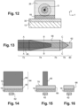
- Figure 9 shows a photonic device 10 according to a third embodiment.
- the transition portion 38 does not comprise a proximal end 46 in which the width 48 of the regrown layer 26 decreases gradually, for instance substantially linearly.
- the regrown layer 26 passes directly from a first width in the main portion 34 to a second width in the transition portion 38.
- Figure 9 is a top view of the photonic device 10, the active core 16 is not directly visible. However, the active core 16 has the same horizontal cross section as the superior cladding 20.
- the transition portion 38 does not comprise an intermediary part 60 in which the width 50 of the inferior cladding 18 decreases gradually, for instance substantially linearly.
- the inferior cladding 18 passes directly from a first width in the main portion 34 to a second width in the transition portion 38.
- Figure 10 is a cross-sectional view of the photonic device 10 along section AA in Figure 9 showing the main portion 34.
- the main portion 34 in figure 10 is the same as the main portion 34 in figure 3 .
- Figure 11 is a cross-sectional view of the photonic device 10 along section BB in Figure 9 showing the transition portion 38 between the main portion 34 and the distal part 44.
- the active core 16 and the superior cladding 20 are superimposed to form an assembly with a rectangular cross-section and are laid approximately in the center of the inferior cladding 18.
- the active core 16 and the superior cladding 20 have the same width W3.
- the width W3 is smaller than the width W1.
- the inferior cladding 18 has the same width W5 as the regrown layer 26. There is no electrical connections 22, 24.
- the interface 30 does not comprise left or right portions on the sides of the regrown layer 26.
- the inferior cladding 18 and the regrown layer 26 form an assembly with a rectangular cross section (e.g. square cross-section, or a nearly square cross-section).
- a rectangular cross section e.g. square cross-section, or a nearly square cross-section.
- the cross section may be a 2.5*3 ⁇ m cross section.
- the cross section may be a rectangular cross section whose smallest dimension is less than 1.5 times smaller than the longer dimension.
- Figure 12 is a cross-sectional view of the photonic device 10 along section CC in Figure 9 showing the tip 52 of the extremal end 40.
- the tip 52 of the extremal end 40 in figure 12 is the same as the tip 52 in figure 6 .
- the device 10 does not require coupling to a silicon waveguide in the SiO2 layer which coupling complexifies alignment and is sensitive to the SiO2 bonding thickness.
- Figures 13 to 16 show a photonic device 10 according to a fourth embodiment.
- the photonic device 10 has a silicon waveguide 62 in the interface 30.
- the photonic device 10 has an architecture to improve the coupling of the III-V passive waveguide formed by the regrown layer 26, the inferior cladding 18 and the underneath silicon waveguide 62.
- the use of a thinner regrown layer 26 improves the coupling between the III-V passive waveguide and the silicon waveguide 62 but reduces the mode size.
- a dual thickness III-V passive waveguide 64 can be implemented as shown in the fourth embodiment.
- Figure 13 is a top view of the photonic device 10 and figure 14, figure 15 and figure 16 are cross-sectional views of the photonic device 10 along respectively section AA, section BB and section CC in Figure 13 .
- the dual thickness III-V passive waveguide 64 comprises a first stage 66 corresponding to the lower part of the dual thickness III-V passive waveguide 64 and extending vertically on about a fifth of the height of the dual thickness III-V passive waveguide 64.
- the dual thickness III-V passive waveguide 64 comprises a second stage 68 and extending vertically over the rest of the dual thickness III-V passive waveguide 64 height.
- the first stage 66 and the second stage 68 have the same constant width.
- the first stage 66 keeps its constant width, but the second stage 68 is tapered.
- the first stage 66 keeps its constant width, and the second stage 68 is no more present.
- the first stage 66 is tapered, and the second stage is still not present.
- both the first stage 66 and the second stage 68 are not present. Only the silicon waveguide 62 extends in the fifth portion 80.
- An etch stop 70 can be used at the interface of the first stage 66 and the second stage 68 to obtain the desired shape of the second stage 68 without etching the first stage 66.
- the etch stop 70 is for example a AllnAs layer.
- the silicon waveguide 62 is optional and can be either removed everywhere or kept only in some predefined parts destinated to have silicon photonic functionality.
- the photonic device 10 can be obtained using the following method of fabrication comprising the following steps:
- III-V and silicon as described in the fourth embodiment is very advantageous. Indeed, silicon photonic technology is a growing field within photonics due to its very efficient manufacturing process, based on Complementary Metal Oxide Semiconductor (CMOS). Besides, silicon waveguides can be integrated with low loss. However, no light emission or amplification is possible on silicon, and, for ultimate performances, III-V modulator and photodiode are better than their silicon counterpart.
- CMOS Complementary Metal Oxide Semiconductor
- III-V modulator and photodiode are better than their silicon counterpart.
- the fourth embodiment allows the integration of III-V components into silicon waveguides.
- the photonic device may be integrated in:
Landscapes
- Physics & Mathematics (AREA)
- Condensed Matter Physics & Semiconductors (AREA)
- General Physics & Mathematics (AREA)
- Electromagnetism (AREA)
- Optics & Photonics (AREA)
- Geometry (AREA)
- Optical Integrated Circuits (AREA)
Priority Applications (1)
| Application Number | Priority Date | Filing Date | Title |
|---|---|---|---|
| EP23307208.1A EP4572039A1 (de) | 2023-12-14 | 2023-12-14 | Semi-isolierender bündelquerschnitt umwandler mit grosser brechzahl zur optischen kopplung von iii-v an silizium-heterointegrierte schaltungen |
Applications Claiming Priority (1)
| Application Number | Priority Date | Filing Date | Title |
|---|---|---|---|
| EP23307208.1A EP4572039A1 (de) | 2023-12-14 | 2023-12-14 | Semi-isolierender bündelquerschnitt umwandler mit grosser brechzahl zur optischen kopplung von iii-v an silizium-heterointegrierte schaltungen |
Publications (1)
| Publication Number | Publication Date |
|---|---|
| EP4572039A1 true EP4572039A1 (de) | 2025-06-18 |
Family
ID=89535840
Family Applications (1)
| Application Number | Title | Priority Date | Filing Date |
|---|---|---|---|
| EP23307208.1A Pending EP4572039A1 (de) | 2023-12-14 | 2023-12-14 | Semi-isolierender bündelquerschnitt umwandler mit grosser brechzahl zur optischen kopplung von iii-v an silizium-heterointegrierte schaltungen |
Country Status (1)
| Country | Link |
|---|---|
| EP (1) | EP4572039A1 (de) |
Citations (4)
| Publication number | Priority date | Publication date | Assignee | Title |
|---|---|---|---|---|
| US20030095751A1 (en) * | 2001-11-17 | 2003-05-22 | Rogers David Carnegie | Semiconductor optical devices and methods of making them |
| EP2809540A1 (de) | 2012-02-03 | 2014-12-10 | Conversant Intellectual Property Management Inc. | Vorrichtung und verfahren zur stromversorgung eines hybridfahrzeugs |
| US20150270684A1 (en) * | 2014-03-19 | 2015-09-24 | Kabushiki Kaisha Toshiba | Semiconductor laser device |
| US20200379174A1 (en) * | 2019-05-28 | 2020-12-03 | Ciena Corporation | Monolithically Integrated Gain Element |
-
2023
- 2023-12-14 EP EP23307208.1A patent/EP4572039A1/de active Pending
Patent Citations (4)
| Publication number | Priority date | Publication date | Assignee | Title |
|---|---|---|---|---|
| US20030095751A1 (en) * | 2001-11-17 | 2003-05-22 | Rogers David Carnegie | Semiconductor optical devices and methods of making them |
| EP2809540A1 (de) | 2012-02-03 | 2014-12-10 | Conversant Intellectual Property Management Inc. | Vorrichtung und verfahren zur stromversorgung eines hybridfahrzeugs |
| US20150270684A1 (en) * | 2014-03-19 | 2015-09-24 | Kabushiki Kaisha Toshiba | Semiconductor laser device |
| US20200379174A1 (en) * | 2019-05-28 | 2020-12-03 | Ciena Corporation | Monolithically Integrated Gain Element |
Non-Patent Citations (2)
| Title |
|---|
| CLAIRE BESANCON: "AlGaInAs Multi-Quantum Well Lasers on Silicon-on-Insulator Photonic Integrated Circuits Based on InP-Seed-Bonding and Epitaxial Regrowth", APPLIED SCIENCES, vol. 12, no. 1, 28 December 2021 (2021-12-28), pages 263, XP093162581, ISSN: 2076-3417, DOI: 10.3390/app12010263 * |
| M. LAMPONI: "Low-Threshold Heterogeneously Integrated InP/SOI Lasers With a Double Adiabatic Taper Coupler", IEEE PHOTONICS TECHNOLOGY LETTERS, vol. 24, no. 1, 1 January 2012 (2012-01-01), USA, pages 76 - 78, XP093162589, ISSN: 1041-1135, DOI: 10.1109/LPT.2011.2172791 * |
Similar Documents
| Publication | Publication Date | Title |
|---|---|---|
| US6162655A (en) | Method of fabricating an expanded beam optical waveguide device | |
| CN111817131B (zh) | 半导体集成光学器件以及制造半导体集成光学器件的方法 | |
| US20110243494A1 (en) | Semiconductor optical amplifier module | |
| EP1245971B1 (de) | Sich verjüngender Wellenleiter (Taper) mit lateralen strahlbegrenzenden Rippenwellenleitern | |
| US7072557B2 (en) | InP-based photonic integrated circuits with Al-containing waveguide cores and InP-based array waveguide gratings (AWGs) and avalanche photodiodes (APDs) and other optical components containing an InAlGaAs waveguide core | |
| US7454111B2 (en) | Optical device of waveguide type and its production method | |
| EP0898348A1 (de) | Optischer Halbleiterverstärker | |
| JP2010263153A (ja) | 半導体集積光デバイス及びその作製方法 | |
| CN112072470B (zh) | 多波长激光器阵列及其制作方法 | |
| US5863809A (en) | Manufacture of planar photonic integrated circuits | |
| KR100321525B1 (ko) | 반도체광디바이스및그제조방법 | |
| EP4379435A1 (de) | Heterogen integrierte photonische plattform mit kurzer wellenlänge | |
| CN120742484A (zh) | 一种光子集成器件的制备方法及结构 | |
| EP4572039A1 (de) | Semi-isolierender bündelquerschnitt umwandler mit grosser brechzahl zur optischen kopplung von iii-v an silizium-heterointegrierte schaltungen | |
| US20030143769A1 (en) | Method for fabricating monolithic integrated semiconductor photonic device | |
| EP2403077B1 (de) | Photonische Vorrichtung und Verfahren zur Herstellung einer photonischen Vorrichtung | |
| US10684414B1 (en) | Interconnect between different multi-quantum well waveguides in a semiconductor photonic integrated circuit | |
| US7273565B2 (en) | Method for manufacturing a photonic device and a photonic device | |
| CN119575704A (zh) | 半导体光元件、以及半导体光元件的制造方法 | |
| JPH04283704A (ja) | 半導体光導波路 | |
| US10725241B2 (en) | Asymmetrical spot-size converter and method of manufacturing spot-size converter | |
| JP2006091880A (ja) | アクティブ構造体に接続する低寄生容量の突合せ接合型パッシブ導波路装置及び方法 | |
| CN119518414B (zh) | 一种单片集成激光器芯片及其制备方法和应用 | |
| JP3275858B2 (ja) | 化合物半導体素子の製造方法 | |
| JP2002023205A (ja) | 方向性結合器、光変調器、及び波長選択器 |
Legal Events
| Date | Code | Title | Description |
|---|---|---|---|
| PUAI | Public reference made under article 153(3) epc to a published international application that has entered the european phase |
Free format text: ORIGINAL CODE: 0009012 |
|
| STAA | Information on the status of an ep patent application or granted ep patent |
Free format text: STATUS: THE APPLICATION HAS BEEN PUBLISHED |
|
| AK | Designated contracting states |
Kind code of ref document: A1 Designated state(s): AL AT BE BG CH CY CZ DE DK EE ES FI FR GB GR HR HU IE IS IT LI LT LU LV MC ME MK MT NL NO PL PT RO RS SE SI SK SM TR |
|
| STAA | Information on the status of an ep patent application or granted ep patent |
Free format text: STATUS: REQUEST FOR EXAMINATION WAS MADE |
|
| 17P | Request for examination filed |
Effective date: 20251006 |