EP4422379A2 - Zwei- und dreischichtige grenzflächenschichten in perowskitmaterialvorrichtungen - Google Patents
Zwei- und dreischichtige grenzflächenschichten in perowskitmaterialvorrichtungen Download PDFInfo
- Publication number
- EP4422379A2 EP4422379A2 EP24187494.0A EP24187494A EP4422379A2 EP 4422379 A2 EP4422379 A2 EP 4422379A2 EP 24187494 A EP24187494 A EP 24187494A EP 4422379 A2 EP4422379 A2 EP 4422379A2
- Authority
- EP
- European Patent Office
- Prior art keywords
- layer
- lead
- lead halide
- layers
- perovskite
- Prior art date
- Legal status (The legal status is an assumption and is not a legal conclusion. Google has not performed a legal analysis and makes no representation as to the accuracy of the status listed.)
- Pending
Links
Images






Classifications
-
- H—ELECTRICITY
- H01—ELECTRIC ELEMENTS
- H01G—CAPACITORS; CAPACITORS, RECTIFIERS, DETECTORS, SWITCHING DEVICES, LIGHT-SENSITIVE OR TEMPERATURE-SENSITIVE DEVICES OF THE ELECTROLYTIC TYPE
- H01G9/00—Electrolytic capacitors, rectifiers, detectors, switching devices, light-sensitive or temperature-sensitive devices; Processes of their manufacture
- H01G9/20—Light-sensitive devices
- H01G9/2027—Light-sensitive devices comprising an oxide semiconductor electrode
- H01G9/2031—Light-sensitive devices comprising an oxide semiconductor electrode comprising titanium oxide, e.g. TiO2
-
- H—ELECTRICITY
- H10—SEMICONDUCTOR DEVICES; ELECTRIC SOLID-STATE DEVICES NOT OTHERWISE PROVIDED FOR
- H10K—ORGANIC ELECTRIC SOLID-STATE DEVICES
- H10K85/00—Organic materials used in the body or electrodes of devices covered by this subclass
- H10K85/50—Organic perovskites; Hybrid organic-inorganic perovskites [HOIP], e.g. CH3NH3PbI3
-
- H—ELECTRICITY
- H01—ELECTRIC ELEMENTS
- H01G—CAPACITORS; CAPACITORS, RECTIFIERS, DETECTORS, SWITCHING DEVICES, LIGHT-SENSITIVE OR TEMPERATURE-SENSITIVE DEVICES OF THE ELECTROLYTIC TYPE
- H01G9/00—Electrolytic capacitors, rectifiers, detectors, switching devices, light-sensitive or temperature-sensitive devices; Processes of their manufacture
- H01G9/20—Light-sensitive devices
- H01G9/2059—Light-sensitive devices comprising an organic dye as the active light absorbing material, e.g. adsorbed on an electrode or dissolved in solution
-
- H—ELECTRICITY
- H10—SEMICONDUCTOR DEVICES; ELECTRIC SOLID-STATE DEVICES NOT OTHERWISE PROVIDED FOR
- H10F—INORGANIC SEMICONDUCTOR DEVICES SENSITIVE TO INFRARED RADIATION, LIGHT, ELECTROMAGNETIC RADIATION OF SHORTER WAVELENGTH OR CORPUSCULAR RADIATION
- H10F77/00—Constructional details of devices covered by this subclass
- H10F77/10—Semiconductor bodies
- H10F77/12—Active materials
-
- H—ELECTRICITY
- H10—SEMICONDUCTOR DEVICES; ELECTRIC SOLID-STATE DEVICES NOT OTHERWISE PROVIDED FOR
- H10K—ORGANIC ELECTRIC SOLID-STATE DEVICES
- H10K30/00—Organic devices sensitive to infrared radiation, light, electromagnetic radiation of shorter wavelength or corpuscular radiation
- H10K30/10—Organic devices sensitive to infrared radiation, light, electromagnetic radiation of shorter wavelength or corpuscular radiation comprising heterojunctions between organic semiconductors and inorganic semiconductors
- H10K30/15—Sensitised wide-bandgap semiconductor devices, e.g. dye-sensitised TiO2
-
- H—ELECTRICITY
- H10—SEMICONDUCTOR DEVICES; ELECTRIC SOLID-STATE DEVICES NOT OTHERWISE PROVIDED FOR
- H10K—ORGANIC ELECTRIC SOLID-STATE DEVICES
- H10K30/00—Organic devices sensitive to infrared radiation, light, electromagnetic radiation of shorter wavelength or corpuscular radiation
- H10K30/80—Constructional details
- H10K30/81—Electrodes
- H10K30/82—Transparent electrodes, e.g. indium tin oxide [ITO] electrodes
-
- H—ELECTRICITY
- H01—ELECTRIC ELEMENTS
- H01G—CAPACITORS; CAPACITORS, RECTIFIERS, DETECTORS, SWITCHING DEVICES, LIGHT-SENSITIVE OR TEMPERATURE-SENSITIVE DEVICES OF THE ELECTROLYTIC TYPE
- H01G9/00—Electrolytic capacitors, rectifiers, detectors, switching devices, light-sensitive or temperature-sensitive devices; Processes of their manufacture
- H01G9/20—Light-sensitive devices
- H01G9/2027—Light-sensitive devices comprising an oxide semiconductor electrode
- H01G9/2036—Light-sensitive devices comprising an oxide semiconductor electrode comprising mixed oxides, e.g. ZnO covered TiO2 particles
-
- H—ELECTRICITY
- H01—ELECTRIC ELEMENTS
- H01G—CAPACITORS; CAPACITORS, RECTIFIERS, DETECTORS, SWITCHING DEVICES, LIGHT-SENSITIVE OR TEMPERATURE-SENSITIVE DEVICES OF THE ELECTROLYTIC TYPE
- H01G9/00—Electrolytic capacitors, rectifiers, detectors, switching devices, light-sensitive or temperature-sensitive devices; Processes of their manufacture
- H01G9/20—Light-sensitive devices
- H01G9/2027—Light-sensitive devices comprising an oxide semiconductor electrode
- H01G9/204—Light-sensitive devices comprising an oxide semiconductor electrode comprising zinc oxides, e.g. ZnO
-
- H—ELECTRICITY
- H10—SEMICONDUCTOR DEVICES; ELECTRIC SOLID-STATE DEVICES NOT OTHERWISE PROVIDED FOR
- H10K—ORGANIC ELECTRIC SOLID-STATE DEVICES
- H10K85/00—Organic materials used in the body or electrodes of devices covered by this subclass
- H10K85/60—Organic compounds having low molecular weight
- H10K85/631—Amine compounds having at least two aryl rest on at least one amine-nitrogen atom, e.g. triphenylamine
- H10K85/633—Amine compounds having at least two aryl rest on at least one amine-nitrogen atom, e.g. triphenylamine comprising polycyclic condensed aromatic hydrocarbons as substituents on the nitrogen atom
-
- H—ELECTRICITY
- H10—SEMICONDUCTOR DEVICES; ELECTRIC SOLID-STATE DEVICES NOT OTHERWISE PROVIDED FOR
- H10K—ORGANIC ELECTRIC SOLID-STATE DEVICES
- H10K85/00—Organic materials used in the body or electrodes of devices covered by this subclass
- H10K85/60—Organic compounds having low molecular weight
- H10K85/631—Amine compounds having at least two aryl rest on at least one amine-nitrogen atom, e.g. triphenylamine
- H10K85/636—Amine compounds having at least two aryl rest on at least one amine-nitrogen atom, e.g. triphenylamine comprising heteroaromatic hydrocarbons as substituents on the nitrogen atom
-
- Y—GENERAL TAGGING OF NEW TECHNOLOGICAL DEVELOPMENTS; GENERAL TAGGING OF CROSS-SECTIONAL TECHNOLOGIES SPANNING OVER SEVERAL SECTIONS OF THE IPC; TECHNICAL SUBJECTS COVERED BY FORMER USPC CROSS-REFERENCE ART COLLECTIONS [XRACs] AND DIGESTS
- Y02—TECHNOLOGIES OR APPLICATIONS FOR MITIGATION OR ADAPTATION AGAINST CLIMATE CHANGE
- Y02E—REDUCTION OF GREENHOUSE GAS [GHG] EMISSIONS, RELATED TO ENERGY GENERATION, TRANSMISSION OR DISTRIBUTION
- Y02E10/00—Energy generation through renewable energy sources
- Y02E10/50—Photovoltaic [PV] energy
- Y02E10/542—Dye sensitized solar cells
-
- Y—GENERAL TAGGING OF NEW TECHNOLOGICAL DEVELOPMENTS; GENERAL TAGGING OF CROSS-SECTIONAL TECHNOLOGIES SPANNING OVER SEVERAL SECTIONS OF THE IPC; TECHNICAL SUBJECTS COVERED BY FORMER USPC CROSS-REFERENCE ART COLLECTIONS [XRACs] AND DIGESTS
- Y02—TECHNOLOGIES OR APPLICATIONS FOR MITIGATION OR ADAPTATION AGAINST CLIMATE CHANGE
- Y02E—REDUCTION OF GREENHOUSE GAS [GHG] EMISSIONS, RELATED TO ENERGY GENERATION, TRANSMISSION OR DISTRIBUTION
- Y02E10/00—Energy generation through renewable energy sources
- Y02E10/50—Photovoltaic [PV] energy
- Y02E10/549—Organic PV cells
Definitions
- PVs photovoltaics
- Improvements in various aspects of PV technologies compatible with organic, non-organic, and/or hybrid PVs promise to further lower the cost of both organic PVs and other PVs.
- some solar cells such as solid-state dye-sensitized solar cells, may take advantage of novel cost-effective and high-stability alternative components, such as solid-state charge transport materials (or, colloquially, "solid state electrolytes").
- solid-state charge transport materials or, colloquially, "solid state electrolytes”
- various kinds of solar cells may advantageously include interfacial and other materials that may, among other advantages, be more cost-effective and durable than conventional options currently in existence.
- the present disclosure relates generally to compositions of matter, apparatus and methods of use of materials in photovoltaic cells in creating electrical energy from solar radiation. More specifically, this disclosure relates to photoactive and other compositions of matter, as well as apparatus, methods of use, and formation of such compositions of matter.
- compositions of matter may include, for example, hole-transport materials, and/or materials that may be suitable for use as, e.g., interfacial layers (IFLs), dyes, and/or other elements of PV devices.
- IFLs interfacial layers
- Such compounds may be deployed in a variety of PV devices, such as heterojunction cells (e.g., bilayer and bulk), hybrid cells (e.g., organics with CHsNHsPbIs, ZnO nanorods or PbS quantum dots), and DSSCs (dye-sensitized solar cells).
- DSSCs exist in three forms: solvent-based electrolytes, ionic liquid electrolytes, and solid-state hole transporters (or solid-state DSSCs, i.e., SS-DSSCs).
- SS-DSSC structures may be substantially free of electrolyte, containing rather hole-transport materials such as spiro-OMeTAD, CsSnI 3 , and other active materials.
- materials in accordance with some embodiments of the present disclosure may also advantageously be used in any organic or other electronic device, with some examples including, but not limited to: batteries, field-effect transistors (FETs), light-emitting diodes (LEDs), non-linear optical devices, memristors, capacitors, rectifiers, and/or rectifying antennas.
- FETs field-effect transistors
- LEDs light-emitting diodes
- non-linear optical devices memristors, capacitors, rectifiers, and/or rectifying antennas.
- the present disclosure may provide PV and other similar devices (e.g., batteries, hybrid PV batteries, multi-junction PVs, FETs, LEDs etc.).
- Such devices may in some embodiments include improved active material, interfacial layers, and/or one or more perovskite materials.
- a perovskite material may be incorporated into various of one or more aspects of a PV or other device.
- a perovskite material may be of the general formula CMX 3 , where: C comprises one or more cations (e.g., an amine, ammonium, a Group 1 metal, a Group 2 metal, and/or other cations or cation-like compounds); M comprises one or more metals (example s including Fe, Co, Ni, Cu, Sn, Pb, Bi, Ge, Ti, and Zr); and X comprises one or more anions.
- C comprises one or more cations (e.g., an amine, ammonium, a Group 1 metal, a Group 2 metal, and/or other cations or cation-like compounds)
- M comprises one or more metals (example s including Fe, Co, Ni, Cu, Sn, Pb, Bi, Ge, Ti, and Zr)
- X comprises one or more anions.
- an example PV architecture may be substantially of the form substrate-anode-IFL-active layer-IFL-cathode.
- the active layer of some embodiments may be photoactive, and/or it may include photoactive material.
- Other layers and materials may be utilized in the cell as is known in the art.
- active layer is in no way meant to restrict or otherwise define, explicitly or implicitly, the properties of any other layer - for instance, in some embodiments, either or both IFLs may also be active insofar as they may be semiconducting.
- a stylized generic PV cell 2610 is depicted, illustrating the highly interfacial nature of some layers within the PV.
- the PV 2610 represents a generic architecture applicable to several PV devices, such as perovskite material PV embodiments.
- the PV cell 2610 includes a transparent layer 2612 of glass (or material similarly transparent to solar radiation) which allows solar radiation 2614 to transmit through the layer.
- the transparent layer of some embodiments may also be referred to as a substrate (e.g., as with substrate layer 1507 of FIG. 1 ), and it may comprise any one or more of a variety of rigid or flexible materials such as: glass, polyethylene, PET, Kapton, quartz, aluminum foil, gold foil, or steel.
- the photoactive layer 2616 is composed of electron donor or p -type material 2618 , and/or an electron acceptor or n -type material 2620, and/or an ambipolar semiconductor, which exhibits both p - and n -type material characteristics.
- the active layer or, as depicted in FIG. 4 , the photo-active layer 2616 is sandwiched between two electrically conductive electrode layers 2622 and 2624.
- the electrode layer 2622 is a tin-doped indium oxide (ITO material).
- ITO material tin-doped indium oxide
- an active layer of some embodiments need not necessarily be photoactive, although in the device shown in FIG. 4 , it is.
- the electrode layer 2624 is an aluminum material. Other materials may be used as is known in the art.
- the cell 2610 also includes an interfacial layer (IFL) 2626 , shown in the example of FIG. 4 as a ZnO material.
- the IFL may assist in charge separation.
- the IFL 2626 may comprise an organic compound according to the present disclosure as a self-assembled monolayer (SAM) or as a thin film.
- the IFL 2626 may comprise a multi-layer IFL, which is discussed in greater detail below.
- the IFL 2627 adjacent to electrode 2624 may also or instead comprise an organic compound according to the present disclosure as a self-assembled monolayer (SAM) or as a thin film.
- the IFL 2627 adjacent to electrode 2624 may also or instead comprise a multi-layer IFL (again, discussed in greater detail below).
- An IFL may be semiconducting in character and may be either p -type or n -type, or it may be dielectric in character.
- the IFL on the cathode side of the device e.g., IFL 2627 as shown in FIG. 4
- the IFL on the anode side of the device e.g., IFL 2626 as shown in FIG. 4
- the cathode-side IFL may be n -type and the anode-side IFL may be p -type.
- the cell 2610 is attached to leads 2630 and a discharge unit 2632, such as a battery.
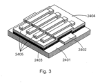
- FIG. 3 depicts a stylized BHJ device design, and includes: glass substrate 2401 ; ITO (tin-doped indium oxide) electrode 2402 ; interfacial layer (IFL) 2403 ; photoactive layer 2404 ; and LiF/Al cathodes 2405 .
- the materials of BHJ construction referred to are mere examples; any other BHJ construction known in the art may be used consistent with the present disclosure.
- the photoactive layer 2404 may comprise any one or more materials that the active or photoactive layer 2616 of the device of FIG. 4 may comprise.
- FIG. 1 is a simplified illustration of DSSC PVs according to some embodiments, referred to here for purposes of illustrating assembly of such example PVs.
- An example DSSC as shown in FIG. 1 may be constructed according to the following: electrode layer 1506 (shown as fluorine-doped tin oxide, FTO) is deposited on a substrate layer 1507 (shown as glass).
- Mesoporous layer ML 1505 (which may in some embodiments be TiO 2 ) is deposited onto the electrode layer 1506 , then the photoelectrode (so far comprising substrate layer 1507 , electrode layer 1506 , and mesoporous layer 1505 ) is soaked in a solvent (not shown) and dye 1504.
- a separate counter-electrode is made comprising substrate layer 1501 (also shown as glass) and electrode layer 1502 (shown as Pt/FTO).
- the photoelectrode and counter-electrode are combined, sandwiching the various layers 1502 - 1506 between the two substrate layers 1501 and 1507 as shown in FIG. 1 , and allowing electrode layers 1502 and 1506 to be utilized as a cathode and anode, respectively.
- a layer of electrolyte 1503 is deposited either directly onto the completed photoelectrode after dye layer 1504 or through an opening in the device, typically a hole pre-drilled by sand-blasting in the counter-electrode substrate 1501.
- the cell may also be attached to leads and a discharge unit, such as a battery (not shown).
- a discharge unit such as a battery (not shown).
- Substrate layer 1507 and electrode layer 1506 , and/or substrate layer 1501 and electrode layer 1502 should be of sufficient transparency to permit solar radiation to pass through to the photoactive dye 1504 .
- the counter-electrode and/or photoelectrode may be rigid, while in others either or both may be flexible.
- the substrate layers of various embodiments may comprise any one or more of: glass, polyethylene, PET, Kapton, quartz, aluminum foil, gold foil, and steel.
- a DSSC may further include a light harvesting layer 1601 , as shown in FIG. 2 , to scatter incident light in order to increase the light's path length through the photoactive layer of the device (thereby increasing the likelihood the light is absorbed in the photoactive layer).
- Solid-state DSSCs may provide advantages such as lack of leakage and/or corrosion issues that may affect DSSCs comprising liquid electrolytes.
- a solid-state charge carrier may provide faster device physics (e.g., faster charge transport).
- solid-state electrolytes may, in some embodiments, be photoactive and therefore contribute to power derived from a solid-state DSSC device.
- FIG. 5 is a stylized schematic of a typical solid state DSSC.
- an active layer comprised of first and second active (e.g., conducting and/or semi-conducting) material ( 2810 and 2815 , respectively) is sandwiched between electrodes 2805 and 2820 (shown in FIG. 5 as Pt/FTO and FTO, respectively).
- the first active material 2810 is p -type active material, and comprises a solid-state electrolyte.
- the first active material 2810 may comprise an organic material such as spiro-OMeTAD and/or poly(3-hexylthiophene), an inorganic binary, ternary, quaternary, or greater complex, any solid semiconducting material, or any combination thereof.
- the first active material may additionally or instead comprise an oxide and/or a sulfide, and/or a selenide, and/or an iodide (e.g., CsSnI 3 ).
- the first active material of some embodiments may comprise solid-state p -type material, which may comprise copper indium sulfide, and in some embodiments, it may comprise copper indium gallium selenide.
- the second active material 2815 shown in FIG. 5 is n -type active material and comprises TiO 2 coated with a dye.
- the second active material may likewise comprise an organic material such as spiro-OMeTAD, an inorganic binary, ternary, quaternary, or greater complex, or any combination thereof.
- the second active material may comprise an oxide such as alumina, and/or it may comprise a sulfide, and/or it may comprise a selenide.
- the second active material may comprise copper indium sulfide, and in some embodiments, it may comprise copper indium gallium selenide metal.
- the second active material 2815 of some embodiments may constitute a mesoporous layer.
- first and second active materials 2810 and 2815 may be photoactive.
- the second active material may comprise a solid electrolyte.
- the PV device may lack an effective amount of liquid electrolyte.
- a solid state layer e.g., first active material comprising solid electrolyte
- the second active material e.g., TiO 2 (or other mesoporous material) as shown in FIG. 5
- coated with a dye may be p -type semiconducting (as opposed to the n -type semiconducting shown in, and discussed with respect to, FIG. 5 ).
- Substrate layers 2801 and 2825 form the respective external top and bottom layers of the example cell of FIG. 5 .
- These layers may comprise any material of sufficient transparency to permit solar radiation to pass through to the active/photoactive layer comprising dye, first and second active and/or photoactive material 2810 and 2815, such as glass, polyethylene, PET, Kapton, quartz, aluminum foil, gold foil, and/or steel.
- electrode 2805 (shown as Pt/FTO) is the cathode
- electrode 2820 is the anode.
- solar radiation passes through substrate layer 2825 and electrode 2820 into the active layer, whereupon at least a portion of the solar radiation is absorbed so as to produce one or more excitons to enable electrical generation.
- Various embodiments of the present disclosure provide improved materials and/or designs in various aspects of solar cell and other devices, including among other things, active materials (including hole-transport and/or electron-transport layers), interfacial layers, and overall device design.
- active materials including hole-transport and/or electron-transport layers
- interfacial layers including interfacial layers, and overall device design.
- the present disclosure provides advantageous materials and designs of one or more interfacial layers within a PV, including thin-coat IFLs.
- Thin-coat IFLs may be employed in one or more IFLs of a PV according to various embodiments discussed herein.
- one or more IFLs may comprise a photoactive organic compound of the present disclosure as a self-assembled monolayer (SAM) or as a thin film.
- SAM self-assembled monolayer
- a photoactive organic compound of the present disclosure may comprise a binding group through which it may be covalently or otherwise bound to the surface of either or both of the anode and cathode.
- the thin-coat IFLs and methods of coating them onto TiO 2 previously discussed may, in some embodiments, be employed in DSSCs comprising liquid electrolytes.
- the DSSC of FIG. 1 could further comprise a thin-coat IFL as described above coated onto the mesoporous layer 1505 (that is, the thin-coat IFL would be inserted between mesoporous layer 1505 and dye 1504 ).
- multiple IFLs made from different materials may be arranged adjacent to each other to form a composite IFL. This configuration may involve two different IFLs, three different IFLs, or an even greater number of different IFLs.
- the resulting multi-layer IFL or composite IFL may be used in lieu of a single-material IFL.
- a composite IFL may be used as IFL 2626 and/or as IFL 2627 in cell 2610 , shown in the example of FIG. 4 . While the composite IFL differs from a single-material IFL, the assembly of a perovskite material PV cell having multi-layer IFLs is not substantially different than the assembly of a perovskite material PV cell having only single-material IFLs.
- the composite IFL may be made using any of the materials discussed herein as suitable for an IFL.
- the IFL comprises a layer of Al 2 O 3 and a layer of ZnO or M:ZnO (doped ZnO, e.g., Be:ZnO, Mg:ZnO, Ca:ZnO, Sr:ZnO, Ba:ZnO, Sc:ZnO, Y:ZnO, Nb:ZnO).
- the IFL comprises a layer of ZrO 2 and a layer of ZnO or M:ZnO.
- the IFL comprises multiple layers.
- a multi-layer IFL generally has a conductor layer, a dielectric layer, and a semi-conductor layer.
- the layers may repeat, for example, a conductor layer, a dielectric layer, a semi-conductor layer, a dielectric layer, and a semi-conductor layer.
- Arranging two or more adjacent IFLs as a composite IFL may outperform a single IFL in perovskite material PV cells where attributes from each IFL material may be leveraged in a single IFL.
- ITO is a conducting electrode
- Al 2 O 3 is a dielectric material
- ZnO is a n-type semiconductor
- ZnO acts as an electron acceptor with well performing electron transport properties (e.g., mobility).
- Al 2 O 3 is a physically robust material that adheres well to ITO, homogenizes the surface by capping surface defects (e.g., charge traps), and improves device diode characteristics through suppression of dark current.
- FIG. 11 is a stylized diagram of a perovskite material device 4500 according to some embodiments. Although various components of the device 4500 are illustrated as discrete layers comprising contiguous material, it should be understood that FIG. 11 is a stylized diagram; thus, embodiments in accordance with it may include such discrete layers, and/or substantially intermixed, non-contiguous layers, consistent with the usage of "layers" previously discussed herein.
- the device 4500 includes first and second substrates 4501 and 4508 .
- a first electrode (e.g., ITO) 4502 is disposed upon an inner surface of the first substrate 4501
- a second electrode (e.g., Ag) 4507 is disposed on an inner surface of the second substrate 4508 .
- the active layer 4550 is sandwiched between the two electrodes 4502 and 4507 .
- the active layer 4550 includes a composite IFL comprising a first IFL (e.g., Al 2 O 3 ) 4503 and a second IFL (e.g., ZnO) 4504, a photoactive material (e.g., MAPbI 3 ) 4505, and a charge transport layer (e.g., Spiro-OMeTAD) 4506 .
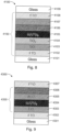
- FIGS. 13-20 are stylized diagrams of perovskite material devices according to some embodiments. Although various components of the devices are illustrated as discrete layers comprising contiguous material, it should be understood that FIGS. 13-18 are stylized diagrams; thus, embodiments in accordance with them may include such discrete layers, and/or substantially intermixed, non-contiguous layers, consistent with the usage of "layers" previously discussed herein.
- the example devices include layers and materials described throughout this disclosure.
- FIG. 13 is a stylized diagram of a perovskite material device 6100 according to some embodiments. Although various components of the device 6100 are illustrated as discrete layers comprising contiguous material, it should be understood that FIG. 13 is a stylized diagram; thus, embodiments in accordance with it may include such discrete layers, and/or substantially intermixed, non-contiguous layers, consistent with the usage of "layers" previously discussed herein.
- the device 6100 includes a substrate (e.g., Glass) 6101.
- a first electrode (e.g., ITO) 6102 is disposed upon an inner surface of the substrate 6101, and a second electrode (e.g., Ag) 6107 is disposed on top of an active layer 6150 that is sandwiched between the two electrodes 6102 and 6107 .
- the active layer 6150 includes a composite IFL comprising a first IFL (e.g., Al 2 O 3 ) 6103 and a second IFL (e.g., ZnO) 6104, a photoactive material (e.g., MAPbI 3 ) 6105, and a charge transport layer (e.g., Spiro-OMeTAD) 6106 .
- FIG. 14 is a stylized diagram of a perovskite material device 6200 according to some embodiments. Although various components of the device 6200 are illustrated as discrete layers comprising contiguous material, it should be understood that FIG. 14 is a stylized diagram; thus, embodiments in accordance with it may include such discrete layers, and/or substantially intermixed, non-contiguous layers, consistent with the usage of "layers" previously discussed herein.
- the device 6200 includes a substrate (e.g., Glass) 6201.
- a first electrode (e.g., ITO) 6202 is disposed upon an inner surface of the substrate 6201, and a second electrode (e.g., Ag) 6206 is disposed on top of an active layer 6250 that is sandwiched between the two electrodes 6202 and 6206 .
- the active layer 6250 includes an IFL (e.g., Y:ZnO) 6203 , a photoactive material (e.g., MAPbI 3 ) 6204 , and a charge transport layer (e.g., P3HT) 6205 .
- FIG. 15 is a stylized diagram of a perovskite material device 6300 according to some embodiments. Although various components of the device 6300 are illustrated as discrete layers comprising contiguous material, it should be understood that FIG. 15 is a stylized diagram; thus, embodiments in accordance with it may include such discrete layers, and/or substantially intermixed, non-contiguous layers, consistent with the usage of "layers" previously discussed herein.
- the device 6300 includes a substrate (e.g., Glass) 6301 .
- a first electrode (e.g., ITO) 6302 is disposed upon an inner surface of the substrate 6301 , and a second electrode (e.g., Ag) 6309 is disposed on top of an active layer 6350 that is sandwiched between the two electrodes 6302 and 6309.
- the active layer 6350 includes a composite IFL comprising a first IFL (e.g., Al 2 O 3 ) 6303, a second IFL (e.g., ZnO) 6304 , a third IFL (e.g., Al 2 O 3 ) 6305 , and a fourth IFL (e.g., ZnO) 6306 , a photoactive material (e.g., MAPbI 3 ) 6307 , and a charge transport layer (e.g., PCDTBT) 6308 .
- a composite IFL comprising a first IFL (e.g., Al 2 O 3 ) 6303, a second IFL (e.g., ZnO) 6304 , a third IFL (e.g., Al 2 O 3 ) 6305 , and a fourth IFL (e.g., ZnO) 6306 , a photoactive material (e.g., MAPbI 3 ) 6307 , and a
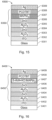
- FIG. 16 is a stylized diagram of a perovskite material device 6400 according to some embodiments. Although various components of the device 6400 are illustrated as discrete layers comprising contiguous material, it should be understood that FIG. 16 is a stylized diagram; thus, embodiments in accordance with it may include such discrete layers, and/or substantially intermixed, non-contiguous layers, consistent with the usage of "layers" previously discussed herein.
- the device 6400 includes a substrate (e.g., Glass) 6401.
- a first electrode (e.g., ITO) 6402 is disposed upon an inner surface of the substrate 6401 , and a second electrode (e.g., Ag) 6409 is disposed on top of an active layer 6450 that is sandwiched between the two electrodes 6402 and 6409.
- the active layer 6450 includes a composite IFL comprising a first IFL (e.g., Al 2 O 3 ) 6403 , a second IFL (e.g., ZnO) 6404 , a third IFL (e.g., Al 2 O 3 ) 6405 , and a fourth IFL (e.g., ZnO) 6406 , a photoactive material (e.g., 5-AVA ⁇ HCL:MAPbI 3 ) 6407 , and a charge transport layer (e.g., PCDTBT) 6408.
- a composite IFL comprising a first IFL (e.g., Al 2 O 3 ) 6403 , a second IFL (e.g., ZnO) 6404 , a third IFL (e.g., Al 2 O 3 ) 6405 , and a fourth IFL (e.g., ZnO) 6406 , a photoactive material (e.g., 5-AVA ⁇ HCL:MAPbI 3 )
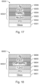
- FIG. 17 is a stylized diagram of a perovskite material device 6500 according to some embodiments. Although various components of the device 6500 are illustrated as discrete layers comprising contiguous material, it should be understood that FIG. 17 is a stylized diagram; thus, embodiments in accordance with it may include such discrete layers, and/or substantially intermixed, non-contiguous layers, consistent with the usage of "layers" previously discussed herein.
- the device 6500 includes a substrate (e.g., Glass) 6501 .
- a first electrode (e.g., ITO) 6502 is disposed upon an inner surface of the substrate 6501 , and a second electrode (e.g., Ag) 6506 is disposed on top of an active layer 6550 that is sandwiched between the two electrodes 6502 and 6506 .
- the active layer 6550 includes an IFL (e.g., Nb:ZnO) 6503 , a photoactive material (e.g., FAPbI 3 ) 6504 , and a charge transport layer (e.g., P3HT) 6505 .
- FIG. 18 is a stylized diagram of a perovskite material device 6600 according to some embodiments. Although various components of the device 6600 are illustrated as discrete layers comprising contiguous material, it should be understood that FIG. 18 is a stylized diagram; thus, embodiments in accordance with it may include such discrete layers, and/or substantially intermixed, non-contiguous layers, consistent with the usage of "layers" previously discussed herein.
- the device 6600 includes a substrate (e.g., Glass) 6601 .
- a first electrode (e.g., ITO) 6602 is disposed upon an inner surface of the substrate 6601
- a second electrode (e.g., Ag) 6606 is disposed on top of an active layer 6650 that is sandwiched between the two electrodes 6602 and 6606 .
- the active layer 6650 includes an IFL (e.g., Y:ZnO) 6603 , a photoactive material (e.g., CHP;MAPbI 3 ) 6604 , and a charge transport layer (e.g., P3HT) 6605.
- IFL e.g., Y:ZnO
- a photoactive material e.g., CHP;MAPbI 3
- P3HT charge transport layer
- FIG. 19 is a stylized diagram of a perovskite material device 6700 according to some embodiments. Although various components of the device 6700 are illustrated as discrete layers comprising contiguous material, it should be understood that FIG. 19 is a stylized diagram; thus, embodiments in accordance with it may include such discrete layers, and/or substantially intermixed, non-contiguous layers, consistent with the usage of "layers" previously discussed herein.
- the device 6700 includes a substrate (e.g., Glass) 6701 .
- a first electrode (e.g., ITO) 6702 is disposed upon an inner surface of the substrate 6701
- a second electrode (e.g., Al) 6707 is disposed on top of an active layer 6750 that is sandwiched between the two electrodes 6702 and 6707 .
- the active layer 6750 includes an IFL (e.g., SrTiOs) 6703 a photoactive material (e.g., FAPbI 3 ) 6704 , a first charge transport layer (e.g., P3HT) 6705 , and a second charge transport layer (e.g., MoOx) 6706 .
- FIG. 20 is a stylized diagram of a perovskite material device 6800 according to some embodiments. Although various components of the device 6800 are illustrated as discrete layers comprising contiguous material, it should be understood that FIG. 16 is a stylized diagram; thus, embodiments in accordance with it may include such discrete layers, and/or substantially intermixed, non-contiguous layers, consistent with the usage of "layers" previously discussed herein.
- the device 6800 includes a substrate (e.g., Glass) 6801.
- a first electrode (e.g., ITO) 6802 is disposed upon an inner surface of the substrate 6801, and a second electrode (e.g., Al) 6811 is disposed on top of an active layer 6850 that is sandwiched between the two electrodes 6802 and 6811 .
- the active layer 6850 includes a composite IFL comprising a first IFL (e.g., Al 2 O 3 ) 6803 , a second IFL (e.g., ZnO) 6804 , a third IFL (e.g., Al 2 O 3 ) 6805 , a fourth IFL (e.g., ZnO) 6806 , and a fifth IFL (e.g., Al 2 O 3 ) 6807 , a photoactive material (e.g., FAPbI 3 ) 6808 , a first charge transport layer (e.g., P3HT) 6809 , and a second charge transport layer (e.g., MoOx) 6810 .
- a composite IFL comprising a first IFL (e.g., Al 2 O 3 ) 6803 , a second IFL (e.g., ZnO) 6804 , a third IFL (e.g., Al 2 O 3 )
- a perovskite material may be incorporated into various of one or more aspects of a PV or other device.
- a perovskite material may be of the general formula CMX 3 , where: C comprises one or more cations (e.g., an amine, ammonium, a Group 1 metal, a Group 2 metal, and/or other cations or cation-like compounds); M comprises one or more metals (examples including Fe, Co, Ni, Cu, Sn, Pb, Bi, Ge, Ti, and Zr); and X comprises one or more anions.
- C may include one or more organic cations.
- C may include an ammonium, an organic cation of the general formula [NR 4 ] + where the R groups may be the same or different groups.
- C may include a formamidinium, an organic cation of the general formula [R 2 NCRNR 2 ] + where the R groups may be the same or different groups.
- Formula 1 illustrates the structure of a formamidinium cation having the general formula of [R 2 NCRNR 2 ] + as described above.
- Formula 2 illustrates examples structures of several formamidinium cations that may serve as a cation "C" in a perovskite material.
- Formula 4 illustrates examples of structures of several guanidinium cations that may serve as a cation "C" in a perovskite material.
- Formula 6 illustrates examples of structures of several ethene tetramine ions that may serve as a cation "C" in a perovskite material.
- C may include an imidazolium cation, an aromatic, cyclic organic cation of the general formula [CRNRCRNRCR] + where the R groups may be the same or different groups.
- X may include one or more halides.
- X may instead or in addition include a Group 16 anion.
- the Group 16 anion may be sulfide or selenide.
- X may instead or in addition include one or more a pseudohalides (e.g., cyanide, cyanate, isocyanate, fulminate, thiocyanate, isothiocyanate, azide, tetracarbonylcobaltate, carbamoyldicyanomethanide, dicyanonitrosomethanide, dicyanamide, and tricyanomethanide).
- a pseudohalides e.g., cyanide, cyanate, isocyanate, fulminate, thiocyanate, isothiocyanate, azide, tetracarbonylcobaltate, carbamoyldicyanomethanide, dicyanonitrosomethanide, dicyanamide, and tricyanomethanide.
- each organic cation C may be larger than each metal M, and each anion X may be capable of bonding with both a cation C and a metal M.
- perovskite materials include CsSnI 3 (previously discussed herein) and Cs x Sn y I z (with x, y, and z varying in accordance with the previous discussion).
- Other examples include compounds of the general formula CsSnX 3 , where X may be any one or more of: I 3 , I 2.95 F 0.05 ; I 2 Cl; ICl 2 ; and Cl 3 .
- X may comprise any one or more of I, Cl, F, and Br in amounts such that the total ratio of X as compared to Cs and Sn results in the general stoichiometry of CsSnX 3 .
- the combined stoichiometry of the elements that constitute X may follow the same rules as I z as previously discussed with respect to Cs x Sn y I z .
- Yet other examples include compounds of the general formula RNH 3 PbX 3 , where R may be C n H 2n+1 , with n ranging from 0-10, and X may include any one or more of F, Cl, Br, and I in amounts such that the total ratio of X as compared to the cation RNH 3 and metal Pb results in the general stoichiometry of RNH 3 PbX 3 .
- R include H, alkyl chains (e.g., CH 3 , CH 3 CH 2 , CH 3 CH 2 CH 2 , and so on), and amino acids (e.g., glycine, cysteine, proline, glutamic acid, arginine, serine, histindine, 5-ammoniumvaleric acid) including alpha, beta, gamma, and greater derivatives.
- alkyl chains e.g., CH 3 , CH 3 CH 2 , CH 3 CH 2 CH 2 , and so on
- amino acids e.g., glycine, cysteine, proline, glutamic acid, arginine, serine, histindine, 5-ammoniumvaleric acid
- the present disclosure may provide composite design of PV and other similar devices (e.g., batteries, hybrid PV batteries, FETs, LEDs etc.) including one or more perovskite materials.
- one or more perovskite materials may serve as either or both of first and second active material of some embodiments (e.g., active materials 2810 and 2815 of FIG. 5 ).
- some embodiments of the present disclosure provide PV or other devices having an active layer comprising one or more perovskite materials.
- perovskite material that is, material including any one or more perovskite materials(s)
- perovskite material may serve the function(s) of any one or more components of an active layer (e.g., charge transport material, mesoporous material, photoactive material, and/or interfacial material, each of which is discussed in greater detail below).
- an active layer e.g., charge transport material, mesoporous material, photoactive material, and/or interfacial material, each of which is discussed in greater detail below.
- the same perovskite materials may serve multiple such functions, although in other embodiments, a plurality of perovskite materials may be included in a device, each perovskite material serving one or more such functions.
- whatever role a perovskite material may serve it may be prepared and/or present in a device in various states. For example, it may be substantially solid in some embodiments.
- it may be a solution (e.g., perovskite material may be dissolved in liquid and present in said liquid in its individual ionic subspecies); or it may be a suspension (e.g., of perovskite material particles).
- a solution or suspension may be coated or otherwise deposited within a device (e.g., on another component of the device such as a mesoporous, interfacial, charge transport, photoactive, or other layer, and/or on an electrode).
- Perovskite materials in some embodiments may be formed in situ on a surface of another component of a device (e.g., by vapor deposition as a thin-film solid). Any other suitable means of forming a solid or liquid layer comprising perovskite material may be employed.
- a perovskite material device may include a first electrode, a second electrode, and an active layer comprising a perovskite material, the active layer disposed at least partially between the first and second electrodes.
- the first electrode may be one of an anode and a cathode
- the second electrode may be the other of an anode and cathode.
- An active layer may include any one or more active layer components, including any one or more of: charge transport material; liquid electrolyte; mesoporous material; photoactive material (e.g., a dye, silicon, cadmium telluride, cadmium sulfide, cadmium selenide, copper indium gallium selenide, gallium arsenide, germanium indium phosphide, semiconducting polymers, other photoactive materials)); and interfacial material. Any one or more of these active layer components may include one or more perovskite materials. In some embodiments, some or all of the active layer components may be in whole or in part arranged in sub-layers.
- the active layer may comprise any one or more of: an interfacial layer including interfacial material; a mesoporous layer including mesoporous material; and a charge transport layer including charge transport material.
- photoactive material such as a dye may be coated on, or otherwise disposed on, any one or more of these layers.
- any one or more layers may be coated with a liquid electrolyte.
- an interfacial layer may be included between any two or more other layers of an active layer according to some embodiments, and/or between a layer and a coating (such as between a dye and a mesoporous layer), and/or between two coatings (such as between a liquid electrolyte and a dye), and/or between an active layer component and an electrode.
- a layer and a coating such as between a dye and a mesoporous layer
- two coatings such as between a liquid electrolyte and a dye
- Layers may in some embodiments be discrete and comprise substantially contiguous material (e.g., layers may be as stylistically illustrated in FIG. 1 ). In other embodiments, layers may be substantially intermixed (as in the case of, e.g., BHJ, hybrid, and some DSSC cells), an example of which is shown by first and second active material 2618 and 2620 within photoactive layer 2616 in FIG. 4 . In some embodiments, a device may comprise a mixture of these two kinds of layers, as is also shown by the device of FIG. 4 , which contains discrete contiguous layers 2627 , 2626, and 2622, in addition to a photoactive layer 2616 comprising intermixed layers of first and second active material 2618 and 2620 .
- any two or more layers of whatever kind may in certain embodiments be disposed adjacent to each other (and/or intermixedly with each other) in such a way as to achieve a high contact surface area.
- a layer comprising perovskite material may be disposed adjacent to one or more other layers so as to achieve high contact surface area (e.g., where a perovskite material exhibits low charge mobility).
- high contact surface area may not be necessary (e.g., where a perovskite material exhibits high charge mobility).
- a perovskite material device may optionally include one or more substrates.
- either or both of the first and second electrode may be coated or otherwise disposed upon a substrate, such that the electrode is disposed substantially between a substrate and the active layer.
- the materials of composition of devices e.g., substrate, electrode, active layer and/or active layer components
- an electrode may act as a substrate, thereby negating the need for a separate substrate.
- a perovskite material device may optionally include light-harvesting material (e.g., in a light-harvesting layer, such as Light Harvesting Layer 1601 as depicted in the example PV represented in FIG. 2 ).
- a perovskite material device may include any one or more additives, such as any one or more of the additives discussed above with respect to some embodiments of the present disclosure.
- FIG. 7 is a stylized diagram of a perovskite material device 3900 according to some embodiments. Although various components of the device 3900 are illustrated as discrete layers comprising contiguous material, it should be understood that FIG. 7 is a stylized diagram; thus, embodiments in accordance with it may include such discrete layers, and/or substantially intermixed, non-contiguous layers, consistent with the usage of "layers" previously discussed herein.
- the device 3900 includes first and second substrates 3901 and 3913 .
- a first electrode 3902 is disposed upon an inner surface of the first substrate 3901
- a second electrode 3912 is disposed on an inner surface of the second substrate 3913 .
- An active layer 3950 is sandwiched between the two electrodes 3902 and 3912 .
- the active layer 3950 includes a mesoporous layer 3904 ; first and second photoactive materials 3906 and 3908 ; a charge transport layer 3910, and several interfacial layers.
- FIG. 7 furthermore illustrates an example device 3900 according to embodiments wherein sub-layers of the active layer 3950 are separated by the interfacial layers, and further wherein interfacial layers are disposed upon each electrode 3902 and 3912 .
- second, third, and fourth interfacial layers 3905 , 3907 , and 3909 are respectively disposed between each of the mesoporous layer 3904, first photoactive material 3906, second photoactive material 3908, and charge transport layer 3910 .
- First and fifth interfacial layers 3903 and 3911 are respectively disposed between (i) the first electrode 3902 and mesoporous layer 3904 ; and (ii) the charge transport layer 3910 and second electrode 3912 .
- the architecture of the example device depicted in FIG. 7 may be characterized as: substrate-electrode-active layer-electrode-substrate.
- the architecture of the active layer 3950 may be characterized as: interfacial layer-mesoporous layer-interfacial layer-photoactive material-interfacial layer-photoactive material-interfacial layer-charge transport layer-interfacial layer.
- interfacial layers need not be present; or, one or more interfacial layers may be included only between certain, but not all, components of an active layer and/or components of a device.
- a substrate such as either or both of first and second substrates 3901 and 3913, may be flexible or rigid. If two substrates are included, at least one should be transparent or translucent to electromagnetic (EM) radiation (such as, e.g., UV, visible, or IR radiation). If one substrate is included, it may be similarly transparent or translucent, although it need not be, so long as a portion of the device permits EM radiation to contact the active layer 3950 .
- EM electromagnetic
- Suitable substrate materials include any one or more of: glass; sapphire; magnesium oxide (MgO); mica; polymers (e.g., PET, PEG, polypropylene, polyethylene, etc.); ceramics; fabrics (e.g., cotton, silk, wool); wood; drywall; metal; and combinations thereof.
- an electrode may be either an anode or a cathode.
- one electrode may function as a cathode, and the other may function as an anode.
- Either or both electrodes 3902 and 3912 may be coupled to leads, cables, wires, or other means enabling charge transport to and/or from the device 3900 .
- An electrode may constitute any conductive material, and at least one electrode should be transparent or translucent to EM radiation, and/or be arranged in a manner that allows EM radiation to contact at least a portion of the active layer 3950 .
- Suitable electrode materials may include any one or more of: indium tin oxide or tin-doped indium oxide (ITO); fluorine-doped tin oxide (FTO); cadmium oxide (CdO); zinc indium tin oxide (ZITO); aluminum zinc oxide (AZO); aluminum (Al); gold (Au); calcium (Ca); magnesium (Mg); titanium (Ti); steel; carbon (and allotropes thereof); and combinations thereof.
- ITO indium tin oxide or tin-doped indium oxide
- FTO fluorine-doped tin oxide
- CdO cadmium oxide
- ZITO zinc indium tin oxide
- Al aluminum
- gold (Au) calcium (Ca); magnesium (Mg); titanium (Ti); steel; carbon (and allotropes thereof); and combinations thereof.
- Mesoporous material may include any pore-containing material.
- the pores may have diameters ranging from about 1 to about 100 nm; in other embodiments, pore diameter may range from about 2 to about 50 nm.
- Suitable mesoporous material includes any one or more of: any interfacial material and/or mesoporous material discussed elsewhere herein; aluminum (Al); bismuth (Bi); indium (In); molybdenum (Mo); niobium (Nb); nickel (Ni); silicon (Si); titanium (Ti); vanadium (V); zinc (Zn); zirconium (Zr); an oxide of any one or more of the foregoing metals (e.g., alumina, ceria, titania, zinc oxide, zircona, etc.); a sulfide of any one or more of the foregoing metals; a nitride of any one or more of the foregoing metals; and combinations thereof.
- Photoactive material may comprise any photoactive compound, such as any one or more of silicon (in some instances, single-crystalline silicon), cadmium telluride, cadmium sulfide, cadmium selenide, copper indium gallium selenide, gallium arsenide, germanium indium phosphide, one or more semiconducting polymers, and combinations thereof.
- photoactive material may instead or in addition comprise a dye (e.g., N719, N3, other ruthenium-based dyes).
- a dye (of whatever composition) may be coated onto another layer (e.g., a mesoporous layer and/or an interfacial layer).
- photoactive material may include one or more perovskite materials.
- Perovskite-material-containing photoactive substance may be of a solid form, or in some embodiments it may take the form of a dye that includes a suspension or solution comprising perovskite material. Such a solution or suspension may be coated onto other device components in a manner similar to other dyes.
- solid perovskite-containing material may be deposited by any suitable means (e.g., vapor deposition, solution deposition, direct placement of solid material, etc.).
- Devices may include one, two, three, or more photoactive compounds (e.g., one, two, three, or more perovskite materials, dyes, or combinations thereof).
- photoactive compounds e.g., one, two, three, or more perovskite materials, dyes, or combinations thereof.
- each of the two or more dyes or other photoactive materials may be separated by one or more interfacial layers.
- multiple dyes and/or photoactive compounds may be at least in part intermixed.
- Charge transport material may include solid-state charge transport material (i.e., a colloquially labeled solid-state electrolyte), or it may include a liquid electrolyte and/or ionic liquid. Any of the liquid electrolyte, ionic liquid, and solid-state charge transport material may be referred to as charge transport material.
- charge transport material refers to any material, solid, liquid, or otherwise, capable of collecting charge carriers and/or transporting charge carriers. For instance, in PV devices according to some embodiments, a charge transport material may be capable of transporting charge carriers to an electrode.
- Suitable examples of charge transport material may include any one or more of: perovskite material; I - /I 3 - ; Co complexes; polythiophenes (e.g., poly(3-hexylthiophene) and derivatives thereof, or P3HT); carbazole-based copolymers such as polyheptadecanylcarbazole dithienylbenzothiadiazole and derivatives thereof (e.g.,PCDTBT); other copolymers such as polycyclopentadithiophene-benzothiadiazole and derivatives thereof (e.g., PCPDTBT), polybenzodithiophenyl-thienothiophenediyl and derivatives thereof (e.g., PTB6, PTB7, PTB7-th, PCE-10); poly(triaryl amine) compounds and derivatives thereof (e.g., PTAA); Spiro-OMeTAD; polyphenylene vinylenes and derivatives thereof (e
- charge transport material may include any material, solid or liquid, capable of collecting charge carriers (electrons or holes), and/or capable of transporting charge carriers.
- Charge transport material of some embodiments therefore may be n- or p -type active and/or semi-conducting material.
- Charge transport material may be disposed proximate to one of the electrodes of a device. It may in some embodiments be disposed adjacent to an electrode, although in other embodiments an interfacial layer may be disposed between the charge transport material and an electrode (as shown, e.g., in FIG. 7 with the fifth interfacial layer 3911 ).
- the type of charge transport material may be selected based upon the electrode to which it is proximate.
- the charge transport material may be proximate to an anode so as to transport holes to the anode.
- the charge transport material may instead be placed proximate to a cathode, and be selected or constructed so as to transport electrons to the cathode.
- devices according to various embodiments may optionally include an interfacial layer between any two other layers and/or materials, although devices according to some embodiments need not contain any interfacial layers.
- a perovskite material device may contain zero, one, two, three, four, five, or more interfacial layers (such as the example device of FIG. 7 , which contains five interfacial layers 3903 , 3905 , 3907 , 3909 , and 3911 ).
- Suitable interfacial materials may include any one or more of: any mesoporous material and/or interfacial material discussed elsewhere herein; Al; Bi; Co; Cu; Fe; In; Mn; Mo; Ni; platinum (Pt); Si; Sn; Ta; Ti; V; W; Nb; Zn; Zr; oxides of any of the foregoing metals (e.g., alumina, silica, titania); a sulfide of any of the foregoing metals; a nitride of any of the foregoing metals; functionalized or non-functionalized alkyl silyl groups; graphite; graphene; fullerenes; carbon nanotubes; and combinations thereof (including, in some embodiments, bilayers of combined materials).
- an interfacial layer may include perovskite material.
- a device according to the stylized representation of FIG. 7 may in some embodiments be a PV, such as a DSSC, BHJ, or hybrid solar cell.
- devices according to FIG. 7 may constitute parallel or serial multi-cell PVs, batteries, hybrid PV batteries, FETs, LEDS, and/or any other device discussed herein.
- a BHJ of some embodiments may include two electrodes corresponding to electrodes 3902 and 3912 , and an active layer comprising at least two materials in a heterojunction interface (e.g., any two of the materials and/or layers of active layer 3950 ).
- other devices may comprise an active layer including a perovskite material, corresponding to active layer 3950 of FIG. 7 .
- an active layer including a perovskite material corresponding to active layer 3950 of FIG. 7 .
- FIGs. 8-18 similarly is not intended to restrict the type of device which may in some embodiments be constructed in accordance with any one or more of FIGs. 8-18 . That is, the architectures exhibited in FIGs. 8-18 may be adapted so as to provide the BHJs, batteries, FETs, hybrid PV batteries, serial multi-cell PVs, parallel multi-cell PVs and other similar devices of other embodiments of the present disclosure, in accordance with any suitable means (including both those expressly discussed elsewhere herein, and other suitable means, which will be apparent to those skilled in the art with the benefit of this disclosure).
- FIG. 8 depicts an example device 4100 in accordance with various embodiments.
- the device 4100 illustrates embodiments including first and second glass substrates 4101 and 4109 .
- Each glass substrate has an FTO electrode disposed upon its inner surface (first electrode 4102 and second electrode 4108 , respectively), and each electrode has an interfacial layer deposited upon its inner surface: TiO 2 first interfacial layer 4103 is deposited upon first electrode 4102 , and Pt second interfacial layer 4107 is deposited upon second electrode 4108 .
- a mesoporous layer 4104 (comprising TiO 2 ); photoactive material 4105 (comprising the perovskite material MAPbI 3 ); and a charge transport layer 4106 (here comprising CsSnI 3 ).
- FIG. 9 depicts an example device 4300 that omits a mesoporous layer.
- the device 4300 includes a perovskite material photoactive compound 4304 (comprising MAPbI 3 ) sandwiched between first and second interfacial layers 4303 and 4305 (comprising titania and alumina, respectively).
- the titania interfacial layer 4303 is coated upon an FTO first electrode 4302, which in turn is disposed on an inner surface of a glass substrate 4301.
- the spiro-OMeTAD charge transport layer 4306 is coated upon an alumina interfacial layer 4305 and disposed on an inner surface of a gold second electrode 4307 .
- each photoactive layer may be separated by an interfacial layer (as shown by third interfacial layer 3907 in FIG. 7 ).
- a mesoporous layer may be disposed upon an electrode such as is illustrated in FIG. 7 by mesoporous layer 3904 being disposed upon first electrode 3902 .
- FIG. 7 depicts an intervening interfacial layer 3903 disposed between the two, in some embodiments a mesoporous layer may be disposed directly on an electrode.
- perovskite material device architectures will be apparent to those of skill in the art with the benefit of this disclosure. Examples include, but are not limited to, devices containing active layers having any of the following architectures: (1) liquid electrolyte-perovskite material-mesoporous layer; (2) perovskite material-dye-mesoporous layer; (3) first perovskite material-second perovskite material-mesoporous layer; (4) first perovskite material-second perovskite material; (5) first perovskite material-dye-second perovskite material; (6) solid-state charge transport material-perovskite material; (7) solid-state charge transport material-dye-perovskite material-mesoporous layer; (8) solid-state charge transport material-perovskite material-dye-mesoporous layer; (9) solid-state charge transport material-dye-perovskite material-mesoporous layer; and (10) solid
- an active layer may include a liquid electrolyte, perovskite material, and a mesoporous layer.
- the active layer of certain of these embodiments may have substantially the architecture: liquid electrolyte-perovskite material-mesoporous layer. Any liquid electrolyte may be suitable; and any mesoporous layer (e.g., TiO 2 ) may be suitable.
- the perovskite material may be deposited upon the mesoporous layer, and thereupon coated with the liquid electrolyte.
- the perovskite material of some such embodiments may act at least in part as a dye (thus, it may be photoactive).
- an active layer may include perovskite material, a dye, and a mesoporous layer.
- the active layer of certain of these embodiments may have substantially the architecture: perovskite material-dye-mesoporous layer.
- the dye may be coated upon the mesoporous layer and the perovskite material may be disposed upon the dye-coated mesoporous layer.
- the perovskite material may function as hole-transport material in certain of these embodiments.
- an active layer may include first perovskite material, second perovskite material, and a mesoporous layer.
- the active layer of certain of these embodiments may have substantially the architecture: first perovskite material-second perovskite material-mesoporous layer.
- the first and second perovskite material may each comprise the same perovskite material(s) or they may comprise different perovskite materials.
- Either of the first and second perovskite materials may be photoactive (e.g., a first and/or second perovskite material of such embodiments may function at least in part as a dye).
- an active layer may include first perovskite material and second perovskite material.
- the active layer of certain of these embodiments may have substantially the architecture: first perovskite material-second perovskite material.
- the first and second perovskite materials may each comprise the same perovskite material(s) or they may comprise different perovskite materials.
- Either of the first and second perovskite materials may be photoactive (e.g., a first and/or second perovskite material of such embodiments may function at least in part as a dye).
- either of the first and second perovskite materials may be capable of functioning as hole-transport material.
- one of the first and second perovskite materials functions as an electron-transport material, and the other of the first and second perovskite materials functions as a dye.
- the first and second perovskite materials may be disposed within the active layer in a manner that achieves high interfacial area between the first perovskite material and the second perovskite material, such as in the arrangement shown for first and second active material 2810 and 2815, respectively, in FIG. 5 (or as similarly shown by p - and n -type material 2618 and 2620, respectively, in FIG. 4 ).
- an active layer may include first perovskite material, a dye, and second perovskite material.
- the active layer of certain of these embodiments may have substantially the architecture: first perovskite material-dye-second perovskite material.
- Either of the first and second perovskite materials may function as charge transport material, and the other of the first and second perovskite materials may function as a dye.
- both of the first and second perovskite materials may at least in part serve overlapping, similar, and/or identical functions (e.g., both may serve as a dye and/or both may serve as hole-transport material).
- an active layer may include a solid-state charge transport material and a perovskite material.
- the active layer of certain of these embodiments may have substantially the architecture: solid-state charge transport material-perovskite material.
- the perovskite material and solid-state charge transport material may be disposed within the active layer in a manner that achieves high interfacial area, such as in the arrangement shown for first and second active material 2810 and 2815, respectively, in FIG. 5 (or as similarly shown by p - and n -type material 2618 and 2620, respectively, in FIG. 4 ).
- an active layer may include a solid-state charge transport material, a dye, perovskite material, and a mesoporous layer.
- the active layer of certain of these embodiments may have substantially the architecture: solid-state charge transport material-dye-perovskite material-mesoporous layer.
- the active layer of certain other of these embodiments may have substantially the architecture: solid-state charge transport material-perovskite material-dye-mesoporous layer.
- the perovskite material may in some embodiments serve as a second dye.
- the perovskite material may in such embodiments increase the breadth of the spectrum of visible light absorbed by a PV or other device including an active layer of such embodiments.
- the perovskite material may also or instead serve as an interfacial layer between the dye and mesoporous layer, and/or between the dye and the charge transport material.
- an active layer may include a liquid electrolyte, a dye, a perovskite material, and a mesoporous layer.
- the active layer of certain of these embodiments may have substantially the architecture: solid-state charge transport material-dye-perovskite material-mesoporous layer.
- the active layer of certain other of these embodiments may have substantially the architecture: solid-state charge transport material-perovskite material-dye-mesoporous layer.
- the perovskite material may serve as photoactive material, an interfacial layer, and/or a combination thereof.
- a BHJ of some embodiments may include a photoactive layer (e.g., photoactive layer 2404 of FIG. 3 ), which may include one or more perovskite materials.
- the photoactive layer of such a BHJ may also or instead include any one or more of the above-listed example components discussed above with respect to DSSC active layers.
- the BHJ photoactive layer may have an architecture according to any one of the example embodiments of DSSC active layers discussed above.
- any of the active layers including perovskite materials incorporated into PVs or other devices as discussed herein may further include any of the various additional materials also discussed herein as suitable for inclusion in an active layer.
- any active layer including perovskite material may further include an interfacial layer according to various embodiments discussed herein (such as, e.g., a thin-coat interfacial layer).
- an active layer including perovskite material may further include a light harvesting layer, such as Light Harvesting Layer 1601 as depicted in the example PV represented in FIG. 2 .
- a perovskite material in the active layer may have the formulation CMX 3-y X' y (0 ⁇ y ⁇ 3), where: C comprises one or more cations (e.g. , an amine, ammonium, a Group 1 metal, a Group 2 metal, formamidinium, guanidinium, ethene tetramine and/or other cations or cation-like compounds); M comprises one or more metals (e.g. , Fe, Cd, Co, Ni, Cu, Hg, Sn, Pb, Bi, Ge, Ti, Zn, and Zr); and X and X' comprise one or more anions.
- C comprises one or more cations (e.g. , an amine, ammonium, a Group 1 metal, a Group 2 metal, formamidinium, guanidinium, ethene tetramine and/or other cations or cation-like compounds)
- M comprises one or more metals (e.
- the perovskite material may comprise CPbI 3-y Cl y .
- the perovskite material may be deposited as an active layer in a PV device by, for example, drop casting, spin casting, slot-die printing, screen printing, or ink-jet printing onto a substrate layer using the steps described below.
- a lead halide precursor ink is formed.
- An amount of lead halide may be massed in a clean, dry vial inside a glove box ( i.e ., controlled atmosphere box with glove-containing portholes allows for materials manipulation in an air-free environment).
- Suitable lead halides include, but are not limited to, lead (II) iodide, lead (II) bromide, lead (II) chloride, and lead (II) fluoride.
- the lead halide may comprise a single species of lead halide or it may comprise a lead halide mixture in a precise ratio.
- the lead halide mixture may comprise any binary, ternary, or quaternary ratio of 0.001-100 mol% of iodide, bromide, chloride, or fluoride.
- the lead halide mixture may comprise lead (II) chloride and lead (II) iodide in a ratio of about 10:90 mol:mol.
- the lead halide mixture may comprise lead (II) chloride and lead (II) iodide in a ratio of about 5:95, about 7.5:92.5, or about 15:85 mol:mol.
- Suitable precursor salts may comprise any combination of lead (II) or lead(IV) and the following anions: nitrate, nitrite, carboxylate, acetate, formate, oxylate, sulfate, sulfite, thiosulfate, phosphate, tetrafluoroborate, hexafluorophosphate, tetra(perfluorophenyl) borate, hydride, oxide, peroxide, hydroxide, nitride, arsenate, arsenite, perchlorate, carbonate, bicarbonate, chromate, dichromate, iodate, bromate, chlorate, chlorite, hypochlorite, hypobromite, cyanide, cyanate, isocyanate, fulminate, thiocyanate, isothiocyanate, azide, tetra
- the precursor ink may further comprise a lead (II) or lead (IV) salt in mole ratios of 0 to 100% to the following metal ions Fe, Cd, Co, Ni, Cu, Hg, Sn, Pb, Bi, Ge, Ti, Zn, and Zr as a salt of the aforementioned anions.
- a lead (II) or lead (IV) salt in mole ratios of 0 to 100% to the following metal ions Fe, Cd, Co, Ni, Cu, Hg, Sn, Pb, Bi, Ge, Ti, Zn, and Zr as a salt of the aforementioned anions.
- a solvent may then be added to the vial to dissolve the lead solids to form the lead halide precursor ink.
- Suitable solvents include, but are not limited to, dry N-cyclohexyl-2-pyrrolidone, alkyl-2-pyrrolidone, dimethylformamide, dialkylformamide, dimethylsulfoxide (DMSO), methanol, ethanol, propanol, butanol, tetrahydrofuran, formamide, tert-butylpyridine, pyridine, alkylpyridine, pyrrolidine, chlorobenzene, dichlorobenzene, dichloromethane, chloroform, and combinations thereof.
- the lead solids are dissolved in dry dimethylformamide (DMF).
- the lead solids may be dissolved at a temperature between about 20°C to about 150°C. In one embodiment, the lead solids are dissolved at about 85°C. The lead solids may be dissolved for as long as necessary to form a solution, which may take place over a time period up to about 72 hours. The resulting solution forms the base of the lead halide precursor ink.
- the lead halide precursor ink may have a lead halide concentration between about 0.001M and about 10M. In one embodiment, the lead halide precursor ink has a lead halide concentration of about 1 M.
- the lead halide precursor ink may further comprise an amino acid (e.g., 5-aminovaleric acid, histidine, glycine, lycine), an amino acid hydrohalide (e.g., 5-amino valeric acid hydrochloride), an IFL surface-modifying (SAM) agent (such as those discussed earlier in the specification), or a combination thereof.
- an amino acid e.g., 5-aminovaleric acid, histidine, glycine, lycine
- an amino acid hydrohalide e.g., 5-amino valeric acid hydrochloride
- SAM IFL surface-modifying
- formamidinium chloride may be added to the lead halide precursor ink.
- the halide of any cation discussed earlier in the specification may be used.
- combinations of additives may be added to the lead halide precursor ink including, for example, the combination of formamidinium chloride and 5-amino valeric acid hydrochloride.
- water may be added to the lead halide precursor ink.
- the presence of water affects perovskite thin-film crystalline growth. Under normal circumstances, water may be absorbed as vapor from the air.
- Suitable water includes distilled, deionized water, or any other source of water that is substantially free of contaminants (including minerals). It has been found, based on light I-V sweeps, that the perovskite PV light-to-power conversion efficiency may nearly triple with the addition of water compared to a completely dry device.
- the water may be added to the lead halide precursor ink at various concentrations depending on the desired characteristics of the resulting perovskite material. In one embodiment, the water may be added in a concentration of about 1 nL/mL to about 1 mL/mL. In another embodiment, the water may be added in a concentration of about 1 ⁇ L/mL to about 0.1 mL/mL. In another embodiment, the water may be added in a concentration of about 1 ⁇ L/mL to about 20 ⁇ L/mL.
- FIG. 12 shows images from a cross-sectional scanning electron microscope comparing a perovskite PV fabricated with water ( 5110 ) and without water ( 5120 ).
- a perovskite PV fabricated with water 5110
- 5120 water
- FIG. 12 there is considerable structural change in the perovskite material layer ( 5111 and 5121 ) when water is excluded (bottom) during fabrication, as compared to when water is included (top).
- the perovskite material layer 5111 (fabricated with water) is considerably more contiguous and dense than perovskite material layer 5121 (fabricated without water).
- the lead halide precursor ink may then be deposited on the desired substrate.
- Suitable substrate layers may include any of the substrate layers identified earlier in this disclosure.
- the lead halide precursor ink may be deposited through a variety of means, including but not limited to, drop casting, spin casting, slot-die printing, screen printing, or ink-jet printing.
- the lead halide precursor ink may be spin-coated onto the substrate at a speed of about 500 rpm to about 10,000 rpm for a time period of about 5 seconds to about 600 seconds.
- the lead halide precursor ink may be spin-coated onto the substrate at about 3000 rpm for about 30 seconds.
- the thin film may then be thermally annealed for a time period up to about 24 hours at a temperature of about 20°C to about 300°C. In one embodiment, the thin film may be thermally annealed for about ten minutes at a temperature of about 50 °C.
- the perovskite material active layer may then be completed by a conversion process in which the precursor film is submerged or rinsed with a solution comprising a solvent or mixture of solvents (e.g., DMF, isopropanol, methanol, ethanol, butanol, chloroform chlorobenzene, dimethylsulfoxide, water) and salt (e.g., methylammonium iodide, formamidinium iodide, guanidinium iodide, 1,2,2-triaminovinylammonium iodide, 5-aminovaleric acid hydroiodide) in a concentration between 0.001M and 10M.
- the thin films may also be thermally post-annealed in the same fashion as in the first line of this paragraph.
- every range of values (of the form, "from about a to about b,” or, equivalently, “from approximately a to b,” or, equivalently, “from approximately a-b") disclosed herein is to be understood as referring to the power set (the set of all subsets) of the respective range of values, and set forth every range encompassed within the broader range of values.
- the terms in the claims have their plain, ordinary meaning unless otherwise explicitly and clearly defined by the patentee.
Landscapes
- Engineering & Computer Science (AREA)
- Chemical & Material Sciences (AREA)
- Materials Engineering (AREA)
- Power Engineering (AREA)
- Microelectronics & Electronic Packaging (AREA)
- Physics & Mathematics (AREA)
- Electromagnetism (AREA)
- Inorganic Chemistry (AREA)
- Photovoltaic Devices (AREA)
- Organic Chemistry (AREA)
- Chemical Kinetics & Catalysis (AREA)
- General Chemical & Material Sciences (AREA)
- Life Sciences & Earth Sciences (AREA)
- Wood Science & Technology (AREA)
- Inorganic Compounds Of Heavy Metals (AREA)
- Electroluminescent Light Sources (AREA)
- Compositions Of Oxide Ceramics (AREA)
Applications Claiming Priority (5)
| Application Number | Priority Date | Filing Date | Title |
|---|---|---|---|
| US201462083063P | 2014-11-21 | 2014-11-21 | |
| US14/711,391 US9416279B2 (en) | 2013-11-26 | 2015-05-13 | Bi- and tri-layer interfacial layers in perovskite material devices |
| EP15860737.4A EP3221898B1 (de) | 2014-11-21 | 2015-11-19 | Zwei- und dreischichtige grenzflächenschichten in perowskitmaterialvorrichtungen |
| PCT/US2015/061467 WO2016081682A1 (en) | 2014-11-21 | 2015-11-19 | Bi-and tri-layer interfacial layers in perovskite material devices |
| EP20170937.5A EP3706181B1 (de) | 2014-11-21 | 2015-11-19 | Verfahren zum formen einer dünnschicht aus einer bleihalogenid-vorläufertinte für perowskitmaterialvorrichtungen |
Related Parent Applications (3)
| Application Number | Title | Priority Date | Filing Date |
|---|---|---|---|
| EP15860737.4A Division EP3221898B1 (de) | 2014-11-21 | 2015-11-19 | Zwei- und dreischichtige grenzflächenschichten in perowskitmaterialvorrichtungen |
| EP20170937.5A Division EP3706181B1 (de) | 2014-11-21 | 2015-11-19 | Verfahren zum formen einer dünnschicht aus einer bleihalogenid-vorläufertinte für perowskitmaterialvorrichtungen |
| EP20170937.5A Division-Into EP3706181B1 (de) | 2014-11-21 | 2015-11-19 | Verfahren zum formen einer dünnschicht aus einer bleihalogenid-vorläufertinte für perowskitmaterialvorrichtungen |
Publications (2)
| Publication Number | Publication Date |
|---|---|
| EP4422379A2 true EP4422379A2 (de) | 2024-08-28 |
| EP4422379A3 EP4422379A3 (de) | 2025-01-01 |
Family
ID=56014543
Family Applications (3)
| Application Number | Title | Priority Date | Filing Date |
|---|---|---|---|
| EP15860737.4A Active EP3221898B1 (de) | 2014-11-21 | 2015-11-19 | Zwei- und dreischichtige grenzflächenschichten in perowskitmaterialvorrichtungen |
| EP20170937.5A Active EP3706181B1 (de) | 2014-11-21 | 2015-11-19 | Verfahren zum formen einer dünnschicht aus einer bleihalogenid-vorläufertinte für perowskitmaterialvorrichtungen |
| EP24187494.0A Pending EP4422379A3 (de) | 2014-11-21 | 2015-11-19 | Zwei- und dreischichtige grenzflächenschichten in perowskitmaterialvorrichtungen |
Family Applications Before (2)
| Application Number | Title | Priority Date | Filing Date |
|---|---|---|---|
| EP15860737.4A Active EP3221898B1 (de) | 2014-11-21 | 2015-11-19 | Zwei- und dreischichtige grenzflächenschichten in perowskitmaterialvorrichtungen |
| EP20170937.5A Active EP3706181B1 (de) | 2014-11-21 | 2015-11-19 | Verfahren zum formen einer dünnschicht aus einer bleihalogenid-vorläufertinte für perowskitmaterialvorrichtungen |
Country Status (12)
| Country | Link |
|---|---|
| EP (3) | EP3221898B1 (de) |
| JP (4) | JP2018503971A (de) |
| KR (10) | KR102291847B1 (de) |
| CN (2) | CN107210134A (de) |
| AU (6) | AU2015349902B2 (de) |
| BR (2) | BR122020016555B1 (de) |
| CA (2) | CA3187474A1 (de) |
| ES (2) | ES2812758T3 (de) |
| MX (2) | MX378357B (de) |
| MY (1) | MY181178A (de) |
| PL (2) | PL3706181T3 (de) |
| WO (1) | WO2016081682A1 (de) |
Families Citing this family (25)
| Publication number | Priority date | Publication date | Assignee | Title |
|---|---|---|---|---|
| US11180660B2 (en) | 2013-11-26 | 2021-11-23 | Cubic Perovskite Llc | Mixed cation perovskite material devices |
| WO2018011597A1 (en) * | 2016-07-15 | 2018-01-18 | Cristal Pigment Uk Limited | Solar cell materials for increased efficiency |
| JP6495392B2 (ja) * | 2016-08-16 | 2019-04-03 | 旭化成株式会社 | 組成物 |
| CN106206956B (zh) * | 2016-09-07 | 2018-12-04 | 中国工程物理研究院材料研究所 | 一种含铜离子钙钛矿薄膜的制备方法 |
| CN106413146A (zh) * | 2016-09-08 | 2017-02-15 | 芜湖桑乐金电子科技有限公司 | 一种高温防潮碳晶板材及其制备方法 |
| TWI718353B (zh) | 2017-12-13 | 2021-02-11 | 財團法人工業技術研究院 | 鈣鈦礦太陽能電池與堆疊型太陽能電池 |
| CN108198939B (zh) * | 2017-12-15 | 2021-06-18 | 浙江海洋大学 | 一种基于多层掺杂镁铝的氧化锌复合薄膜作为电子传输层的有机太阳能电池 |
| JP7042337B2 (ja) * | 2018-06-07 | 2022-03-25 | 京セラ株式会社 | 太陽電池素子 |
| CN111223989B (zh) * | 2018-11-23 | 2023-04-18 | 国家纳米科学中心 | 一种两性分子修饰的钙钛矿光伏器件及其制备方法和用途 |
| KR102617709B1 (ko) * | 2018-11-30 | 2023-12-22 | 엘지디스플레이 주식회사 | 페로브스카이트 발광 소자 |
| GB2583965A (en) * | 2019-05-16 | 2020-11-18 | Oxford Photovoltaics Ltd | Photovoltaic device |
| KR102228799B1 (ko) * | 2019-10-18 | 2021-03-18 | 울산과학기술원 | 고효율 대면적 페로브스카이트 태양전지 및 이의 제조방법 |
| KR102233022B1 (ko) * | 2019-10-23 | 2021-03-30 | 울산과학기술원 | 공액고분자 전해질 전하수송층을 갖는 고효율 대면적 페로브스카이트 태양전지 및 이의 제조방법 |
| CN113130768A (zh) * | 2019-12-31 | 2021-07-16 | Tcl集团股份有限公司 | 复合材料及其制备方法、光伏器件和发光二极管 |
| JP2021180277A (ja) * | 2020-05-15 | 2021-11-18 | 公立大学法人 滋賀県立大学 | ペロブスカイト太陽電池およびその太陽電池の製造方法 |
| WO2022066707A1 (en) | 2020-09-22 | 2022-03-31 | Caelux Corporation | Methods and devices for integrated tandem solar module fabrication |
| KR102496956B1 (ko) | 2020-10-28 | 2023-02-06 | 포항공과대학교 산학협력단 | 박막 트랜지스터 및 이의 제조 방법 |
| EP4292144B1 (de) * | 2021-02-12 | 2026-01-21 | First Solar, Inc. | Materialien und verfahren für lochtransportschichten in perowskit-fotovoltaikvorrichtungen |
| CN113346017B (zh) * | 2021-05-21 | 2023-03-24 | 河北大学 | 基于全忆阻器的人工视觉神经系统及其制备方法和应用 |
| KR102644645B1 (ko) * | 2022-01-28 | 2024-03-06 | 국민대학교산학협력단 | 자기조립 단분자막을 이용한 태양 전지 모듈 제조 방법 및 이의 이용하여 제조한 태양 전지 모듈 |
| US20250204140A1 (en) * | 2022-03-03 | 2025-06-19 | Massachusetts Institute Of Technology | Adhesive bonding for bifacial and tandem solar cells |
| EP4679984A1 (de) * | 2023-03-06 | 2026-01-14 | Enecoat Technologies Co., Ltd. | Photoelektrisches wandlerelement |
| CN116568104B (zh) * | 2023-04-28 | 2025-01-10 | 广东工业大学 | 一种钙钛矿材料及其制备方法和应用 |
| CN118870943B (zh) * | 2024-09-29 | 2025-01-21 | 中国科学院合肥物质科学研究院 | 钙钛矿太阳能电池及其制备方法 |
| KR102893506B1 (ko) * | 2025-01-06 | 2025-12-01 | 전남대학교산학협력단 | 이중층 페로브스카이트 이종접합 태양전지 및 그 제조방법 |
Family Cites Families (28)
| Publication number | Priority date | Publication date | Assignee | Title |
|---|---|---|---|---|
| US5871579A (en) * | 1997-09-25 | 1999-02-16 | International Business Machines Corporation | Two-step dipping technique for the preparation of organic-inorganic perovskite thin films |
| JP2006024495A (ja) * | 2004-07-09 | 2006-01-26 | Sony Corp | 光電変換素子 |
| US20060133988A1 (en) * | 2004-12-21 | 2006-06-22 | Showa Denko K.K. | Titanium-containing perovskite composite oxide particle, production process thereof and capacitor |
| TWI320974B (en) | 2006-09-27 | 2010-02-21 | Sino American Silicon Prod Inc | Solar cell and method of fabircating the same |
| KR100844871B1 (ko) * | 2007-04-06 | 2008-07-09 | 경북대학교 산학협력단 | 염료감응형 태양전지용 염료 및 이를 이용한 태양전지 |
| MY157221A (en) * | 2007-09-25 | 2016-05-13 | First Solar Inc | Photovoltaic devices including an interfacial layer |
| US8664513B2 (en) * | 2007-10-12 | 2014-03-04 | OmniPV, Inc. | Solar modules with enhanced efficiencies via use of spectral concentrators |
| US8774573B2 (en) * | 2009-02-20 | 2014-07-08 | OmniPV, Inc. | Optical devices including resonant cavity structures |
| JP2012084374A (ja) * | 2010-10-12 | 2012-04-26 | Sony Corp | 光電変換素子、光電変換素子の製造方法、光電変換素子用電解質層および電子機器 |
| CN102831962B (zh) | 2011-06-17 | 2016-09-07 | 比亚迪股份有限公司 | 一种介质导电膜、制备方法及电致变色后视镜 |
| US9181475B2 (en) * | 2012-02-21 | 2015-11-10 | Northwestern University | Photoluminescent compounds |
| GB201208793D0 (en) | 2012-05-18 | 2012-07-04 | Isis Innovation | Optoelectronic device |
| US10079320B2 (en) * | 2012-05-18 | 2018-09-18 | Oxford University Innovation Limited | Optoelectronic device comprising perovskites |
| KR101547870B1 (ko) * | 2012-09-12 | 2015-08-27 | 한국화학연구원 | 광흡수 구조체가 구비된 태양전지 |
| JP6074962B2 (ja) * | 2012-09-13 | 2017-02-08 | 日本ゼオン株式会社 | ペロブスカイト化合物を用いた光電変換素子およびその製造方法 |
| PL4102586T3 (pl) * | 2012-09-18 | 2024-11-12 | Oxford University Innovation Limited | Urządzenie optoelektroniczne |
| JP6037215B2 (ja) * | 2012-09-28 | 2016-12-07 | 学校法人桐蔭学園 | 有機無機ハイブリッド構造からなる光電変換素子 |
| JP6128900B2 (ja) * | 2013-03-08 | 2017-05-17 | 大阪瓦斯株式会社 | 無機ホール輸送材を使用したペロブスカイト系光電変換装置 |
| WO2014151522A1 (en) | 2013-03-15 | 2014-09-25 | Hunt Energy Enterprises, L.L.C. | Perovskite and other solar cell materials |
| WO2014162641A1 (ja) * | 2013-03-30 | 2014-10-09 | 株式会社フジクラ | 色素増感太陽電池用電解質および色素増感太陽電池 |
| KR20160004389A (ko) * | 2013-05-06 | 2016-01-12 | 그레이트셀 솔라 에스.에이. | 유기-무기 페로브스카이트 기반 태양 전지 |
| TWI485154B (zh) * | 2013-05-09 | 2015-05-21 | Univ Nat Cheng Kung | 具鈣鈦礦結構吸光材料之有機混成太陽能電池及其製造方法 |
| CN103904147A (zh) * | 2014-03-28 | 2014-07-02 | 中国科学院上海技术物理研究所 | 基于纳米氧化物电子传输层的钙钛矿电池 |
| CN103956431B (zh) * | 2014-04-30 | 2017-10-20 | 华南理工大学 | 一种溶液加工的有机‑无机平面异质结太阳电池及其制备 |
| CN104037244B (zh) | 2014-06-17 | 2016-01-13 | 辽宁工业大学 | 一种晶硅太阳能电池钝化材料Al2O3浓度梯度掺杂ZnO薄膜及制备方法 |
| CN104051629B (zh) * | 2014-06-28 | 2017-10-20 | 福州大学 | 一种基于喷涂工艺制备钙钛矿型太阳能电池的方法 |
| CN104091888B (zh) * | 2014-07-17 | 2016-08-17 | 湖北大学 | 一种钙钛矿型太阳能电池及其制备方法 |
| CN104157789A (zh) | 2014-08-28 | 2014-11-19 | 云南师范大学 | 一种新型双面薄膜太阳电池及其工业制造方法 |
-
2015
- 2015-11-19 EP EP15860737.4A patent/EP3221898B1/de active Active
- 2015-11-19 KR KR1020207032564A patent/KR102291847B1/ko active Active
- 2015-11-19 CN CN201580073486.4A patent/CN107210134A/zh active Pending
- 2015-11-19 CA CA3187474A patent/CA3187474A1/en active Pending
- 2015-11-19 EP EP20170937.5A patent/EP3706181B1/de active Active
- 2015-11-19 BR BR122020016555-3A patent/BR122020016555B1/pt active IP Right Grant
- 2015-11-19 KR KR1020197011510A patent/KR102051980B1/ko active Active
- 2015-11-19 KR KR1020227023061A patent/KR102469237B1/ko active Active
- 2015-11-19 KR KR1020197035242A patent/KR102179880B1/ko active Active
- 2015-11-19 WO PCT/US2015/061467 patent/WO2016081682A1/en not_active Ceased
- 2015-11-19 ES ES15860737T patent/ES2812758T3/es active Active
- 2015-11-19 PL PL20170937.5T patent/PL3706181T3/pl unknown
- 2015-11-19 KR KR1020217025797A patent/KR102419061B1/ko active Active
- 2015-11-19 EP EP24187494.0A patent/EP4422379A3/de active Pending
- 2015-11-19 JP JP2017527327A patent/JP2018503971A/ja active Pending
- 2015-11-19 KR KR1020237009743A patent/KR102620102B1/ko active Active
- 2015-11-19 MX MX2017006646A patent/MX378357B/es unknown
- 2015-11-19 CN CN202110742042.2A patent/CN113436897A/zh active Pending
- 2015-11-19 BR BR112017010550-0A patent/BR112017010550B1/pt active IP Right Grant
- 2015-11-19 MY MYPI2017701800A patent/MY181178A/en unknown
- 2015-11-19 AU AU2015349902A patent/AU2015349902B2/en active Active
- 2015-11-19 CA CA2968367A patent/CA2968367C/en active Active
- 2015-11-19 KR KR1020177017076A patent/KR101877975B1/ko active Active
- 2015-11-19 KR KR1020187019493A patent/KR101972919B1/ko active Active
- 2015-11-19 PL PL15860737T patent/PL3221898T3/pl unknown
- 2015-11-19 KR KR1020237045113A patent/KR20240006091A/ko not_active Withdrawn
- 2015-11-19 ES ES20170937T patent/ES3009874T3/es active Active
- 2015-11-19 KR KR1020227040134A patent/KR102514010B1/ko active Active
-
2017
- 2017-05-19 MX MX2020013576A patent/MX2020013576A/es unknown
-
2018
- 2018-02-19 AU AU2018201184A patent/AU2018201184B2/en active Active
-
2019
- 2019-05-10 AU AU2019203293A patent/AU2019203293B2/en active Active
- 2019-07-02 JP JP2019123320A patent/JP7034124B2/ja active Active
-
2020
- 2020-11-13 AU AU2020267316A patent/AU2020267316B2/en active Active
-
2022
- 2022-03-01 JP JP2022030573A patent/JP7414871B2/ja active Active
- 2022-07-27 AU AU2022209281A patent/AU2022209281B2/en active Active
-
2023
- 2023-12-28 JP JP2023222137A patent/JP2024038190A/ja active Pending
-
2024
- 2024-08-26 AU AU2024216353A patent/AU2024216353A1/en active Pending
Also Published As
Similar Documents
| Publication | Publication Date | Title |
|---|---|---|
| AU2022209281B2 (en) | Bi- and tri-layer interfacial layers in perovskite material devices | |
| US10316196B2 (en) | Mixed cation perovskite material devices | |
| EP4660349A2 (de) | Verarbeitung von perowskitmaterialschichten | |
| US9520512B2 (en) | Titanate interfacial layers in perovskite material devices | |
| EP3295491B1 (de) | Zwischenflächige titanatschichten in vorrichtungen aus perowskitmaterial | |
| US11180660B2 (en) | Mixed cation perovskite material devices |
Legal Events
| Date | Code | Title | Description |
|---|---|---|---|
| PUAI | Public reference made under article 153(3) epc to a published international application that has entered the european phase |
Free format text: ORIGINAL CODE: 0009012 |
|
| STAA | Information on the status of an ep patent application or granted ep patent |
Free format text: STATUS: THE APPLICATION HAS BEEN PUBLISHED |
|
| AC | Divisional application: reference to earlier application |
Ref document number: 3221898 Country of ref document: EP Kind code of ref document: P Ref document number: 3706181 Country of ref document: EP Kind code of ref document: P |
|
| AK | Designated contracting states |
Kind code of ref document: A2 Designated state(s): AL AT BE BG CH CY CZ DE DK EE ES FI FR GB GR HR HU IE IS IT LI LT LU LV MC MK MT NL NO PL PT RO RS SE SI SK SM TR |
|
| REG | Reference to a national code |
Ref country code: DE Ref legal event code: R079 Free format text: PREVIOUS MAIN CLASS: H10K0085500000 Ipc: H01G0009200000 |
|
| PUAL | Search report despatched |
Free format text: ORIGINAL CODE: 0009013 |
|
| AK | Designated contracting states |
Kind code of ref document: A3 Designated state(s): AL AT BE BG CH CY CZ DE DK EE ES FI FR GB GR HR HU IE IS IT LI LT LU LV MC MK MT NL NO PL PT RO RS SE SI SK SM TR |
|
| RAP3 | Party data changed (applicant data changed or rights of an application transferred) |
Owner name: CUBICPV INC. |
|
| RIC1 | Information provided on ipc code assigned before grant |
Ipc: H10K 85/50 20230101ALI20241127BHEP Ipc: H01G 9/20 20060101AFI20241127BHEP |
|
| STAA | Information on the status of an ep patent application or granted ep patent |
Free format text: STATUS: REQUEST FOR EXAMINATION WAS MADE |
|
| 17P | Request for examination filed |
Effective date: 20250630 |
|
| REG | Reference to a national code |
Ref country code: DE Ref legal event code: R079 Free format text: PREVIOUS MAIN CLASS: H01G0009200000 Ipc: H10K0030400000 |
|
| RIC1 | Information provided on ipc code assigned before grant |
Ipc: H10K 30/40 20230101AFI20260325BHEP Ipc: H10K 85/50 20230101ALI20260325BHEP |
|
| GRAP | Despatch of communication of intention to grant a patent |
Free format text: ORIGINAL CODE: EPIDOSNIGR1 |
|
| STAA | Information on the status of an ep patent application or granted ep patent |
Free format text: STATUS: GRANT OF PATENT IS INTENDED |