EP4013199B1 - Platine zur vermeidung von lufttaschen, modul zur verhinderung von lufttaschen, elektrische vorrichtung damit und herstellungsverfahren für eine elektrische vorrichtung damit - Google Patents
Platine zur vermeidung von lufttaschen, modul zur verhinderung von lufttaschen, elektrische vorrichtung damit und herstellungsverfahren für eine elektrische vorrichtung damit Download PDFInfo
- Publication number
- EP4013199B1 EP4013199B1 EP21212431.7A EP21212431A EP4013199B1 EP 4013199 B1 EP4013199 B1 EP 4013199B1 EP 21212431 A EP21212431 A EP 21212431A EP 4013199 B1 EP4013199 B1 EP 4013199B1
- Authority
- EP
- European Patent Office
- Prior art keywords
- component
- circuit board
- printed circuit
- hole
- electrical device
- Prior art date
- Legal status (The legal status is an assumption and is not a legal conclusion. Google has not performed a legal analysis and makes no representation as to the accuracy of the status listed.)
- Active
Links
Images





Classifications
-
- H—ELECTRICITY
- H05—ELECTRIC TECHNIQUES NOT OTHERWISE PROVIDED FOR
- H05K—PRINTED CIRCUITS; CASINGS OR CONSTRUCTIONAL DETAILS OF ELECTRIC APPARATUS; MANUFACTURE OF ASSEMBLAGES OF ELECTRICAL COMPONENTS
- H05K1/00—Printed circuits
- H05K1/02—Details
- H05K1/0201—Thermal arrangements, e.g. for cooling, heating or preventing overheating
- H05K1/0203—Cooling of mounted components
- H05K1/0209—External configuration of printed circuit board adapted for heat dissipation, e.g. lay-out of conductors, coatings
-
- H—ELECTRICITY
- H05—ELECTRIC TECHNIQUES NOT OTHERWISE PROVIDED FOR
- H05K—PRINTED CIRCUITS; CASINGS OR CONSTRUCTIONAL DETAILS OF ELECTRIC APPARATUS; MANUFACTURE OF ASSEMBLAGES OF ELECTRICAL COMPONENTS
- H05K1/00—Printed circuits
- H05K1/02—Details
- H05K1/0272—Adaptations for fluid transport, e.g. channels, holes
-
- H—ELECTRICITY
- H05—ELECTRIC TECHNIQUES NOT OTHERWISE PROVIDED FOR
- H05K—PRINTED CIRCUITS; CASINGS OR CONSTRUCTIONAL DETAILS OF ELECTRIC APPARATUS; MANUFACTURE OF ASSEMBLAGES OF ELECTRICAL COMPONENTS
- H05K3/00—Apparatus or processes for manufacturing printed circuits
-
- H—ELECTRICITY
- H05—ELECTRIC TECHNIQUES NOT OTHERWISE PROVIDED FOR
- H05K—PRINTED CIRCUITS; CASINGS OR CONSTRUCTIONAL DETAILS OF ELECTRIC APPARATUS; MANUFACTURE OF ASSEMBLAGES OF ELECTRICAL COMPONENTS
- H05K3/00—Apparatus or processes for manufacturing printed circuits
- H05K3/30—Assembling printed circuits with electric components, e.g. with resistors
- H05K3/32—Assembling printed circuits with electric components, e.g. with resistors electrically connecting electric components or wires to printed circuits
- H05K3/34—Assembling printed circuits with electric components, e.g. with resistors electrically connecting electric components or wires to printed circuits by soldering
-
- H—ELECTRICITY
- H05—ELECTRIC TECHNIQUES NOT OTHERWISE PROVIDED FOR
- H05K—PRINTED CIRCUITS; CASINGS OR CONSTRUCTIONAL DETAILS OF ELECTRIC APPARATUS; MANUFACTURE OF ASSEMBLAGES OF ELECTRICAL COMPONENTS
- H05K5/00—Casings, cabinets or drawers for electric apparatus
- H05K5/0026—Casings, cabinets or drawers for electric apparatus provided with connectors and printed circuit boards [PCB], e.g. automotive electronic control units
- H05K5/0069—Casings, cabinets or drawers for electric apparatus provided with connectors and printed circuit boards [PCB], e.g. automotive electronic control units having connector relating features for connecting the connector pins with the PCB or for mounting the connector body with the housing
-
- H—ELECTRICITY
- H05—ELECTRIC TECHNIQUES NOT OTHERWISE PROVIDED FOR
- H05K—PRINTED CIRCUITS; CASINGS OR CONSTRUCTIONAL DETAILS OF ELECTRIC APPARATUS; MANUFACTURE OF ASSEMBLAGES OF ELECTRICAL COMPONENTS
- H05K5/00—Casings, cabinets or drawers for electric apparatus
- H05K5/06—Hermetically-sealed casings
- H05K5/064—Hermetically-sealed casings sealed by potting, e.g. waterproof resin poured in a rigid casing
-
- H—ELECTRICITY
- H05—ELECTRIC TECHNIQUES NOT OTHERWISE PROVIDED FOR
- H05K—PRINTED CIRCUITS; CASINGS OR CONSTRUCTIONAL DETAILS OF ELECTRIC APPARATUS; MANUFACTURE OF ASSEMBLAGES OF ELECTRICAL COMPONENTS
- H05K7/00—Constructional details common to different types of electric apparatus
- H05K7/20—Modifications to facilitate cooling, ventilating, or heating
- H05K7/2039—Modifications to facilitate cooling, ventilating, or heating characterised by the heat transfer by conduction from the heat generating element to a dissipating body
- H05K7/20436—Inner thermal coupling elements in heat dissipating housings, e.g. protrusions or depressions integrally formed in the housing
- H05K7/20445—Inner thermal coupling elements in heat dissipating housings, e.g. protrusions or depressions integrally formed in the housing the coupling element being an additional piece, e.g. thermal standoff
- H05K7/20463—Filling compound, e.g. potted resin
-
- H—ELECTRICITY
- H05—ELECTRIC TECHNIQUES NOT OTHERWISE PROVIDED FOR
- H05K—PRINTED CIRCUITS; CASINGS OR CONSTRUCTIONAL DETAILS OF ELECTRIC APPARATUS; MANUFACTURE OF ASSEMBLAGES OF ELECTRICAL COMPONENTS
- H05K2201/00—Indexing scheme relating to printed circuits covered by H05K1/00
- H05K2201/09—Shape and layout
- H05K2201/09009—Substrate related
- H05K2201/09063—Holes or slots in insulating substrate not used for electrical connections
Definitions
- the following disclosure relates to an electrical device including a printed circuit board (PCB) accommodated in a casewith improved fluidity of a resin material so that air pockets that may occur when the case is filled with the resin material are easily discharged and the resin material may be evenly filled inside the case.
- PCB printed circuit board
- the printed circuit board my also be referred to as air pocket prevention printed circuit board.
- the case As the heat sink because it is required to lower a temperature of a surface of the case that the user is in contact with and keep it below a certain level (for example, 60 degrees Celsius) in order to prevent low-temperature burns of the user.
- a certain level for example, 60 degrees Celsius
- the charger in order to satisfy the criterion that the charger should not have trouble when it drops from a predetermined height, the charger should be light and should be able to protect the internal components and the PCB even from a drop impact.
- the charger there is a problem in that it is difficult to reduce the size and weight of the charger because a support member for fixing and protecting the components and the PCB needs to be additionally provided.
- EP 3 139 715 A1 relates to an electronic device with a circuit board and a housing for receiving the circuit board.
- the housing comprises a first opening for inserting the circuit board, wherein the inserted circuit board essentially closes the housing.
- At least one means for the passage of potting compound is present, through which a volume can be filled when the housing is potted, which volume exists between the circuit board and the housing after the circuit board has been inserted into the housing.
- D1 also discloses a sealing arrangement that surrounds a second opening in the housing. The sealing arrangement seals the circuit board against the housing, so that after the circuit board has been inserted into the housing, when the electronic device is potted, a liquid potting compound cannot escape from the housing through the second opening.
- WO 2011 / 029 755 A1 discloses an electrical device having a printed circuit board immersed in a heat-conducting medium.
- WO 2015 / 029 219 A1 discloses an electrical device having a case with a resin injection hole for injecting resin and a printed circuit board arranged in the case.
- the electrical device is characterized in that a portion of the printed circuit board is provided at a position immerged in the resin material, such that a portion of the first surface and a corresponding, opposite, portion of the second surface are provided at the first region, between an upper side of the filler and the other end of the air-pocket prevention circuit board,
- the viscosity of the resin material may be 2,000 mPa-sec or more and 40,000 m Pa-sec or less.
- the through hole may have a larger cross-sectional area as it is closer to the other end of the PCB (an end portion in a negative direction of a Z axis).
- the through hole may have a shape of any one of polygonal, circular, gourd bottle, and elliptical.
- the through hole may be formed in the form of a closed curve on the PCB, or in the form in which one side is opened.
- the through hole may be provided to be closer to the other end direction (the negative direction of the Z axis) of the PCB than the component, and the through hole may be disposed between the first component and the other end of the PCB.
- the lowermost end of the through hole may be formed to be closer to the other end direction (the negative direction of the Z axis) of the PCB than the lowermost end of the corresponding component mounted on the PCB module, the uppermost end of the through hole may be formed to be closer to an upper end direction (the positive direction of the Z axis) of the case than the lowermost end of the corresponding component, and a portion of the first component may overlap the through hole.
- the lowermost end and the uppermost end of the through hole may be formed to be closer to the other end side (the negative direction of the Z axis) and one end side (the positive direction of the Z axis) than the lowermost end of the component provided at a position corresponding to the through hole, respectively.
- the PCB may include a first surface and a second surface opposing each other, the first component may be disposed on the first surface of the first region of the PCB, the second component may be disposed on the second surface of the first region of the PCB, the first and second components may be disposed on one side of the through hole, respectively, a first height of the first component may be equal to or greater than a second height of the second component, and the first component may be disposed closer to the through hole than the second component.
- At least one of the plurality of components may have a lower surface (an end portion in the negative direction of the Z axis) of the component inclined toward one end side (the positive direction of the Z axis) of the PCB as is further away from the surface of the PCB in a direction (a direction of a Y axis) perpendicular to the PCB, and as another example, the first component may be disposed on one side of the through hole, the first component may have a side surface that intersects with one surface of the PCB on which the first component is mounted and is adjacent to the through hole, and the side surface of the first component may have an obtuse angle with respect to one surface of the PCB disposed between the side surface of the first component and the through hole.
- the PCB module may further include an air-pocket prevention reinforcing agent having one end portion connected to the PCB and the other end portion connected to at least a portion of the lower surface (an end portion in the negative direction of the Z axis) of the component, the other end portion being inclined toward one end portion (the positive direction of the Z axis) of the PCB compared to one end portion, and one surface of the reinforcing agent may have an obtuse angle with respect to the one surface of the PCB disposed between the reinforcing agent and the through hole.
- an air-pocket prevention reinforcing agent having one end portion connected to the PCB and the other end portion connected to at least a portion of the lower surface (an end portion in the negative direction of the Z axis) of the component, the other end portion being inclined toward one end portion (the positive direction of the Z axis) of the PCB compared to one end portion, and one surface of the reinforcing agent may have an obtuse angle with respect to the one surface of the PC
- the air-pocket prevention reinforcing agent may include at least one of a resin, polycarbonate (PC), and lead.
- the components may include a third component 240 soldered to the PCB through a plurality of leg portions disposed to be spaced apart from each other in a vertical direction (Z axis direction) so as to be mounted to be spaced apart from the PCB, and an upper end 420 of the through hole corresponding to the third component may be formed to be closer to an upper end direction (the positive direction of the Z axis) of the case than a lower end 242b of the leg portion disposed at the uppermost end among the leg portions, and as another example, the first component may include a body portion disposed on the PCB; and a first leg portion and a second leg portion interposed between the body portion and the PCB and spaced apart from each other, and a portion of the first leg portion may overlap the through hole, and the second leg portion may be disposed between the through hole and the other end of the PCB.
- a component having the through hole in the other end direction (the negative direction of the Z axis) of the PCB or the first component may include at least one of a transformer, a coil, a fuse, a varistor, and a capacitor. That is, the through hole may be formed below (the negative direction of the Z axis) the transformer, the coil, the fuse, the varistor, or the capacitor among the components.
- the maximum allowable temperature of the components provided in the first region may be lower than the maximum allowable temperature of any one of the components provided outside the first region.
- the weight of the heaviest component among the components provided in the first region may be heavier than the weight of the heaviest component among the components provided outside the first region.
- a manufacturing method of the electrical device includes: (a) preparing a case; (b) forming a filler by injecting a rein material into an internal space of the case; (c) assembling the PCB module by slidably inserting the PCB module downward into the internal space of the case in which the filler is formed; and (e) curing the resin material by maintaining the case in which the filler is formed at a predetermined temperature or higher.
- the assembling of the PCB module (c) may further include applying vibration to the case when or after assembling the PCB module.
- the assembling of the PCB module (c) may further include tilting the case at a predetermined angle when or after assembling the PCB module.
- a manufacturing method of the electrical device includes: (a) preparing a case; (b) assembling the PCB module by slidably inserting the PCB module downward into the internal space of the case; (c) forming a filler by injecting a rein material into an internal space of the case in which the PCB module is assembled; and (d) curing the resin material by maintaining the case in which the filler is formed at a predetermined temperature or higher.
- the forming of the filler (c) may further include applying vibration to the case when or after injecting the resin material.
- the forming of the filler (c) may further include tilting the case at a predetermined angle when or after injecting the resin material.
- FIG. 1 illustrates an entire perspective view of an electrical device 1000 according to an embodiment of the present invention
- FIG. 2 illustrates a schematic cross-sectional view of the electrical device 1000 according to an embodiment of the present invention.
- a direction in which the electrical device 1000 is coupled to an outlet as a Z direction
- a direction perpendicular to the Z direction as an X direction
- a direction perpendicular to the Z direction and the X direction as the Y direction
- the Z direction as a length direction of the electrical device 1000
- the X direction as a width direction
- the Y direction as a thickness direction
- the invention will be described by dividing a positive direction of a Z axis to an upper side and a negative direction of the Z axis to a lower side, dividing a positive direction of a Y axis to one side and a negative direction of the Y axis to the other side, defining one end of a PCB as an end portion in the positive direction of the Z axis or an upper end portion of the PCB, and defining the other end of a PCB as an end portion in the negative direction of the Z axis or a lower end portion of the PCB.
- the descriptions such as the vertical direction, the X axis, Y axis, and Z axis directions, and one end side and the other end side of the PCB which are descriptions for indicating the direction, are only the descriptions for describing the invention on the basis of when the PCB is placed in the Z axis direction (vertical direction) perpendicular to a ground (XY plane) as illustrated in FIG. 2 , and do not limit the scope of rights to the vertical direction and the like.
- the electrical device 1000 includes a case 100, a PCB module 200, a filler 300, and a terminal pin 500.
- the case 100 has a shape of an enclosure having a space formed therein, and an upper side (a positive direction of the Z axis) is opened to accommodate the PCB module 200.
- the terminal pin 500 is coupled to a lower side (a negative direction of Z axis) of the case 100.
- a cover 150 may be coupled to an upper open surface of the case 100 so as to seal an internal space of the case 100.
- the case 100 may be formed of an insulating resin material, and may protect components accommodated therein from the outside.
- a plurality of insertion holes may be formed on the lower side of the case 100, and the terminal pin 500 may be inserted into the insertion holes to be fitted to the lower side of the case 100.
- the terminal pin 500 may be formed in the form of at least a pair of rods, in which an upper end thereof is inserted into the case 100 and is then accommodated in the case 100 and is electrically connected to the PCB module 200, and a lower end thereof is exposed to the outside of the case 100.
- the terminal pin 500 may be formed of a conductive metal material, and the lower end exposed to the outside of the case 100 is configured to be inserted into an outlet to receive external power and transmit the external power to the PCB module 200 through the upper end.
- the PCB module 200 includes a plurality of components 220 and 230 and a PCB 210 on which solder bonding portions 225 and 235 are formed so that the components 220 and 230 are mounted.
- the electrical device 1000 of the present invention includes a filler 300 formed in an internal space in which the PCB module 200 is accommodated.
- the filler 300 may have a viscosity higher than that of water, and may be formed in a cured form by filling the internal space of the case 100 with a resin material made of an insulating resin material.
- the filler 300 serves to insulate between the components mounted on the PCB module 200, to firmly fix the PCB module 200 on the case 100, and to disperse and dissipate heat from the components mounted on the PCB module 200 through heat conduction by close contact with the PCB module 200 and the case 100 to cool the components.
- the viscosity of the resin material may be 2,000 mPa-sec or more and 40,000 mPa-sec or less. If the viscosity is weak, a thickness of the filler 300 coated on the PCB module 200 becomes thin or a portion that is not coated may occur, resulting in a decrease in insulation or heat conduction efficiency, and if the viscosity is strong, there may be a problem in that a filling speed is lowered and the filling is not performed in a gap with a narrow area.
- the electrical device 1000 of the present invention includes the following characteristic configurations to prevent air pockets that may occur due to the shape of the PCB module 200 when filling the resin material, and to improve the flow performance of the resin material due to the PCB module 200.
- a passage portion may be formed on the PCB module 200.
- the passage portion is configured so that the resin material or air (air pockets) that may be generated in the resin material penetrates and flows through one surface of the PCB 210 in a thickness direction (a positive direction of a Y axis) and the other surface thereof in the thickness direction (a negative direction of the Y axis).
- the passage portion includes a through hole 400 formed through one surface and the other surface of the PCB 210.
- the through hole 400 may be formed on the PCB 210 and may be formed on a first region in contact with the filler 300.
- the through hole 400 may be provided at a lower side than a component disposed at the lowermost side among the components 220 and 230. Therefore, when the component disposed at the lowermost side is mounted on one surface of the PCB 210, the air pocket generated at the lower side of the component disposed at the lowermost side may be guided to the other surface of the PCB 210 through the through hole 400 and discharged to the upper side of the filler 300.
- a plurality of through holes 400 are formed to be spaced apart from each other, and a cross-sectional area thereof may be formed to be larger toward the lower side of the PCB 210 in order to improve fluidity. This is because flow resistance due to the PCB module 200 increases downward when filling the resin material.
- the through holes 400 may be configured so that the number of through holes 400 formed along a horizontal direction increases as the through holes 400 are positioned at the lower side. That is, when a predetermined height on the case 100 is defined as a first height, in a case in which two through holes 400 are formed on the first height, three or more through holes 400 are formed on a second height lower than the first height, and one through hole 400 may be formed on a third height higher than the first height.
- the number of through holes 400 per unit area may increase or a cross section thereof may increase as a vertical length of the adjacent components 220 and 230 or a length protruding from the PCB 210 in the thickness direction increases. This is to further improve a discharge performance of the air pockets or a flow performance of the resin material by increasing the number of the through holes 400 or a cross-sectional area of the through holes 400 because the possibility of generating the air pockets increases and the flow resistance of the resin material increases as the size of the components 220 and 230 increases.
- the PCB module including the through holes as described above will be described in detail with reference to the drawings.
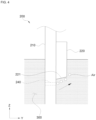
- FIG. 3 illustrates a partially enlarged cross-sectional view of the PCB module 200 of the electrical device according to a first embodiment of the present invention.
- a first component group 220 may be mounted on the first bonding portion 225 formed on one surface of the PCB 210, and a second component 230 may be mounted on the second bonding portion 235 formed on the other surface of the PCB 210.
- the through hole 400 may be formed by being spaced apart by a predetermined distance from the lower end of the first component 220 to the lower side.
- the filler 300 may be formed to be in contact with one surface and the other surface of the PCB 210 at a predetermined height.
- a height of the first component 220 in the vertical direction of the PCB surface is H1
- a separation distance of the first component 220 from the through hole 400 in the length direction is D1
- a height of the second component 230 in the vertical direction of the PCB surface is H2
- a separation distance of the second component 230 from the through hole 400 in the length direction is D2
- H1 of the first component 220 is equal to or greater than H2 of the second component 230
- D1 of the first component 220 may be configured to be shorter than D2 of the second component 230.
- the air pockets generated at the lower end of the first component 220 on one side of the PCB 210 may be configured to be more easily discharged to the other side of the PCB 210 through the through hole 400 by disposing through hole 400 to be close to the first component having the high component height.
- FIG. 4 illustrates a partially enlarged cross-sectional view of the PCB module 200 according to a second embodiment of the present invention.
- the first component 220 may be mounted on one surface of the PCB 210, and the through hole 400 may be formed by being spaced apart by a predetermined distance from the lower end of the first component 220 to the lower side.
- the filler 300 may be formed to be in contact with one surface and the other surface of the PCB 210 at a predetermined height.
- the first component 220 may be formed to be inclined upward as a lower surface 221 thereof is further away from the PCB 210 in the thickness direction. Therefore, the air pockets (Air) may be easily discharged by allowing the air pockets (Air) generated at the lower side of the first component 220 to be guided upward along the lower surface 221 of the first component 220. In addition, the air pockets may be easily discharged by allowing the air pockets (Air) flowing from the other surface of the PCB 210 to one surface thereof through the through hole 400 to be also guided upward along the lower surface 221 of the first component 220.
- the lower surface 221 of the first component 220 may be formed in any shape as long as it is not a shape in which the air pockets may be stagnated, for example, a shape that is concave inward in the length direction. That is, the lower surface 221 of the first component 220 may be formed of a curved surface that is convex outward in a plane or in a length direction. In addition, the inclination of the lower surface 221 may also be made at any angle as long as it is an angle that may guide the air pockets upward.
- FIG. 5 illustrates a partially enlarged cross-sectional view of the PCB module 200 according to a third embodiment of the present invention.
- the first component 220 may be mounted on one surface of the PCB 210, and the through hole 400 may be formed by being spaced apart by a predetermined distance from the lower end of the first component 220 to the lower side.
- the filler 300 may be formed to be in contact with one surface and the other surface of the PCB 210 at a predetermined height.
- the PCB module 200 may be configured as follows.
- the PCB module 200 may be provided with an air pocket prevention reinforcing agent 260 between the lower surface of the first component 220 and the upper end of the through hole 400.
- the reinforcing agent 260 has the other end in the thickness direction connected to the PCB 210, and one end in the thickness direction connected to the lowermost end on the lower surface of the first component 220 or the outermost in the thickness direction on the lower surface, and may be formed to be inclined upward as it is further away from the PCB 210 in the thickness direction.
- the air pockets may be easily discharged by allowing the air pockets (Air) generated at the lower side of the first component 220 to be guided upward along the reinforcing agent 260.
- the air pockets may be easily discharged by allowing the air pockets flowing from the other surface of the PCB 210 to one surface thereof through the through hole 400 to be also guided upward along the reinforcing agent 260.
- the reinforcing agent 260 may be formed in any shape as long as it is not a shape in which the air pockets may be stagnated, for example, a shape that is concave inward in the length direction. That is, the lower surface 221 of the first component 220 may be formed of a curved surface that is convex outward in a plane or in a length direction.
- the inclination of the reinforcing agent 260 may also be made at any angle as long as it is an angle that may guide the air pockets upward.
- the reinforcing agent 260 may be made of a material such as resin, polycarbonate (PC), or lead.
- FIG. 6 illustrates a partially enlarged cross-sectional view of the PCB module 200 according to a fourth embodiment of the present invention.
- the first component 220 may be mounted on the first bonding portion 225 formed on one surface of the PCB 210, and the through hole 400 may be formed from the lower end of the first component 220 to the lower side.
- the filler 300 may be formed to be in contact with one surface and the other surface of the PCB 210 at a predetermined height.
- the lowermost end 410 may be formed to be lower than the lowermost end of the first component 220, and the uppermost end 420 may be formed to be higher than the lowermost end of the first component 220. That is, the through hole 400 may be formed such that the lower end portion of the first component 220 is exposed along a penetration direction of the through hole 400.
- a distance D4 between the upper end of the through hole 400 and a specific height of the lower end of the PCB 210 may be longer than a distance D3 between the lower end of the first component 220 and the specific height of the lower end of the PCB 210.
- the PCB module 200 is configured to prevent the air pockets generated at the lower side of the first component 220 from being not discharged through the through hole 400 and from being stagnated between the lower side of the first component 220 and the through hole 400.
- FIG. 7 illustrates a partially enlarged cross-sectional view of the PCB module 200 according to a fifth embodiment of the present invention.
- a third component 240 is mounted on one surface of the PCB 210, and includes first and second leg portions 241 and 242 soldered to the PCB 210 so that they are disposed to be spaced apart from each other in one side in the thickness direction on one surface of the PCB 210, and connecting the PCB 210 and the third component 240.
- the first and second leg portions 241 and 242 are disposed to be vertically spaced apart from each other, and may include a first leg portion 241 positioned at a lower side and a second leg portion 242 positioned at an upper side.
- the through hole 400 may be formed in the PCB 210 adjacent to the third component 240, and the filler 300 may be formed to be in contact with one surface and the other surface of the PCB 210 at a predetermined height.
- the through hole 400 has the following characteristic configuration to prevent stagnation of the air pockets generated on a component separation space 243 between the first leg portion 241 and the second leg portion 242. That is, an upper end of the through hole 400 may be formed to be equal to or higher than a lower end of the second leg portion 242, and a lower end thereof may be formed to be equal to or higher than an upper end of the first leg portion 241.
- a distance D6 between the upper end of the through hole 400 and a specific height of the lower end of the PCB 210 may be longer than a distance D5 between the lower end of the second leg portion 242 and the specific height of the lower end of the PCB 210.
- the PCB module 200 is configured so that the air pockets generated on the component separation space 243 may be smoothly discharged to the other surface of the PCB 210 through the through hole 400.
- FIG. 8 illustrates a partially enlarged cross-sectional view of the PCB module 200 according to a sixth embodiment of the present invention.
- the first component 220 and a fourth component 250 may be mounted on one surface of the PCB 210, and the fourth component 250 may be formed on an upper side of the first component 220 to be spaced apart.
- the through hole 400 may be formed from the lower end of the first component 220 to the lower side, and the filler 300 may be formed to be in contact with one surface and the other surface of the PCB 210 at a predetermined height. At this time, the filler 300 is formed to be in contact with at least a partial region of the first component 220 and to be in non-contact with the fourth component 250. At this time, the amount of heat generation of the first component 220 is greater than that of the fourth component 250.
- the first component 220 may include, for example, a transformer or a semiconductor switch, and the fourth component 250 may include a capacitor.
- a maximum allowable temperature of the fourth component 250 may be configured to be higher than a maximum allowable temperature of the first component 220. Therefore, the fourth component 250 is configured to ensure durability during heat generation even if heat is not radiated through the filler 300.
- the weight of the heaviest component among the first components 220 may be heavier than the weight of the heaviest component among the fourth components 250. This is to make the weight of the lower side of the case 100 relatively heavier than the upper side of the case 100 so as to impact the ground from the lower side of the electrical device having relatively high strength during a drop test.
- FIG. 9 illustrates a side view of the PCB 210 in which through holes 400 are formed according to various embodiments of the present invention.
- the through holes formed to penetrate through the PCB 210 may be through holes 401, 402, 403, and 404 in the form of a hole forming a closed curve, and may also be through holes 405, 406, and 407 in a form of a slit that is partially opened.
- the shape of the through hole 400 may be a circular through hole 401, a polygonal through hole 402, or elliptical through holes 403 and 404.
- the through hole 400 may also be used for at least one of insertion, fixing, and reverse insertion prevention of components such as an insulating member, a connector pin, and a transformer. More specifically, the through hole 400 may be a hole for fixing a position of a bobbin of a transformer or a line filter on the PCB or preventing reverse insertion when assembling to the PCB.
- the through hole 400 may simultaneously include a region including a (metallic) soldering portion around a periphery to solder the component to the PCB, and a region that does not include the (metallic) soldering portion around the periphery so that the resin material or air contained in the resin material may pass through.
- a portion of one through hole may be soldered with a leg of the component penetrating through the PCB, and the other portion of the through hole may maintain a region that is not soldered and penetrated so that the resin material or air can pass through.
- the through hole may include a partition portion in which a cross-sectional area between the region for soldering and the resin material or air passage region is relatively narrowed.
- the through hole is in the shape of a gourd bottle, and a center thereof is slim, the top and bottom thereof are convex, an upper portion thereof is soldered with the leg of the component that penetrates including a metal foil around the periphery, and a lower portion thereof does not contain the metal foil around the periphery, such that the lower portion may not be soldered when soldering the component to the PCB.
- the component is coupled to the PCB through the upper region of the through hole and air, which may be located at the lower end of the component, passes through the lower region of the through hole toward a surface opposite to the surface of the PCB to which the component is coupled, thereby making it possible to suppress the air-pockets.
- the degree of integration may be increased by using the PCB more efficiently.
- the through hole is in the shape of a gourd bottle, and a center thereof is slim, the left and right thereof are convex, one side the left and right thereof is soldered with the leg of the component that penetrates including a metal foil around the periphery, and the other side thereof does not contain the metal foil around the periphery, such that the other side may not be soldered when soldering the component to the PCB.
- an air pocket suppression effect may be lower than that of the vertical gourd bottle-shaped through hole, the horizontal gourd bottle-shaped through hole may be formed when the vertical gourd bottle-shaped through hole may not be provided due to certain constraints such as component placement.
- the horizontal gourd bottle-shaped through hole may be provided at an angle inclined to the ground at a predetermined angle.
- a portion of the through hole 400 accommodates the leg of the component to prevent the reverse insertion of the component into the PCB or fix the component to the PCB
- the other portion of the through hole may be a region through which the resin material or air may pass.
- the through hole may include a partition portion in which a cross-sectional area between the region for accommodating the leg of the component and the resin material or air passage region is relatively narrowed.
- the vertical, horizontal, or diagonal gourd bottle-shaped through hole may not include the metal foil around the periphery.
- the air pockets may be prevented by changing only the shape of the through hole for inserting the component, fixing the component, and preventing the reverse insertion without additionally configuring a separate air pocket prevention through hole, the degree of integration may be increased by using the PCB more efficiently.
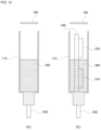
- FIG. 10 is a schematic cross-sectional view illustrating a manufacturing method of an electrical device according to the first embodiment of the present invention, where the manufacturing method itself is not a claimed embodiment.
- a step of forming the filler 300 by injecting a resin material into the body 110 of the case 100 having an opened upper side and forming an internal space is performed.
- a step of accommodating the PCB module 200 in the body 110 on which the filler 300 is formed is performed.
- the PCB module 200 is divided into a first region in contact with the filler 300 and a region in which the filler 300 does not contact.
- the lower end of the PCB module 200 may be electrically connected to the terminal pin 500.
- vibration is applied to the case 100 to more smoothly discharge the air pockets included in the filler 300 to the outside, and to improve fluidity of the resin material to be filled in the body 110.
- the case 100 when or after accommodating the PCB module 200, the case 100 may be tilted to more smoothly discharge the air pockets included in the filler 300 to the outside, and to improve fluidity of the resin material to be filled in the body 110. More preferably, by repeatedly tilting the case in one direction and the other direction for a predetermined number of times, the air pockets may be more smoothly discharged to the outside.
- the resin material is cured by maintaining the case 100 filled with the resin material at a predetermined temperature or higher.
- the predetermined temperature may be room temperature, preferably 50 to 200 degrees Celsius.
- cover 150 is coupled to the upper opening portion of the body 110 to seal the internal space of the body 110.
- FIG. 11 is a schematic cross-sectional view illustrating a manufacturing method of an electrical device according to the second embodiment of the present invention, where the manufacturing method itself is not a claimed embodiment.
- vibration is applied to the case 100 to more smoothly discharge the air pockets included in the filler 300 to the outside, and to improve fluidity of the resin material to be filled in the body 110.
- the case 100 when or after injecting the resin material, the case 100 may be tilted to more smoothly discharge the air pockets included in the filler 300 to the outside, and to improve fluidity of the resin material to be filled in the body 110. More preferably, by repeatedly tilting the case in one direction and the other direction for a predetermined number of times, the air pockets may be more smoothly discharged to the outside.
- the resin material is cured by maintaining the case 100 filled with the resin material at a predetermined temperature or higher.
- the predetermined temperature may be room temperature.
- cover 150 is coupled to the upper opening portion of the body 110 to seal the internal space of the body 110.
- the air-pocket prevention PCB, the air-pocket prevention module, the electrical device including the same, and the manufacturing method of the electrical device including the same according to the present invention having the configurations as described above may prevent the air pockets from being formed in the filler, thereby improving the fixing force and heat dissipation performance of the PCB module through the resin material.
Landscapes
- Engineering & Computer Science (AREA)
- Microelectronics & Electronic Packaging (AREA)
- Physics & Mathematics (AREA)
- Thermal Sciences (AREA)
- Manufacturing & Machinery (AREA)
- Casings For Electric Apparatus (AREA)
- Cooling Or The Like Of Electrical Apparatus (AREA)
- Structures For Mounting Electric Components On Printed Circuit Boards (AREA)
- Separation By Low-Temperature Treatments (AREA)
- Shielding Devices Or Components To Electric Or Magnetic Fields (AREA)
- Control Of Electric Motors In General (AREA)
Claims (11)
- Elektrische Vorrichtung (1000), umfassend:ein Gehäuse (100) mit einem Innenraum, einem Füllmittel (300), das in mindestens einen Abschnitt des Innenraums gefüllt ist und aus einem Harzmaterial gebildet ist, einer Leiterplatte (210), die in dem Innenraum untergebracht ist, und wobei der mindestens eine Abschnitt des Innenraums einen ersten Bereich definiert, der in das Füllmittel (300) eingetaucht ist, wobei der Innenraum ferner einen zweiten Bereich definiert, der sich von dem ersten Bereich unterscheidet, wobei der zweite Bereich nicht in das Füllmittel (300) eingetaucht ist,wobei:ein Ende und ein anderes Ende der Leiterplatte (210) einander gegenüberliegend positioniert sind, wobei die Leiterplatte (210) eine erste Oberfläche und eine zweite Oberfläche gegenüber der ersten Oberfläche umfasst, wobei sich die erste Oberfläche und die zweite Oberfläche zwischen dem einen Ende und dem anderen Ende erstrecken,die Leiterplatte (210) einen ersten Abschnitt und einen zweiten Abschnitt umfasst,das andere Ende der Leiterplatte (210) in das Harzmaterial eingetaucht ist,der erste Abschnitt der Leiterplatte (210) an einer Position bereitgestellt ist, die in das Harzmaterial eingetaucht ist, sodass ein Abschnitt der ersten Oberfläche und ein entsprechender, gegenüberliegender Abschnitt der zweiten Oberfläche an dem ersten Bereich zwischen einer Oberseite des Füllmittels (300) und dem anderen Ende der Leiterplatte (210) bereitgestellt sind,der zweite Abschnitt der Leiterplatte (210) das eine Ende der Leiterplatte umfasst und nicht von dem Harzmaterial bedeckt ist, sodass ein Abschnitt der ersten Oberfläche und ein entsprechender, gegenüberliegender Abschnitt der zweiten Oberfläche an dem zweiten Bereich zwischen dem einen Ende der Leiterplatte (210) und der Oberseite des Füllmittels (300) bereitgestellt sind,die Leiterplatte (200) einen Lötverbindungsabschnitt (225, 235) zum Schweißen-Löten einer Komponente (220, 230, 240, 250) umfasst;wobei die elektrische Vorrichtung ferner umfasst:eine Vielzahl von Komponenten (220, 230, 240, 250), die auf dem Lötverbindungsabschnitt (225, 235) montiert sind, wobei die Vielzahl von Komponenten eine erste Komponente (220) und eine zweite Komponente (230, 240, 250) beinhaltet, wobei mindestens die erste Komponente (220) in den ersten Bereich des Innenraums eingetaucht oder teilweise eingetaucht ist;dadurch gekennzeichnet, dass die elektrische Vorrichtung (1000) ferner umfasst:ein Durchgangsloch (400), das von einem Umfang der Leiterplatte (210) beabstandet ist und die Leiterplatte (210) durchdringt,wobei das Durchgangsloch (400) auf dem ersten Bereich bereitgestellt ist, sodass während des Füllens des Harzmaterials eine Lufttasche, die in dem Harzmaterial enthalten ist, die erste Oberfläche und die zweite Oberfläche der Leiterplatte durchdringen kann, um an die Oberseite des Füllmittels abgegeben zu werden.
- Elektrische Vorrichtung (1000) nach Anspruch 1, wobei die zweite Komponente (250) auf dem zweiten Bereich des Innenraums angeordnet ist, und
die Wärmeerzeugungsmenge der ersten Komponente (220) größer als die Wärmeerzeugungsmenge der zweiten Komponente (250) ist. - Elektrische Vorrichtung (1000) nach Anspruch 1 oder 2, wobei das Durchgangsloch (400) zwischen der ersten Komponente (220) und dem anderen Ende der Leiterplatte (210) angeordnet ist.
- Elektrische Vorrichtung (1000) nach einem der Ansprüche 1 bis 3, wobei ein Abschnitt der ersten Komponente (220) das Durchgangsloch (400) überlappt.
- Elektrische Vorrichtung (1000) nach einem von Anspruch 1 oder Anspruch 3, wenn abhängig von Anspruch 1, wobeidie erste Komponente (220) auf der ersten Oberfläche der Leiterplatte (210) an dem ersten Bereich angeordnet ist, die zweite Komponente (230) auf der zweiten Oberfläche der Leiterplatte (210) an dem ersten Bereich angeordnet ist,die erste und die zweite Komponente (220, 230) jeweils auf einer Seite des Durchgangslochs (400) angeordnet sind,eine erste Höhe der ersten Komponente (220) gleich oder größer als eine zweite Höhe der zweiten Komponente (230) ist, unddie erste Komponente (220) näher an dem Durchgangsloch (400) als die zweite Komponente (230) angeordnet ist.
- Elektrische Vorrichtung (1000) nach einem von Anspruch 1 oder Anspruch 3, wenn abhängig von Anspruch 1, wobei die erste Komponente (220) auf einer Seite des Durchgangslochs (400) angeordnet ist,die erste Komponente (220) eine Seitenfläche aufweist, die die erste Oberfläche der Leiterplatte (210), auf der die erste Komponente (220) montiert ist, schneidet und an das Durchgangsloch (400) angrenzt, unddie Seitenfläche der ersten Komponente (220) einen stumpfen Winkel in Bezug auf einen Abschnitt der ersten Oberfläche der Leiterplatte (210) aufweist, der zwischen der Seitenfläche der ersten Komponente (220) und dem Durchgangsloch (400) angeordnet ist.
- Elektrische Vorrichtung (1000) nach einem von Anspruch 1 oder Anspruch 3, wenn abhängig von Anspruch 1, wobei die erste Komponente (220) auf einer Seite des Durchgangslochs (400) angeordnet ist,die erste Komponente (220) eine Seitenfläche aufweist, die die erste Oberfläche der Leiterplatte (210), auf der die erste Komponente (220) montiert ist, schneidet und an das Durchgangsloch (400) angrenzt,die elektrische Vorrichtung (1000) ferner ein Verstärkungsmittel (260) auf der Seitenfläche umfasst, undeine Oberfläche des Verstärkungsmittels (260) einen stumpfen Winkel in Bezug auf einen Abschnitt der ersten Oberfläche der Leiterplatte (210) aufweist, der zwischen dem Verstärkungsmittel (260) und dem Durchgangsloch (400) angeordnet ist.
- Elektrische Vorrichtung (1000) nach einem der Ansprüche 1 bis 4, wobei die erste Komponente (220) umfasst:einen Körperabschnitt, der auf der Leiterplatte (210) angeordnet ist; undeinen ersten Schenkelabschnitt (241) und einen zweiten Schenkelabschnitt (242), die zwischen dem Körperabschnitt und der Leiterplatte (210) angeordnet und voneinander beabstandet sind,wobei:ein Abschnitt des ersten Schenkelabschnitts (241) das Durchgangsloch (400) überlappt, undder zweite Schenkelabschnitt (242) zwischen dem Durchgangsloch (400) und dem anderen Ende der Leiterplatte (210) angeordnet ist.
- Elektrische Vorrichtung (1000) nach einem der vorhergehenden Ansprüche, wobei die erste Komponente (220) mindestens eines von einem Transformator, einer Spule, einer Sicherung, einem Varistor und einem Kondensator umfasst.
- Elektrische Vorrichtung (1000) nach einem der vorhergehenden Ansprüche, wobei die maximal zulässige Temperatur der Komponenten, die in dem ersten Bereich bereitgestellt sind, niedriger ist als die maximal zulässige Temperatur einer der Komponenten, die in dem zweiten Bereich bereitgestellt sind.
- Elektrische Vorrichtung (1000) nach einem der vorhergehenden Ansprüche, wobei das Gewicht der schwersten Komponente unter den Komponenten, die in dem ersten Bereich bereitgestellt sind, schwerer ist als das Gewicht der schwersten Komponente unter den Komponenten, die in dem zweiten Bereich bereitgestellt sind.
Applications Claiming Priority (1)
| Application Number | Priority Date | Filing Date | Title |
|---|---|---|---|
| KR1020200171228A KR20230023834A (ko) | 2020-12-09 | 2020-12-09 | 에어포켓 방지 기판, 에어포켓 방지 기판 모듈, 이를 포함하는 전기기기 및 이를 포함하는 전기기기의 제조 방법 |
Publications (3)
| Publication Number | Publication Date |
|---|---|
| EP4013199A1 EP4013199A1 (de) | 2022-06-15 |
| EP4013199B1 true EP4013199B1 (de) | 2025-01-29 |
| EP4013199C0 EP4013199C0 (de) | 2025-01-29 |
Family
ID=78822093
Family Applications (1)
| Application Number | Title | Priority Date | Filing Date |
|---|---|---|---|
| EP21212431.7A Active EP4013199B1 (de) | 2020-12-09 | 2021-12-06 | Platine zur vermeidung von lufttaschen, modul zur verhinderung von lufttaschen, elektrische vorrichtung damit und herstellungsverfahren für eine elektrische vorrichtung damit |
Country Status (4)
| Country | Link |
|---|---|
| US (1) | US11825599B2 (de) |
| EP (1) | EP4013199B1 (de) |
| KR (2) | KR20230023834A (de) |
| CN (1) | CN114615793A (de) |
Family Cites Families (45)
| Publication number | Priority date | Publication date | Assignee | Title |
|---|---|---|---|---|
| US4143456A (en) * | 1976-06-28 | 1979-03-13 | Citizen Watch Commpany Ltd. | Semiconductor device insulation method |
| CH660551GA3 (de) * | 1982-12-27 | 1987-05-15 | ||
| JP3541491B2 (ja) * | 1994-06-22 | 2004-07-14 | セイコーエプソン株式会社 | 電子部品 |
| JP3127195B2 (ja) * | 1994-12-06 | 2001-01-22 | シャープ株式会社 | 発光デバイスおよびその製造方法 |
| US5832600A (en) * | 1995-06-06 | 1998-11-10 | Seiko Epson Corporation | Method of mounting electronic parts |
| EP0788127B1 (de) * | 1995-07-18 | 2004-05-06 | Omron Corporation | Elektronisches gerät und verfahren zu seiner herstellung |
| JP2000048693A (ja) * | 1998-07-30 | 2000-02-18 | Yamatake Corp | 近接スイッチ |
| EP1094087B1 (de) * | 1999-03-11 | 2004-09-08 | Toray Industries, Inc. | Expoxidharzzusammensetzung, expoxidharzzusammensetzung für faserverstärkte verbundwerkstoffe und diese enthaltende faserverstärkte verbundstoffe |
| JP2000307277A (ja) * | 1999-04-26 | 2000-11-02 | Matsushita Refrig Co Ltd | パワー制御装置 |
| JP4018375B2 (ja) * | 2000-11-30 | 2007-12-05 | 株式会社東芝 | 半導体装置 |
| DE50011223D1 (de) * | 2000-12-14 | 2005-10-27 | Hannecard Gmbh Pfaeffikon | Verfahren zum Austauschen des Mantels einer Walze zum Führen |
| JP2002203425A (ja) | 2000-12-28 | 2002-07-19 | Matsushita Electric Works Ltd | 放電灯点灯装置 |
| JP4016266B2 (ja) * | 2002-10-30 | 2007-12-05 | オムロン株式会社 | 近接センサの封止方法 |
| JP3900093B2 (ja) * | 2003-03-11 | 2007-04-04 | 日立電線株式会社 | モールド金型及びそれを用いた半導体装置の製造方法 |
| JP4146286B2 (ja) * | 2003-05-30 | 2008-09-10 | 株式会社ケーヒン | 電子回路基板の収容ケース |
| KR100517075B1 (ko) * | 2003-08-11 | 2005-09-26 | 삼성전자주식회사 | 반도체 소자 제조 방법 |
| JP2005240092A (ja) * | 2004-02-26 | 2005-09-08 | Dowa Mining Co Ltd | 銀粉およびその製造方法 |
| JP4430062B2 (ja) * | 2006-12-06 | 2010-03-10 | シャープ株式会社 | Icチップ実装パッケージの製造方法 |
| JP4219953B2 (ja) * | 2006-12-11 | 2009-02-04 | シャープ株式会社 | Icチップ実装パッケージ、およびその製造方法 |
| JP2008166331A (ja) * | 2006-12-27 | 2008-07-17 | Lecip Corp | 電子機器装置及びその電子機器装置の製造方法 |
| JP4858186B2 (ja) * | 2007-01-24 | 2012-01-18 | 住友電装株式会社 | 基板用コネクタ及びその組付方法 |
| KR20090023886A (ko) * | 2007-09-03 | 2009-03-06 | 삼성전자주식회사 | 전기전자제품 및 그 제조방법 |
| JP2009071110A (ja) | 2007-09-14 | 2009-04-02 | Toshiba Lighting & Technology Corp | 電気機器 |
| JP5353153B2 (ja) * | 2007-11-09 | 2013-11-27 | パナソニック株式会社 | 実装構造体 |
| JP2010010269A (ja) * | 2008-06-25 | 2010-01-14 | Elpida Memory Inc | 半導体装置、半導体装置製造用中間体およびそれらの製造方法 |
| JP2010153355A (ja) * | 2008-11-26 | 2010-07-08 | Toshiba Lighting & Technology Corp | 電気機器および照明装置 |
| DE102009029260A1 (de) | 2009-09-08 | 2011-03-10 | Robert Bosch Gmbh | Elektronikeinheit und Verfahren zum Herstellen derselben |
| JP2011150416A (ja) * | 2010-01-19 | 2011-08-04 | Toshiba Corp | 半導体メモリ装置 |
| JP2011249582A (ja) * | 2010-05-27 | 2011-12-08 | Elpida Memory Inc | 半導体装置 |
| JP5563918B2 (ja) * | 2010-07-22 | 2014-07-30 | セミコンダクター・コンポーネンツ・インダストリーズ・リミテッド・ライアビリティ・カンパニー | 回路装置の製造方法 |
| US9059187B2 (en) * | 2010-09-30 | 2015-06-16 | Ibiden Co., Ltd. | Electronic component having encapsulated wiring board and method for manufacturing the same |
| JP5699006B2 (ja) * | 2011-03-01 | 2015-04-08 | 日立オートモティブシステムズ株式会社 | 変速機制御装置及び電子回路装置 |
| US20130323536A1 (en) * | 2012-05-31 | 2013-12-05 | Samsung Sdi Co., Ltd. | Rechargeable battery pack |
| JP2014103183A (ja) * | 2012-11-19 | 2014-06-05 | Mitsubishi Electric Corp | 電子回路、その製造方法、および電子部品 |
| CN104604346B (zh) | 2013-08-30 | 2016-04-20 | 新电元工业株式会社 | 电气设备及其制造方法、以及电气设备的设计方法 |
| JP6016965B2 (ja) * | 2015-03-02 | 2016-10-26 | 三菱電機株式会社 | 電子機器ユニット及びその製造金型装置 |
| CN107615497B (zh) * | 2015-05-29 | 2019-05-21 | 西铁城电子株式会社 | 发光装置及其制造方法 |
| WO2016194405A1 (ja) * | 2015-05-29 | 2016-12-08 | シチズン電子株式会社 | 発光装置およびその製造方法 |
| DE202015104630U1 (de) | 2015-09-01 | 2016-12-02 | Tridonic Gmbh & Co Kg | Abdichtung von Leiterplattengehäusen |
| WO2018134933A1 (ja) * | 2017-01-19 | 2018-07-26 | オリンパス株式会社 | 光モジュールおよび内視鏡 |
| JP6642484B2 (ja) * | 2017-02-28 | 2020-02-05 | 株式会社デンソー | 半導体装置およびその製造方法 |
| JP7218126B2 (ja) * | 2018-08-30 | 2023-02-06 | キヤノン株式会社 | 配線板を備えるユニット、モジュールおよび機器 |
| JP2021036575A (ja) * | 2018-12-17 | 2021-03-04 | 東芝ホクト電子株式会社 | 発光装置、接合部の保護方法、発光装置の製造方法、及び、車両用灯具 |
| JP7362280B2 (ja) * | 2019-03-22 | 2023-10-17 | キヤノン株式会社 | パッケージユニットの製造方法、パッケージユニット、電子モジュール、および機器 |
| CN210897754U (zh) * | 2019-10-24 | 2020-06-30 | 丰田自动车株式会社 | 电力转换组件 |
-
2020
- 2020-12-09 KR KR1020200171228A patent/KR20230023834A/ko not_active Ceased
-
2021
- 2021-10-13 US US17/500,654 patent/US11825599B2/en active Active
- 2021-12-06 EP EP21212431.7A patent/EP4013199B1/de active Active
- 2021-12-08 CN CN202111490842.6A patent/CN114615793A/zh active Pending
-
2022
- 2022-09-07 KR KR1020220113560A patent/KR102574398B1/ko active Active
Also Published As
| Publication number | Publication date |
|---|---|
| CN114615793A (zh) | 2022-06-10 |
| US11825599B2 (en) | 2023-11-21 |
| US20220183145A1 (en) | 2022-06-09 |
| KR20230023834A (ko) | 2023-02-20 |
| EP4013199A1 (de) | 2022-06-15 |
| KR102574398B1 (ko) | 2023-09-06 |
| KR20220127217A (ko) | 2022-09-19 |
| EP4013199C0 (de) | 2025-01-29 |
Similar Documents
| Publication | Publication Date | Title |
|---|---|---|
| EP1826839B1 (de) | Sekundärbatterie | |
| US7754378B2 (en) | Secondary battery with a sealing plate used to seal an electrolyte injection hole in a cap plate | |
| CN1214482C (zh) | 蓄电池体 | |
| KR100965711B1 (ko) | 배터리 팩 | |
| US8923010B2 (en) | Electronic component for surface mounting | |
| CN101237031B (zh) | 二次电池的壳体和包括所述二次电池的壳体的电池封装体 | |
| CN115513561B (zh) | 电池包、充电系统及用电设备 | |
| CN104170117B (zh) | 具有新颖结构的二次电池组 | |
| JP6175218B2 (ja) | 二次電池 | |
| CN100583533C (zh) | 二次电池 | |
| CN106257652A (zh) | 封装模块 | |
| KR101234240B1 (ko) | 코어팩과 보호회로모듈 사이의 격벽을 포함하는 배터리 팩 | |
| CN116315415A (zh) | 电池模组以及电池包 | |
| CN110073515A (zh) | 防水构造的电池系统 | |
| US11825599B2 (en) | Air-pocket prevention PCB, air-pocket prevention PCB module, electrical device including the same, and manufacturing method of electrical device including the same | |
| US6191955B1 (en) | Encapsulation and enclosure of electronic modules | |
| KR20130051399A (ko) | 배터리 팩 | |
| KR101502900B1 (ko) | 전지 팩 | |
| KR101787069B1 (ko) | 배터리모듈용 직렬연결장치 | |
| CN224123427U (zh) | 一种工具电池包 | |
| CN116685055B (zh) | 电路板组件和电子设备 | |
| US12525674B1 (en) | Tool battery pack | |
| KR101735408B1 (ko) | 배터리팩 | |
| CN213244569U (zh) | 一种电机控制器的mos管安装结构及灌封夹具 | |
| CN110114868B (zh) | 嵌入式保护电路模块 |
Legal Events
| Date | Code | Title | Description |
|---|---|---|---|
| PUAI | Public reference made under article 153(3) epc to a published international application that has entered the european phase |
Free format text: ORIGINAL CODE: 0009012 |
|
| STAA | Information on the status of an ep patent application or granted ep patent |
Free format text: STATUS: THE APPLICATION HAS BEEN PUBLISHED |
|
| AK | Designated contracting states |
Kind code of ref document: A1 Designated state(s): AL AT BE BG CH CY CZ DE DK EE ES FI FR GB GR HR HU IE IS IT LI LT LU LV MC MK MT NL NO PL PT RO RS SE SI SK SM TR |
|
| STAA | Information on the status of an ep patent application or granted ep patent |
Free format text: STATUS: REQUEST FOR EXAMINATION WAS MADE |
|
| 17P | Request for examination filed |
Effective date: 20221215 |
|
| RBV | Designated contracting states (corrected) |
Designated state(s): AL AT BE BG CH CY CZ DE DK EE ES FI FR GB GR HR HU IE IS IT LI LT LU LV MC MK MT NL NO PL PT RO RS SE SI SK SM TR |
|
| STAA | Information on the status of an ep patent application or granted ep patent |
Free format text: STATUS: EXAMINATION IS IN PROGRESS |
|
| 17Q | First examination report despatched |
Effective date: 20240229 |
|
| GRAP | Despatch of communication of intention to grant a patent |
Free format text: ORIGINAL CODE: EPIDOSNIGR1 |
|
| STAA | Information on the status of an ep patent application or granted ep patent |
Free format text: STATUS: GRANT OF PATENT IS INTENDED |
|
| INTG | Intention to grant announced |
Effective date: 20240718 |
|
| GRAS | Grant fee paid |
Free format text: ORIGINAL CODE: EPIDOSNIGR3 |
|
| GRAA | (expected) grant |
Free format text: ORIGINAL CODE: 0009210 |
|
| STAA | Information on the status of an ep patent application or granted ep patent |
Free format text: STATUS: THE PATENT HAS BEEN GRANTED |
|
| AK | Designated contracting states |
Kind code of ref document: B1 Designated state(s): AL AT BE BG CH CY CZ DE DK EE ES FI FR GB GR HR HU IE IS IT LI LT LU LV MC MK MT NL NO PL PT RO RS SE SI SK SM TR |
|
| REG | Reference to a national code |
Ref country code: GB Ref legal event code: FG4D |
|
| REG | Reference to a national code |
Ref country code: CH Ref legal event code: EP |
|
| REG | Reference to a national code |
Ref country code: DE Ref legal event code: R096 Ref document number: 602021025341 Country of ref document: DE |
|
| REG | Reference to a national code |
Ref country code: IE Ref legal event code: FG4D |
|
| U01 | Request for unitary effect filed |
Effective date: 20250129 |
|
| U07 | Unitary effect registered |
Designated state(s): AT BE BG DE DK EE FI FR IT LT LU LV MT NL PT RO SE SI Effective date: 20250204 |
|
| PG25 | Lapsed in a contracting state [announced via postgrant information from national office to epo] |
Ref country code: RS Free format text: LAPSE BECAUSE OF FAILURE TO SUBMIT A TRANSLATION OF THE DESCRIPTION OR TO PAY THE FEE WITHIN THE PRESCRIBED TIME-LIMIT Effective date: 20250429 |
|
| PG25 | Lapsed in a contracting state [announced via postgrant information from national office to epo] |
Ref country code: PL Free format text: LAPSE BECAUSE OF FAILURE TO SUBMIT A TRANSLATION OF THE DESCRIPTION OR TO PAY THE FEE WITHIN THE PRESCRIBED TIME-LIMIT Effective date: 20250129 |
|
| PG25 | Lapsed in a contracting state [announced via postgrant information from national office to epo] |
Ref country code: ES Free format text: LAPSE BECAUSE OF FAILURE TO SUBMIT A TRANSLATION OF THE DESCRIPTION OR TO PAY THE FEE WITHIN THE PRESCRIBED TIME-LIMIT Effective date: 20250129 |
|
| PG25 | Lapsed in a contracting state [announced via postgrant information from national office to epo] |
Ref country code: IS Free format text: LAPSE BECAUSE OF FAILURE TO SUBMIT A TRANSLATION OF THE DESCRIPTION OR TO PAY THE FEE WITHIN THE PRESCRIBED TIME-LIMIT Effective date: 20250529 Ref country code: NO Free format text: LAPSE BECAUSE OF FAILURE TO SUBMIT A TRANSLATION OF THE DESCRIPTION OR TO PAY THE FEE WITHIN THE PRESCRIBED TIME-LIMIT Effective date: 20250429 |
|
| PG25 | Lapsed in a contracting state [announced via postgrant information from national office to epo] |
Ref country code: HR Free format text: LAPSE BECAUSE OF FAILURE TO SUBMIT A TRANSLATION OF THE DESCRIPTION OR TO PAY THE FEE WITHIN THE PRESCRIBED TIME-LIMIT Effective date: 20250129 |
|
| PG25 | Lapsed in a contracting state [announced via postgrant information from national office to epo] |
Ref country code: GR Free format text: LAPSE BECAUSE OF FAILURE TO SUBMIT A TRANSLATION OF THE DESCRIPTION OR TO PAY THE FEE WITHIN THE PRESCRIBED TIME-LIMIT Effective date: 20250430 |
|
| PG25 | Lapsed in a contracting state [announced via postgrant information from national office to epo] |
Ref country code: SM Free format text: LAPSE BECAUSE OF FAILURE TO SUBMIT A TRANSLATION OF THE DESCRIPTION OR TO PAY THE FEE WITHIN THE PRESCRIBED TIME-LIMIT Effective date: 20250129 |
|
| PG25 | Lapsed in a contracting state [announced via postgrant information from national office to epo] |
Ref country code: CZ Free format text: LAPSE BECAUSE OF FAILURE TO SUBMIT A TRANSLATION OF THE DESCRIPTION OR TO PAY THE FEE WITHIN THE PRESCRIBED TIME-LIMIT Effective date: 20250129 |
|
| PG25 | Lapsed in a contracting state [announced via postgrant information from national office to epo] |
Ref country code: SK Free format text: LAPSE BECAUSE OF FAILURE TO SUBMIT A TRANSLATION OF THE DESCRIPTION OR TO PAY THE FEE WITHIN THE PRESCRIBED TIME-LIMIT Effective date: 20250129 |
|
| PLBE | No opposition filed within time limit |
Free format text: ORIGINAL CODE: 0009261 |
|
| STAA | Information on the status of an ep patent application or granted ep patent |
Free format text: STATUS: NO OPPOSITION FILED WITHIN TIME LIMIT |
|
| 26N | No opposition filed |
Effective date: 20251030 |
|
| U20 | Renewal fee for the european patent with unitary effect paid |
Year of fee payment: 5 Effective date: 20251223 |