EP4012735B1 - Verfahren zur herstellung eines kondensators - Google Patents
Verfahren zur herstellung eines kondensators Download PDFInfo
- Publication number
- EP4012735B1 EP4012735B1 EP21213288.0A EP21213288A EP4012735B1 EP 4012735 B1 EP4012735 B1 EP 4012735B1 EP 21213288 A EP21213288 A EP 21213288A EP 4012735 B1 EP4012735 B1 EP 4012735B1
- Authority
- EP
- European Patent Office
- Prior art keywords
- plasma etching
- etching
- chemical
- layer
- conductive layer
- Prior art date
- Legal status (The legal status is an assumption and is not a legal conclusion. Google has not performed a legal analysis and makes no representation as to the accuracy of the status listed.)
- Active
Links
Images


Classifications
-
- H—ELECTRICITY
- H01—ELECTRIC ELEMENTS
- H01G—CAPACITORS; CAPACITORS, RECTIFIERS, DETECTORS, SWITCHING DEVICES, LIGHT-SENSITIVE OR TEMPERATURE-SENSITIVE DEVICES OF THE ELECTROLYTIC TYPE
- H01G4/00—Fixed capacitors; Processes of their manufacture
- H01G4/33—Thin- or thick-film capacitors (thin- or thick-film circuits; capacitors without a potential-jump or surface barrier specially adapted for integrated circuits, details thereof, multistep manufacturing processes therefor)
-
- H—ELECTRICITY
- H10—SEMICONDUCTOR DEVICES; ELECTRIC SOLID-STATE DEVICES NOT OTHERWISE PROVIDED FOR
- H10D—INORGANIC ELECTRIC SEMICONDUCTOR DEVICES
- H10D1/00—Resistors, capacitors or inductors
- H10D1/01—Manufacture or treatment
- H10D1/041—Manufacture or treatment of capacitors having no potential barriers
- H10D1/043—Manufacture or treatment of capacitors having no potential barriers using patterning processes to form electrode extensions, e.g. etching
-
- H—ELECTRICITY
- H10—SEMICONDUCTOR DEVICES; ELECTRIC SOLID-STATE DEVICES NOT OTHERWISE PROVIDED FOR
- H10D—INORGANIC ELECTRIC SEMICONDUCTOR DEVICES
- H10D1/00—Resistors, capacitors or inductors
- H10D1/60—Capacitors
- H10D1/68—Capacitors having no potential barriers
- H10D1/692—Electrodes
- H10D1/711—Electrodes having non-planar surfaces, e.g. formed by texturisation
- H10D1/714—Electrodes having non-planar surfaces, e.g. formed by texturisation having horizontal extensions
-
- H—ELECTRICITY
- H10—SEMICONDUCTOR DEVICES; ELECTRIC SOLID-STATE DEVICES NOT OTHERWISE PROVIDED FOR
- H10D—INORGANIC ELECTRIC SEMICONDUCTOR DEVICES
- H10D1/00—Resistors, capacitors or inductors
- H10D1/60—Capacitors
- H10D1/68—Capacitors having no potential barriers
- H10D1/692—Electrodes
- H10D1/711—Electrodes having non-planar surfaces, e.g. formed by texturisation
- H10D1/716—Electrodes having non-planar surfaces, e.g. formed by texturisation having vertical extensions
-
- H—ELECTRICITY
- H10—SEMICONDUCTOR DEVICES; ELECTRIC SOLID-STATE DEVICES NOT OTHERWISE PROVIDED FOR
- H10D—INORGANIC ELECTRIC SEMICONDUCTOR DEVICES
- H10D1/00—Resistors, capacitors or inductors
- H10D1/60—Capacitors
- H10D1/68—Capacitors having no potential barriers
Definitions
- the document KR20030056917A describes an example of a known method of manufacturing a capacitor comprising two chemical etching steps.
- said chemical plasma etching in step b), comprises a first step of chemical plasma etching using a chlorine-based plasma, followed by a second step of chemical plasma etching using a fluorine-based plasma.
- the second chemical plasma etching step and the physical plasma etching step are implemented in the same etching chamber, a step of purging said etching chamber being implemented between the two steps.
- said chemical plasma etching in step b), comprises a single step of chemical plasma etching using a chlorine-based plasma.
- said chemical plasma etching in step b), comprises a single step of chemical plasma etching using a fluorine-based plasma.
- the stack further comprises a second conductive layer coating the second electrode.
- the physical plasma etching, in step c), is carried out using an argon plasma.
- the second conductive layer is made of aluminum or an alloy comprising aluminum.
- the first electrode is made of tantalum nitride.
- the expressions "about”, “approximately”, “substantially”, and “of the order of” mean to within 10%, preferably to within 5%.
- FIG. 1 is a sectional view of an example of a capacitor 11 according to one embodiment.
- the redistribution layer 13 is in contact, by its lower face, with the upper face of the substrate 21, the lower electrode 15 is in contact, by its lower face, with the upper face of the layer 13, the dielectric layer 17 is in contact, by its lower face, with the upper face of the lower electrode 15, and the upper electrode 19 is in contact, by its lower face, with the upper face of the dielectric layer 17.
- the conductive layer 13 is made of aluminum or an alloy comprising aluminum, for example an aluminum and copper alloy (AlCu) or an aluminum, copper and silicon alloy (AlSiCu).
- AlCu aluminum and copper alloy
- AlSiCu aluminum, copper and silicon alloy
- the layer 13 has a thickness of between 0.5 ⁇ m and 3 ⁇ m, preferably equal to approximately 1.5 ⁇ m.
- the metal pad 25 is, for example, made of copper.
- Layer 23 can then be etched by a first chemical plasma etching, for example using a chlorine-based plasma, opposite the opening formed in layer 29, using layer 29 as an etching mask.
- a first chemical plasma etching for example using a chlorine-based plasma
- layer 23 is etched over its entire thickness during this first chemical etching.
- the second chemical etching step has the advantage of etching layers 19, 17 and 15 selectively compared to layer 13, containing aluminum.
- a disadvantage of this method is that, during the second step of chemical plasma etching, the fluorine-based plasma comes into contact with the upper face of the conductive layer 13, containing aluminum. Fluorine atoms then bond with aluminum atoms on the surface of the layer 13, creating a monatomic layer 35 of aluminum fluoride (AlF) on the surface of the layer 13. As schematically illustrated in Figure 4 , the layer 35 is irregular and does not continuously cover the exposed portion of the conductive layer 13.
- FIG. 5 illustrates the structure obtained following a subsequent wet chemical etching step, for example using one or more acids, for example using a solution known under the trade name "Pvapox", comprising a mixture of hydrofluoric acid (HF), ammonium fluoride (NH 4 F), acetic acid (CH 3 COOH) and benzotriazole (C 6 H 5 N 3 ).
- Pvapox hydrofluoric acid
- NH 4 F ammonium fluoride
- CH 3 COOH acetic acid
- benzotriazole C 6 H 5 N 3
- This wet chemical etching can for example be used to locally remove, opposite the upper face of the conductive layer 13, a passivation layer (not visible in the figures) previously deposited on the upper face of the structure of the Figure 4 .
- the wet chemical etching is for example preceded by a step (not detailed in the figures) of depositing a layer of an oxide, for example a USG layer on the entire structure.
- the wet chemical etching step makes it possible in particular to remove a part of the oxide layer located on and in contact with the upper face of the portion of the layer 13 exposed to the plasma etching step of the Figure 4 .
- the etching solution used in the step of Figure 5 tends to superficially consume the exposed part of the conductive layer 13. However, this superficial etching is blocked by the residues 35 of aluminum fluoride, which are resistant to the solution used and more generally to acid attacks.
- a micro-masking phenomenon thus occurs, leading to the formation of roughness on the upper face of the conductive layer 13.
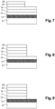
- THE figures 6 , 7, 8 and 9 are sectional views illustrating successive steps of an example of a method of manufacturing the capacitor 11 of the Figure 1 according to a first embodiment.
- FIG. 7 illustrates the structure obtained at the end of a step of localized removal of the protective layer 29 and the upper conductive layer 23 opposite the portion of the lower conductive layer 13 that it is desired to expose.
- the first chemical etching is interrupted on the upper face of the electrode 19.
- layers 19 and 17 are etched over their entire thickness during this second chemical etching.
- the second chemical plasma etching is interrupted before reaching the upper face of the lower conductive layer 13.
- the second chemical plasma etching is interrupted on the upper face of the lower electrode 15.
- the second chemical plasma etching is for example similar to what was described above in relation to the Figure 4 .
- the second chemical plasma etching is carried out using a fluorine-based plasma.
- FIG. 9 illustrates the structure obtained at the end of a step of localized removal of the lower electrode layer 15 opposite the portion of the lower conductive layer 13 that it is desired to expose.
- the layer 15 is removed by physical plasma etching, using a plasma of a gas having no affinity for aluminum, for example, a plasma of a neutral gas, for example an argon or nitrogen plasma, preferably an argon plasma.
- a plasma of a neutral gas for example an argon or nitrogen plasma, preferably an argon plasma.
- the physical etching is induced by ions of the neutral gas, for example argon ions, accelerated by a bias voltage.
- the physical etching speed of the electrode 15 is, for example, equal to approximately 50 nm/min whereas it is ten times greater during chemical plasma etching with fluorine and fifteen times greater during chemical plasma etching with chlorine.
- the physical plasma etching is interrupted when the upper face of the conductive layer 13 is revealed, that is to say when the electrode 15 has been etched over its entire thickness.
- An advantage of the method described in relation to the figures 6 to 9 is that we come to the conductive layer 13 using neutral physical plasma etching. This makes it possible to avoid the formation of aluminum fluoride on the exposed face of the conductive layer 13. Thus, the formation of roughness on the upper face of the conductive layer 13, as described in relation to the Figure 5 , can be avoided. This allows for a more reliable and efficient electrical connection to be made on the upper face of layer 13.
- the first chemical plasma etching ( Figure 7 ) may be continued through all or part of the thickness of the upper electrode 19 and be interrupted in the electrode 19 or on the upper face of the dielectric layer 17.
- the first chemical plasma etching can be continued through all or part of the thickness of the dielectric layer 17 and be interrupted in the dielectric layer 17 or on the upper face of the electrode 15.
- the second step of chemical plasma etching ( figure 8 ) is interrupted before reaching the upper face of the electrode 15, for example on the upper face of the dielectric layer 17 or in the dielectric layer 17.
- a portion of the thickness of the electrode 15 is removed during the second chemical plasma etching step.
- the second chemical plasma etching step is interrupted in the lower electrode layer 15.
- the first chemical plasma etching step is implemented in a first etching tool and the second chemical plasma etching step and the physical plasma etching step are implemented in a second etching tool different from the first tool.
- a purge of the etching chamber of the second tool can be carried out between the second chemical plasma etching step and the physical plasma etching step, so as to prevent fluorine atoms from remaining in the etching chamber during the physical plasma etching step.
- the purge has, for example, a duration of between 10 seconds and 20 seconds.
- the first step of chemical plasma etching by means of a chlorine-based plasma, can be omitted.
- only two etching steps can be provided, namely the second step of chemical plasma etching ( figure 8 ), using a fluorine-based plasma, and the physical plasma etching step ( Figure 9 ), by means of a plasma of a neutral gas, for example an argon plasma.
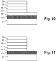
- FIGS. 10 and 11 are sectional views illustrating successive steps of an example of a method of manufacturing the capacitor 11 of the Figure 1 according to a second embodiment.
- the second step of chemical plasma etching, using a fluorine-based plasma is omitted.
- only two etching steps are provided, namely the first step of chemical plasma etching, using a chlorine-based plasma, and the step of physical plasma etching, using a plasma of a neutral gas, for example an argon plasma.
- the first chemical plasma etching is interrupted before reaching the upper face of the lower conductive layer 13.
Landscapes
- Engineering & Computer Science (AREA)
- Power Engineering (AREA)
- Microelectronics & Electronic Packaging (AREA)
- Manufacturing & Machinery (AREA)
- Semiconductor Integrated Circuits (AREA)
- Semiconductor Memories (AREA)
- Fixed Capacitors And Capacitor Manufacturing Machines (AREA)
Claims (10)
- Verfahren zur Herstellung eines Kondensators, das die folgenden aufeinanderfolgenden Schritte aufweist:a) Ausbilden eines Stapels aufweisend, in der Reihenfolge von der Oberseite eines Substrats (21) aus, eine erste leitfähige Schicht (13) aus Aluminium oder einer Aluminiumlegierung, eine erste Elektrode (15), eine erste dielektrische Schicht (17) und eine zweite Elektrode (19);b) Ätzen, durch chemisches Plasmaätzen, eines oberen Abschnitts des Stapels, wobei das chemische Plasmaätzen vor der Oberseite der ersten leitfähigen Schicht (13) unterbrochen wird; undc) Ätzen, durch physikalisches Plasmaätzen, eines unteren Abschnitts des Stapels wobei das physikalische Plasmaätzen auf der Oberseite der ersten leitfähigen Schicht (13) unterbrochen wird.
- Verfahren nach Anspruch 1, wobei in Schritt b) das chemische Plasmaätzen einen ersten Schritt des chemischen Plasmaätzens mittels eines chlorbasierten Plasmas, gefolgt von einem zweiten Schritt des chemischen Plasmaätzens mittels eines fluorbasierten Plasmas, aufweist.
- Verfahren nach Anspruch 2, wobei der zweite chemische Plasmaätzschritt und der physikalische Plasmaätzschritt in derselben Ätzkammer durchgeführt werden, wobei zwischen den beiden Schritten ein Spülschritt der Ätzkammer durchgeführt wird.
- Verfahren nach Anspruch 1, wobei in Schritt b) das chemische Plasmaätzen einen einzigen Schritt des chemischen Plasmaätzens mittels eines chlorbasierten Plasmas aufweist.
- Verfahren nach Anspruch 1, wobei in Schritt b) das chemische Plasmaätzen einen einzigen Schritt des chemischen Plasmaätzens mittels eines Fluor-basierten Plasmas aufweist.
- Verfahren nach einem der Ansprüche 1 bis 5, wobei der Stapel ferner eine zweite leitfähige Schicht (23) aufweist, die die zweite Elektrode (19) bedeckt.
- Verfahren nach einem der Ansprüche 1 bis 6, wobei in Schritt c) das physikalische Plasmaätzen mittels eines Argonplasmas durchgeführt wird.
- Verfahren nach einem der Ansprüche 1 bis 7, wobei die zweite leitfähige Schicht (23) aus Aluminium oder einer Aluminium enthaltenden Legierung besteht.
- Verfahren nach einem der Ansprüche 1 bis 8, wobei die erste Elektrode (15) aus Tantalnitrid besteht.
- Verfahren nach einem der Ansprüche 1 bis 9, wobei der untere Abschnitt des Stapels mindestens einen Teil der Dicke der ersten Elektrode (15) aufweist.
Applications Claiming Priority (1)
| Application Number | Priority Date | Filing Date | Title |
|---|---|---|---|
| FR2013214A FR3117663B1 (fr) | 2020-12-14 | 2020-12-14 | Procédé de fabrication d'un condensateur |
Publications (2)
| Publication Number | Publication Date |
|---|---|
| EP4012735A1 EP4012735A1 (de) | 2022-06-15 |
| EP4012735B1 true EP4012735B1 (de) | 2025-07-09 |
Family
ID=74592201
Family Applications (1)
| Application Number | Title | Priority Date | Filing Date |
|---|---|---|---|
| EP21213288.0A Active EP4012735B1 (de) | 2020-12-14 | 2021-12-09 | Verfahren zur herstellung eines kondensators |
Country Status (3)
| Country | Link |
|---|---|
| US (1) | US20220190103A1 (de) |
| EP (1) | EP4012735B1 (de) |
| FR (1) | FR3117663B1 (de) |
Families Citing this family (1)
| Publication number | Priority date | Publication date | Assignee | Title |
|---|---|---|---|---|
| FR3142034B1 (fr) * | 2022-11-14 | 2025-05-02 | St Microelectronics Int Nv | Procédé de fabrication d'un condensateur |
Family Cites Families (27)
| Publication number | Priority date | Publication date | Assignee | Title |
|---|---|---|---|---|
| US4004044A (en) * | 1975-05-09 | 1977-01-18 | International Business Machines Corporation | Method for forming patterned films utilizing a transparent lift-off mask |
| US5270263A (en) * | 1991-12-20 | 1993-12-14 | Micron Technology, Inc. | Process for depositing aluminum nitride (AlN) using nitrogen plasma sputtering |
| US5835221A (en) * | 1995-10-16 | 1998-11-10 | Lucent Technologies Inc. | Process for fabricating a device using polarized light to determine film thickness |
| US6322714B1 (en) * | 1997-11-12 | 2001-11-27 | Applied Materials Inc. | Process for etching silicon-containing material on substrates |
| US6261406B1 (en) * | 1999-01-11 | 2001-07-17 | Lsi Logic Corporation | Confinement device for use in dry etching of substrate surface and method of dry etching a wafer surface |
| EP1198610A4 (de) * | 1999-05-14 | 2004-04-07 | Univ California | Plasmastromerzeugungsvorrichtung mit weitem druckbereich bei niedrigen temperaturen |
| DE19958904C2 (de) * | 1999-12-07 | 2002-01-24 | Infineon Technologies Ag | Verfahren zur Herstellung einer Hartmaske auf einem Substrat |
| US6278147B1 (en) * | 2000-01-18 | 2001-08-21 | International Business Machines Corporation | On-chip decoupling capacitor with bottom hardmask |
| US6284619B1 (en) * | 2000-06-29 | 2001-09-04 | International Business Machines Corporation | Integration scheme for multilevel metallization structures |
| US6713395B2 (en) * | 2001-05-15 | 2004-03-30 | Infineon Technologies Ag | Single RIE process for MIMcap top and bottom plates |
| US6459562B1 (en) * | 2001-05-22 | 2002-10-01 | Conexant Systems, Inc. | High density metal insulator metal capacitors |
| KR20030056917A (ko) * | 2001-12-28 | 2003-07-04 | 주식회사 하이닉스반도체 | 반도체 장치의 커패시터의 제조방법 |
| US7270761B2 (en) * | 2002-10-18 | 2007-09-18 | Appleid Materials, Inc | Fluorine free integrated process for etching aluminum including chamber dry clean |
| US7202162B2 (en) * | 2003-04-22 | 2007-04-10 | Taiwan Semiconductor Manufacturing Company, Ltd. | Atomic layer deposition tantalum nitride layer to improve adhesion between a copper structure and overlying materials |
| US8101025B2 (en) * | 2003-05-27 | 2012-01-24 | Applied Materials, Inc. | Method for controlling corrosion of a substrate |
| KR100924879B1 (ko) * | 2007-12-24 | 2009-11-02 | 주식회사 동부하이텍 | Mim 구조 커패시터 제조방법 |
| KR100955834B1 (ko) * | 2007-12-24 | 2010-05-06 | 주식회사 동부하이텍 | Mim 구조 커패시터 제조방법 |
| US7977206B2 (en) * | 2008-01-16 | 2011-07-12 | Semiconductor Energy Laboratory Co., Ltd. | Method for manufacturing SOI substrate using the heat treatment apparatus |
| KR100990615B1 (ko) * | 2008-06-03 | 2010-10-29 | 주식회사 동부하이텍 | 반도체 소자의 캐패시터 및 그 제조 방법 |
| KR20090126712A (ko) * | 2008-06-05 | 2009-12-09 | 주식회사 동부하이텍 | 반도체 소자의 캐패시터 제조 방법 |
| US8258041B2 (en) * | 2010-06-15 | 2012-09-04 | Texas Instruments Incorporated | Method of fabricating metal-bearing integrated circuit structures having low defect density |
| WO2012086169A1 (ja) * | 2010-12-20 | 2012-06-28 | 株式会社アルバック | 誘電体デバイスの製造方法及びアッシング方法 |
| JP2014175357A (ja) * | 2013-03-06 | 2014-09-22 | Tokyo Electron Ltd | 基板処理方法、プログラム、コンピュータ記憶媒体及び基板処理システム |
| US9543152B2 (en) * | 2014-07-02 | 2017-01-10 | Taiwan Semiconductor Manufacturing Co., Ltd. | MIM capacitors for leakage current improvement |
| TWI777164B (zh) * | 2015-03-30 | 2022-09-11 | 日商半導體能源研究所股份有限公司 | 半導體裝置的製造方法 |
| US10050102B2 (en) * | 2016-01-15 | 2018-08-14 | Taiwan Semiconductor Manufacturing Co., Ltd. | Semiconductor device and manufacturing method thereof |
| US20180019298A1 (en) * | 2016-07-18 | 2018-01-18 | Raytheon Company | METHOD FOR FORMING PATTERNED TANTALUM NITRIDE (TaN) RESISTORS ON DIELECTRIC MATERIAL PASSIVATION LAYERS |
-
2020
- 2020-12-14 FR FR2013214A patent/FR3117663B1/fr active Active
-
2021
- 2021-12-03 US US17/542,170 patent/US20220190103A1/en active Pending
- 2021-12-09 EP EP21213288.0A patent/EP4012735B1/de active Active
Also Published As
| Publication number | Publication date |
|---|---|
| FR3117663A1 (fr) | 2022-06-17 |
| EP4012735A1 (de) | 2022-06-15 |
| FR3117663B1 (fr) | 2023-04-21 |
| US20220190103A1 (en) | 2022-06-16 |
Similar Documents
| Publication | Publication Date | Title |
|---|---|---|
| EP2498279A1 (de) | Verfahren zur Behandlung einer oxydierten Metallnitridschicht | |
| EP3787007B1 (de) | Kontaktanschluss auf germanium | |
| EP3876288A1 (de) | Bildung eines thyristors, triacs oder einer diode zur unterdrückung von transienten spannungen | |
| EP4012735B1 (de) | Verfahren zur herstellung eines kondensators | |
| EP3913657A2 (de) | Verfahren zur verarbeitung einer elektronischen schaltung für hybride molekulare klebung | |
| EP3848978A1 (de) | Esd-schutz | |
| EP4383292A1 (de) | Verfahren zur herstellung eines kondensators | |
| EP4310910A1 (de) | Elektronische esd-schutzvorrichtung | |
| EP4135007A1 (de) | Verfahren zur herstellung von hochfrequenzkomponenten | |
| EP0387143B1 (de) | Elektrolytisches Niederschlagsverfahren auf ein Halbeitersubstrat | |
| EP3716314B1 (de) | Kontaktanschluss auf germanium | |
| EP4354476A1 (de) | Verfahren zur herstellung eines kondensators | |
| EP4593074A1 (de) | Elektronisches bauelement mit anschlusssäulen | |
| EP4528806B1 (de) | Elektronischer chip mit anschlusssäulen | |
| FR3076658A1 (fr) | Procede de gravure d'une cavite dans un empilement de couches | |
| EP4415054A1 (de) | Hemt-transistor | |
| EP4386860A1 (de) | Hemt-transistor | |
| EP3414775B1 (de) | Verfahren zur herstellung vertikaler verbindungen auf einem chip | |
| FR2789803A1 (fr) | Procede de realisation d'une connexion metallique verticale dans un circuit integre | |
| BE1002410A6 (fr) | Procede de formation de resistances pelliculaires sur une plaquette de circuit integre et plaquette ainsi obtenue. | |
| EP4350761A1 (de) | Elektronischer chip mit einer ubm-metallisierung | |
| FR3153934A1 (fr) | Transistor HEMT | |
| EP4195246A1 (de) | Verfahren zur herstellung eines vias | |
| FR3148493A1 (fr) | Structuration d’une couche fonctionnelle au moyen d’une couche sacrificielle et préparation d’une capacitance de type MIM mettant en œuvre ladite structuration | |
| EP0338636A1 (de) | Verfahren zum Herstellen von elektrischen Kontakten von kleiner Dimension auf einer Halbleiterschaltung |
Legal Events
| Date | Code | Title | Description |
|---|---|---|---|
| PUAI | Public reference made under article 153(3) epc to a published international application that has entered the european phase |
Free format text: ORIGINAL CODE: 0009012 |
|
| STAA | Information on the status of an ep patent application or granted ep patent |
Free format text: STATUS: REQUEST FOR EXAMINATION WAS MADE |
|
| 17P | Request for examination filed |
Effective date: 20211209 |
|
| AK | Designated contracting states |
Kind code of ref document: A1 Designated state(s): AL AT BE BG CH CY CZ DE DK EE ES FI FR GB GR HR HU IE IS IT LI LT LU LV MC MK MT NL NO PL PT RO RS SE SI SK SM TR |
|
| GRAP | Despatch of communication of intention to grant a patent |
Free format text: ORIGINAL CODE: EPIDOSNIGR1 |
|
| STAA | Information on the status of an ep patent application or granted ep patent |
Free format text: STATUS: GRANT OF PATENT IS INTENDED |
|
| RIC1 | Information provided on ipc code assigned before grant |
Ipc: H01G 4/33 20060101AFI20250327BHEP |
|
| INTG | Intention to grant announced |
Effective date: 20250407 |
|
| GRAS | Grant fee paid |
Free format text: ORIGINAL CODE: EPIDOSNIGR3 |
|
| GRAA | (expected) grant |
Free format text: ORIGINAL CODE: 0009210 |
|
| STAA | Information on the status of an ep patent application or granted ep patent |
Free format text: STATUS: THE PATENT HAS BEEN GRANTED |
|
| AK | Designated contracting states |
Kind code of ref document: B1 Designated state(s): AL AT BE BG CH CY CZ DE DK EE ES FI FR GB GR HR HU IE IS IT LI LT LU LV MC MK MT NL NO PL PT RO RS SE SI SK SM TR |
|
| REG | Reference to a national code |
Ref country code: GB Ref legal event code: FG4D Free format text: NOT ENGLISH |
|
| REG | Reference to a national code |
Ref country code: CH Ref legal event code: EP |
|
| REG | Reference to a national code |
Ref country code: IE Ref legal event code: FG4D Free format text: LANGUAGE OF EP DOCUMENT: FRENCH |
|
| REG | Reference to a national code |
Ref country code: DE Ref legal event code: R096 Ref document number: 602021033716 Country of ref document: DE |
|
| REG | Reference to a national code |
Ref country code: NL Ref legal event code: MP Effective date: 20250709 |
|
| PG25 | Lapsed in a contracting state [announced via postgrant information from national office to epo] |
Ref country code: PT Free format text: LAPSE BECAUSE OF FAILURE TO SUBMIT A TRANSLATION OF THE DESCRIPTION OR TO PAY THE FEE WITHIN THE PRESCRIBED TIME-LIMIT Effective date: 20251110 |
|
| PG25 | Lapsed in a contracting state [announced via postgrant information from national office to epo] |
Ref country code: NL Free format text: LAPSE BECAUSE OF FAILURE TO SUBMIT A TRANSLATION OF THE DESCRIPTION OR TO PAY THE FEE WITHIN THE PRESCRIBED TIME-LIMIT Effective date: 20250709 |
|
| REG | Reference to a national code |
Ref country code: AT Ref legal event code: MK05 Ref document number: 1812699 Country of ref document: AT Kind code of ref document: T Effective date: 20250709 |
|
| PG25 | Lapsed in a contracting state [announced via postgrant information from national office to epo] |
Ref country code: IS Free format text: LAPSE BECAUSE OF FAILURE TO SUBMIT A TRANSLATION OF THE DESCRIPTION OR TO PAY THE FEE WITHIN THE PRESCRIBED TIME-LIMIT Effective date: 20251109 |
|
| PGFP | Annual fee paid to national office [announced via postgrant information from national office to epo] |
Ref country code: DE Payment date: 20251126 Year of fee payment: 5 |
|
| PG25 | Lapsed in a contracting state [announced via postgrant information from national office to epo] |
Ref country code: NO Free format text: LAPSE BECAUSE OF FAILURE TO SUBMIT A TRANSLATION OF THE DESCRIPTION OR TO PAY THE FEE WITHIN THE PRESCRIBED TIME-LIMIT Effective date: 20251009 |
|
| REG | Reference to a national code |
Ref country code: LT Ref legal event code: MG9D |
|
| PG25 | Lapsed in a contracting state [announced via postgrant information from national office to epo] |
Ref country code: AT Free format text: LAPSE BECAUSE OF FAILURE TO SUBMIT A TRANSLATION OF THE DESCRIPTION OR TO PAY THE FEE WITHIN THE PRESCRIBED TIME-LIMIT Effective date: 20250709 |
|
| PG25 | Lapsed in a contracting state [announced via postgrant information from national office to epo] |
Ref country code: FI Free format text: LAPSE BECAUSE OF FAILURE TO SUBMIT A TRANSLATION OF THE DESCRIPTION OR TO PAY THE FEE WITHIN THE PRESCRIBED TIME-LIMIT Effective date: 20250709 |
|
| PG25 | Lapsed in a contracting state [announced via postgrant information from national office to epo] |
Ref country code: HR Free format text: LAPSE BECAUSE OF FAILURE TO SUBMIT A TRANSLATION OF THE DESCRIPTION OR TO PAY THE FEE WITHIN THE PRESCRIBED TIME-LIMIT Effective date: 20250709 |
|
| PG25 | Lapsed in a contracting state [announced via postgrant information from national office to epo] |
Ref country code: GR Free format text: LAPSE BECAUSE OF FAILURE TO SUBMIT A TRANSLATION OF THE DESCRIPTION OR TO PAY THE FEE WITHIN THE PRESCRIBED TIME-LIMIT Effective date: 20251010 |
|
| PG25 | Lapsed in a contracting state [announced via postgrant information from national office to epo] |
Ref country code: SE Free format text: LAPSE BECAUSE OF FAILURE TO SUBMIT A TRANSLATION OF THE DESCRIPTION OR TO PAY THE FEE WITHIN THE PRESCRIBED TIME-LIMIT Effective date: 20250709 |
|
| PG25 | Lapsed in a contracting state [announced via postgrant information from national office to epo] |
Ref country code: LV Free format text: LAPSE BECAUSE OF FAILURE TO SUBMIT A TRANSLATION OF THE DESCRIPTION OR TO PAY THE FEE WITHIN THE PRESCRIBED TIME-LIMIT Effective date: 20250709 |
|
| PG25 | Lapsed in a contracting state [announced via postgrant information from national office to epo] |
Ref country code: BG Free format text: LAPSE BECAUSE OF FAILURE TO SUBMIT A TRANSLATION OF THE DESCRIPTION OR TO PAY THE FEE WITHIN THE PRESCRIBED TIME-LIMIT Effective date: 20250709 Ref country code: PL Free format text: LAPSE BECAUSE OF FAILURE TO SUBMIT A TRANSLATION OF THE DESCRIPTION OR TO PAY THE FEE WITHIN THE PRESCRIBED TIME-LIMIT Effective date: 20250709 |
|
| PG25 | Lapsed in a contracting state [announced via postgrant information from national office to epo] |
Ref country code: RS Free format text: LAPSE BECAUSE OF FAILURE TO SUBMIT A TRANSLATION OF THE DESCRIPTION OR TO PAY THE FEE WITHIN THE PRESCRIBED TIME-LIMIT Effective date: 20251009 |
|
| PG25 | Lapsed in a contracting state [announced via postgrant information from national office to epo] |
Ref country code: ES Free format text: LAPSE BECAUSE OF FAILURE TO SUBMIT A TRANSLATION OF THE DESCRIPTION OR TO PAY THE FEE WITHIN THE PRESCRIBED TIME-LIMIT Effective date: 20250709 |
|
| PG25 | Lapsed in a contracting state [announced via postgrant information from national office to epo] |
Ref country code: RO Free format text: LAPSE BECAUSE OF FAILURE TO SUBMIT A TRANSLATION OF THE DESCRIPTION OR TO PAY THE FEE WITHIN THE PRESCRIBED TIME-LIMIT Effective date: 20250709 |
|
| PG25 | Lapsed in a contracting state [announced via postgrant information from national office to epo] |
Ref country code: SM Free format text: LAPSE BECAUSE OF FAILURE TO SUBMIT A TRANSLATION OF THE DESCRIPTION OR TO PAY THE FEE WITHIN THE PRESCRIBED TIME-LIMIT Effective date: 20250709 |
|
| PG25 | Lapsed in a contracting state [announced via postgrant information from national office to epo] |
Ref country code: DK Free format text: LAPSE BECAUSE OF FAILURE TO SUBMIT A TRANSLATION OF THE DESCRIPTION OR TO PAY THE FEE WITHIN THE PRESCRIBED TIME-LIMIT Effective date: 20250709 |
|
| PG25 | Lapsed in a contracting state [announced via postgrant information from national office to epo] |
Ref country code: IT Free format text: LAPSE BECAUSE OF FAILURE TO SUBMIT A TRANSLATION OF THE DESCRIPTION OR TO PAY THE FEE WITHIN THE PRESCRIBED TIME-LIMIT Effective date: 20250709 |