EP4354476A1 - Verfahren zur herstellung eines kondensators - Google Patents
Verfahren zur herstellung eines kondensators Download PDFInfo
- Publication number
- EP4354476A1 EP4354476A1 EP23201024.9A EP23201024A EP4354476A1 EP 4354476 A1 EP4354476 A1 EP 4354476A1 EP 23201024 A EP23201024 A EP 23201024A EP 4354476 A1 EP4354476 A1 EP 4354476A1
- Authority
- EP
- European Patent Office
- Prior art keywords
- stack
- dielectric layer
- layer
- electrode
- conductive layer
- Prior art date
- Legal status (The legal status is an assumption and is not a legal conclusion. Google has not performed a legal analysis and makes no representation as to the accuracy of the status listed.)
- Pending
Links
Images

Classifications
-
- H—ELECTRICITY
- H01—ELECTRIC ELEMENTS
- H01G—CAPACITORS; CAPACITORS, RECTIFIERS, DETECTORS, SWITCHING DEVICES, LIGHT-SENSITIVE OR TEMPERATURE-SENSITIVE DEVICES OF THE ELECTROLYTIC TYPE
- H01G13/00—Apparatus specially adapted for manufacturing capacitors; Processes specially adapted for manufacturing capacitors not provided for in groups H01G4/00 - H01G11/00
-
- H—ELECTRICITY
- H01—ELECTRIC ELEMENTS
- H01G—CAPACITORS; CAPACITORS, RECTIFIERS, DETECTORS, SWITCHING DEVICES, LIGHT-SENSITIVE OR TEMPERATURE-SENSITIVE DEVICES OF THE ELECTROLYTIC TYPE
- H01G4/00—Fixed capacitors; Processes of their manufacture
- H01G4/33—Thin- or thick-film capacitors (thin- or thick-film circuits; capacitors without a potential-jump or surface barrier specially adapted for integrated circuits, details thereof, multistep manufacturing processes therefor)
-
- H—ELECTRICITY
- H10—SEMICONDUCTOR DEVICES; ELECTRIC SOLID-STATE DEVICES NOT OTHERWISE PROVIDED FOR
- H10D—INORGANIC ELECTRIC SEMICONDUCTOR DEVICES
- H10D1/00—Resistors, capacitors or inductors
- H10D1/01—Manufacture or treatment
- H10D1/041—Manufacture or treatment of capacitors having no potential barriers
- H10D1/042—Manufacture or treatment of capacitors having no potential barriers using deposition processes to form electrode extensions
-
- H—ELECTRICITY
- H01—ELECTRIC ELEMENTS
- H01G—CAPACITORS; CAPACITORS, RECTIFIERS, DETECTORS, SWITCHING DEVICES, LIGHT-SENSITIVE OR TEMPERATURE-SENSITIVE DEVICES OF THE ELECTROLYTIC TYPE
- H01G4/00—Fixed capacitors; Processes of their manufacture
- H01G4/002—Details
-
- H—ELECTRICITY
- H01—ELECTRIC ELEMENTS
- H01G—CAPACITORS; CAPACITORS, RECTIFIERS, DETECTORS, SWITCHING DEVICES, LIGHT-SENSITIVE OR TEMPERATURE-SENSITIVE DEVICES OF THE ELECTROLYTIC TYPE
- H01G4/00—Fixed capacitors; Processes of their manufacture
- H01G4/002—Details
- H01G4/005—Electrodes
-
- H—ELECTRICITY
- H01—ELECTRIC ELEMENTS
- H01G—CAPACITORS; CAPACITORS, RECTIFIERS, DETECTORS, SWITCHING DEVICES, LIGHT-SENSITIVE OR TEMPERATURE-SENSITIVE DEVICES OF THE ELECTROLYTIC TYPE
- H01G4/00—Fixed capacitors; Processes of their manufacture
- H01G4/002—Details
- H01G4/005—Electrodes
- H01G4/008—Selection of materials
-
- H—ELECTRICITY
- H01—ELECTRIC ELEMENTS
- H01G—CAPACITORS; CAPACITORS, RECTIFIERS, DETECTORS, SWITCHING DEVICES, LIGHT-SENSITIVE OR TEMPERATURE-SENSITIVE DEVICES OF THE ELECTROLYTIC TYPE
- H01G4/00—Fixed capacitors; Processes of their manufacture
- H01G4/002—Details
- H01G4/005—Electrodes
- H01G4/012—Form of non-self-supporting electrodes
-
- H—ELECTRICITY
- H01—ELECTRIC ELEMENTS
- H01G—CAPACITORS; CAPACITORS, RECTIFIERS, DETECTORS, SWITCHING DEVICES, LIGHT-SENSITIVE OR TEMPERATURE-SENSITIVE DEVICES OF THE ELECTROLYTIC TYPE
- H01G4/00—Fixed capacitors; Processes of their manufacture
- H01G4/002—Details
- H01G4/018—Dielectrics
- H01G4/06—Solid dielectrics
- H01G4/08—Inorganic dielectrics
- H01G4/12—Ceramic dielectrics
- H01G4/1209—Ceramic dielectrics characterised by the ceramic dielectric material
-
- H—ELECTRICITY
- H01—ELECTRIC ELEMENTS
- H01G—CAPACITORS; CAPACITORS, RECTIFIERS, DETECTORS, SWITCHING DEVICES, LIGHT-SENSITIVE OR TEMPERATURE-SENSITIVE DEVICES OF THE ELECTROLYTIC TYPE
- H01G4/00—Fixed capacitors; Processes of their manufacture
- H01G4/002—Details
- H01G4/018—Dielectrics
- H01G4/06—Solid dielectrics
- H01G4/08—Inorganic dielectrics
- H01G4/12—Ceramic dielectrics
- H01G4/1272—Semiconductive ceramic capacitors
-
- H—ELECTRICITY
- H01—ELECTRIC ELEMENTS
- H01G—CAPACITORS; CAPACITORS, RECTIFIERS, DETECTORS, SWITCHING DEVICES, LIGHT-SENSITIVE OR TEMPERATURE-SENSITIVE DEVICES OF THE ELECTROLYTIC TYPE
- H01G4/00—Fixed capacitors; Processes of their manufacture
- H01G4/30—Stacked capacitors
-
- H—ELECTRICITY
- H01—ELECTRIC ELEMENTS
- H01G—CAPACITORS; CAPACITORS, RECTIFIERS, DETECTORS, SWITCHING DEVICES, LIGHT-SENSITIVE OR TEMPERATURE-SENSITIVE DEVICES OF THE ELECTROLYTIC TYPE
- H01G4/00—Fixed capacitors; Processes of their manufacture
- H01G4/30—Stacked capacitors
- H01G4/306—Stacked capacitors made by thin film techniques
-
- H—ELECTRICITY
- H10—SEMICONDUCTOR DEVICES; ELECTRIC SOLID-STATE DEVICES NOT OTHERWISE PROVIDED FOR
- H10D—INORGANIC ELECTRIC SEMICONDUCTOR DEVICES
- H10D1/00—Resistors, capacitors or inductors
- H10D1/01—Manufacture or treatment
- H10D1/041—Manufacture or treatment of capacitors having no potential barriers
- H10D1/043—Manufacture or treatment of capacitors having no potential barriers using patterning processes to form electrode extensions, e.g. etching
-
- H—ELECTRICITY
- H10—SEMICONDUCTOR DEVICES; ELECTRIC SOLID-STATE DEVICES NOT OTHERWISE PROVIDED FOR
- H10D—INORGANIC ELECTRIC SEMICONDUCTOR DEVICES
- H10D1/00—Resistors, capacitors or inductors
- H10D1/60—Capacitors
- H10D1/68—Capacitors having no potential barriers
- H10D1/692—Electrodes
- H10D1/711—Electrodes having non-planar surfaces, e.g. formed by texturisation
- H10D1/716—Electrodes having non-planar surfaces, e.g. formed by texturisation having vertical extensions
-
- H—ELECTRICITY
- H10—SEMICONDUCTOR DEVICES; ELECTRIC SOLID-STATE DEVICES NOT OTHERWISE PROVIDED FOR
- H10P—GENERIC PROCESSES OR APPARATUS FOR THE MANUFACTURE OR TREATMENT OF DEVICES COVERED BY CLASS H10
- H10P14/00—Formation of materials, e.g. in the shape of layers or pillars
- H10P14/60—Formation of materials, e.g. in the shape of layers or pillars of insulating materials
- H10P14/69—Inorganic materials
- H10P14/694—Inorganic materials composed of nitrides
- H10P14/6943—Inorganic materials composed of nitrides containing silicon
- H10P14/69433—Inorganic materials composed of nitrides containing silicon the material being a silicon nitride not containing oxygen, e.g. SixNy or SixByNz
-
- H—ELECTRICITY
- H10—SEMICONDUCTOR DEVICES; ELECTRIC SOLID-STATE DEVICES NOT OTHERWISE PROVIDED FOR
- H10P—GENERIC PROCESSES OR APPARATUS FOR THE MANUFACTURE OR TREATMENT OF DEVICES COVERED BY CLASS H10
- H10P50/00—Etching of wafers, substrates or parts of devices
- H10P50/20—Dry etching; Plasma etching; Reactive-ion etching
- H10P50/26—Dry etching; Plasma etching; Reactive-ion etching of conductive or resistive materials
- H10P50/264—Dry etching; Plasma etching; Reactive-ion etching of conductive or resistive materials by chemical means
- H10P50/266—Dry etching; Plasma etching; Reactive-ion etching of conductive or resistive materials by chemical means by vapour etching only
- H10P50/267—Dry etching; Plasma etching; Reactive-ion etching of conductive or resistive materials by chemical means by vapour etching only using plasmas
-
- H—ELECTRICITY
- H10—SEMICONDUCTOR DEVICES; ELECTRIC SOLID-STATE DEVICES NOT OTHERWISE PROVIDED FOR
- H10P—GENERIC PROCESSES OR APPARATUS FOR THE MANUFACTURE OR TREATMENT OF DEVICES COVERED BY CLASS H10
- H10P50/00—Etching of wafers, substrates or parts of devices
- H10P50/20—Dry etching; Plasma etching; Reactive-ion etching
- H10P50/28—Dry etching; Plasma etching; Reactive-ion etching of insulating materials
- H10P50/282—Dry etching; Plasma etching; Reactive-ion etching of insulating materials of inorganic materials
- H10P50/283—Dry etching; Plasma etching; Reactive-ion etching of insulating materials of inorganic materials by chemical means
-
- H—ELECTRICITY
- H10—SEMICONDUCTOR DEVICES; ELECTRIC SOLID-STATE DEVICES NOT OTHERWISE PROVIDED FOR
- H10P—GENERIC PROCESSES OR APPARATUS FOR THE MANUFACTURE OR TREATMENT OF DEVICES COVERED BY CLASS H10
- H10P50/00—Etching of wafers, substrates or parts of devices
- H10P50/71—Etching of wafers, substrates or parts of devices using masks for conductive or resistive materials
-
- H—ELECTRICITY
- H10—SEMICONDUCTOR DEVICES; ELECTRIC SOLID-STATE DEVICES NOT OTHERWISE PROVIDED FOR
- H10P—GENERIC PROCESSES OR APPARATUS FOR THE MANUFACTURE OR TREATMENT OF DEVICES COVERED BY CLASS H10
- H10P50/00—Etching of wafers, substrates or parts of devices
- H10P50/73—Etching of wafers, substrates or parts of devices using masks for insulating materials
-
- H—ELECTRICITY
- H01—ELECTRIC ELEMENTS
- H01G—CAPACITORS; CAPACITORS, RECTIFIERS, DETECTORS, SWITCHING DEVICES, LIGHT-SENSITIVE OR TEMPERATURE-SENSITIVE DEVICES OF THE ELECTROLYTIC TYPE
- H01G4/00—Fixed capacitors; Processes of their manufacture
- H01G4/002—Details
- H01G4/018—Dielectrics
- H01G4/06—Solid dielectrics
- H01G4/08—Inorganic dielectrics
- H01G4/10—Metal-oxide dielectrics
- H01G4/105—Glass dielectric
-
- H—ELECTRICITY
- H01—ELECTRIC ELEMENTS
- H01G—CAPACITORS; CAPACITORS, RECTIFIERS, DETECTORS, SWITCHING DEVICES, LIGHT-SENSITIVE OR TEMPERATURE-SENSITIVE DEVICES OF THE ELECTROLYTIC TYPE
- H01G4/00—Fixed capacitors; Processes of their manufacture
- H01G4/002—Details
- H01G4/018—Dielectrics
- H01G4/20—Dielectrics using combinations of dielectrics from more than one of groups H01G4/02 - H01G4/06
-
- H—ELECTRICITY
- H01—ELECTRIC ELEMENTS
- H01G—CAPACITORS; CAPACITORS, RECTIFIERS, DETECTORS, SWITCHING DEVICES, LIGHT-SENSITIVE OR TEMPERATURE-SENSITIVE DEVICES OF THE ELECTROLYTIC TYPE
- H01G4/00—Fixed capacitors; Processes of their manufacture
- H01G4/002—Details
- H01G4/228—Terminals
- H01G4/232—Terminals electrically connecting two or more layers of a stacked or rolled capacitor
Definitions
- the present description generally concerns the manufacture of an integrated circuit and more particularly aims at the manufacture of an integrated circuit comprising a capacitor, for example an RC filter (comprising a resistor and a capacitor), an LC filter (comprising an inductor and a capacitor) or an RLC filter (comprising a resistor, an inductor and a capacitor).
- a capacitor for example an RC filter (comprising a resistor and a capacitor), an LC filter (comprising an inductor and a capacitor) or an RLC filter (comprising a resistor, an inductor and a capacitor).
- a portion of the second dielectric layer remains on the side of the central part of the stack.
- the etching in step b) is chemical plasma etching.
- the plasma from the etching in step b) is based on chlorine.
- the engraving of step d) is carried out full plate.
- the etching in step d) is chemical plasma etching.
- the plasma from the etching in step b) is based on fluorine.
- the second dielectric layer is formed in a conformal manner.
- the method comprises, between steps a) and b), a step of forming an etching mask.
- the first and second conductive layers are based on aluminum.
- the first and second dielectric layers are made of the same material.
- the first and second dielectric layers are made of silicon nitride.
- the first and second electrodes are made of tantalum nitride.
- a capacitor comprising a first conductive layer on which a stack is formed, comprising, from the upper face of the first layer, a first electrode, a first dielectric layer, a second electrode and a second conductive layer , the stack comprising a step, in the second conductive layer, the second electrode and in part of the thickness of the first dielectric layer, the step being filled by a second dielectric layer so that the sides of the first electrode are aligned with the sides of the second dielectric layer.
- the capacitor is formed from the method described above.
- the expressions “approximately”, “approximately”, “substantially”, and “of the order of” mean to the nearest 10%, preferably to the nearest 5%.
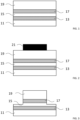
- THE figures 1 to 5 are sectional views illustrating successive steps of an example of a process for manufacturing a capacitor according to one embodiment.
- FIG. 1 represents a starting stack comprising, successively, from a lower face of the stack, a first conductive layer 11, a first electrode 13, a first dielectric layer 15, a second electrode 17, and a second conductive layer 19.
- the stack is carried by a support not shown.
- the support makes it possible, for example, to carry other elements such as inductors or resistors formed near the capacitor.
- the support is, for example a glass or silicon substrate, preferably highly resistive.
- the support is, for example separated from the conductive layer 11 by a dielectric layer, for example an oxide layer, for example undoped silicon glass or any other silicon oxide.
- the first conductive layer 11, also called redistribution layer or RDL is, for example, made of a metallic material.
- the conductive layer 11 is made of aluminum or an aluminum-based alloy.
- the conductive layer 11 is, for example example, in an alloy of aluminum and copper (AlCu) or in an alloy of aluminum, copper and silicon (AlSiCu).
- the conductive layer 11 has a thickness of between 0.5 ⁇ m and 3 ⁇ m, for example of the order of 1.5 ⁇ m.
- the first electrode 13 is, for example, located on and in contact with the conductive layer 11.
- the electrodes 13 and 17 can be made of the same material or of different materials.
- the electrodes 13 and 17 can, for example, be made of tantalum nitride (TaN).
- the electrodes 13 and 17 can be made of polycrystalline silicon or platinum.
- the electrode 13 has a thickness of between 20 nm and 200 nm, preferably of the order of approximately 80 nm.
- the electrode 17 has a thickness of between 20 nm and 200 nm, preferably of the order of approximately 80 nm.
- electrode 13 has a thickness equal to the thickness of electrode 17.
- Electrodes 13 and 17, also called lower and upper electrodes respectively, are separated by dielectric layer 15.
- dielectric layer 15 is located on and in contact with electrode 13 and electrode 17 is located on and in contact with the dielectric layer 15.
- the layer 15 is made of a dielectric material.
- the dielectric layer 15 is made of silicon nitride (Si 3 N 4 ) or tantalum nitride oxide (TaON).
- the dielectric layer 15 has, for example a thickness of between 20 nm and 600 nm, for example of the order of 100 nm, of the order of 175 nm or of the order of 400 nm.
- the electrode 17 is surmounted by the conductive layer 19.
- the conductive layer 19 is located on and in contact with the electrode 17.
- the conductive layer 19 is made of a metallic material. More precisely, the conductive layer 19 is a metallic material that can be etched by plasma.
- the conductive layer 19 is made of aluminum, copper, platinum, tungsten, titanium or an alloy based on one of these materials such as a copper-titanium alloy (TiCu), a copper-aluminum alloy (AlCu) or a titanium-tungsten alloy (TiW).
- layer 19 has a thickness of between 20 nm and 600 nm, for example of the order of 400 nm.
- the layers and electrodes 13, 15, 17 and 19 are aligned vertically. In particular, they each extend above the entire upper surface of the conductive layer 11.
- figure 2 illustrates a structure obtained at the end of a step of depositing a masking layer 21 on the front face of the stack illustrated in figure 1 .
- the masking layer 21 is deposited, for example by centrifugation, on the upper face of the structure, that is to say the front face of the structure in the orientation of the figure 2 . More precisely, the masking layer 21 is deposited on and in contact with the upper face of the conductive layer 19.
- the masking layer 21 is removed locally, for example by photolithography.
- the masking layer 21 is removed locally so that it only remains facing a central part of the stack, and more particularly facing a part of the stack where the capacitor will be formed.
- the masking layer 21 is for example made of a photosensitive resin.
- FIG. 3 illustrates a structure obtained at the end of a step of engraving an upper part of the structure illustrated in figure 2 .
- the etching corresponds to chemical plasma etching, for example using a plasma based on chlorine and/or fluorine using the masking layer 21 as an etching mask.
- the conductive layer 19, the electrode 17 and part of the thickness of the dielectric layer 15 are removed in a peripheral part of the stack, that is to say outside of the masking layer 21.
- the portions of the conductive layer 19 and the electrode 17 not covered by the masking layer 21 are completely removed. and only part of the thickness of the dielectric layer 15 in its portion not covered by the masking layer 21.
- approximately 50% of the thickness of the dielectric layer 15 remains outside of the masking layer 21.
- approximately 20 nm of the dielectric layer 15 remains outside of the masking layer 21.
- the masking layer 21 is removed at the end of the step of etching the semiconductor layer 19, the electrode 17 and the dielectric layer 15.
- FIG 4 illustrates a structure obtained at the end of a step of depositing a second dielectric layer 23 on the upper face of the structure illustrated in Figure 3 .
- layer 23 is more precisely deposited on the upper face of layer 19, on the sides of layer 19, on the sides of electrode 17, on the part of the upper face of layer 15 not covered by layer 17 and on the sides of layer 15.
- layer 23 is deposited in a conformal manner, that is to say it is deposited over the entire upper face of the structure with a uniform thickness.
- the thickness of layer 23 is between 20 nm and 200 nm, for example of the order of 100 nm.
- the dielectric layers 15 and 23 are, for example, made of the same material.
- the dielectric layers 15 and 23 are made of different materials.
- Layer 23 is made of a dielectric material, for example a nitride or an oxide.
- layer 23 is made of tetraethyl orthosilicate or TEOS (from the English "TetraEthylOrthoSilicate"), silicon nitride or tantalum oxynitride.
- the dielectric layers 15 and 23 are made of the same material and are formed with the same thickness.
- FIG. 5 illustrates a structure obtained at the end of a step of engraving the structure illustrated in Figure 4 .
- the etching of this step corresponds to vertical anisotropic chemical plasma etching.
- the engraving is directive, it is carried out mainly in a single preferential direction, here the vertical direction in the orientation of the figure.
- the etching is carried out using a fluorine-based plasma.
- this etching step is selective and makes it possible to remove part of the dielectric layer 23, part of the electrode 13, part of the dielectric layer 15 but it has no or little effect on the conductive layer 19 which remains.
- the etching step is, for example, stopped when the upper face of the conductive layer 11 is revealed in the peripheral part of the stack. Layers 23 and 15 and electrode 13 are therefore removed successively.
- the dielectric layer 23 is therefore removed in the central part of the stack, that is to say opposite the conductive layer 19. Still during this step, the electrode 13 and the dielectric layers 15 and 23 are removed in the peripheral part of the stack. Again during this step, between the central part and the peripheral part, part of the dielectric layer 23 located on the sides of the conductive layer 19 is removed.
- the upper face of the conductive layer 19 and the upper face of the dielectric layer 23 are not aligned, the upper face of the layer 23 being set back relative to the upper face of layer 19.
- This shift is explained by the fact that there is more material which can be removed, by plasma etching, in the peripheral part of the stack than in the central part of the stack. Indeed, when the dielectric layer 23 has been removed to a thickness corresponding to the thickness located in the central part of the stack, the etching continues, the dielectric layer 23 formed on the sides of the conductive layer 19 is then removed.
- the difference in level between the upper face of layer 19 and the upper face of layer 23 is of the order of 40 nm.
- the structure comprises a central part comprising successively, on the upper face of the conductive layer 11, the electrode 13, the dielectric layer 15, the electrode 17 and the conductive layer 19.
- the electrode 13 and part of the layer 15 extend beyond the sides of the layer 19 and are surmounted by the layer 23 formed on part of the sides of the layers 19 and 15 and the electrode 17, so that the sides of the electrode 13 and of the layer 15 are aligned with the sides of the layer 23.
- the etching speed of the electrode 13 may be slightly higher than that of the layers 15 and 23.
- the etching step may create a slight shrinkage (not shown) of the side of the the electrode 13 relative to the side of the layers 15 and 23.
- a metal pad not shown, for example made of copper, is for example placed on the upper face of the conductive layer 19.
- An advantage of this embodiment is that it makes it possible to form a capacitor at a limited cost insofar as the method comprises a single photolithography step.
- Another advantage of this embodiment is that it makes it possible to reduce the gap between the side of the conductive layer 19 and the side of the electrode 13, due to the protection conferred by the dielectric layer 23 on the sides of the layers 15 and 19.
Landscapes
- Engineering & Computer Science (AREA)
- Power Engineering (AREA)
- Microelectronics & Electronic Packaging (AREA)
- Manufacturing & Machinery (AREA)
- Chemical & Material Sciences (AREA)
- Ceramic Engineering (AREA)
- Inorganic Chemistry (AREA)
- Materials Engineering (AREA)
- Semiconductor Integrated Circuits (AREA)
- Physics & Mathematics (AREA)
- Plasma & Fusion (AREA)
- Ceramic Capacitors (AREA)
- Fixed Capacitors And Capacitor Manufacturing Machines (AREA)
Applications Claiming Priority (1)
| Application Number | Priority Date | Filing Date | Title |
|---|---|---|---|
| FR2210596A FR3140984A1 (fr) | 2022-10-14 | 2022-10-14 | Procédé de fabrication d'un condensateur |
Publications (1)
| Publication Number | Publication Date |
|---|---|
| EP4354476A1 true EP4354476A1 (de) | 2024-04-17 |
Family
ID=85222106
Family Applications (1)
| Application Number | Title | Priority Date | Filing Date |
|---|---|---|---|
| EP23201024.9A Pending EP4354476A1 (de) | 2022-10-14 | 2023-09-29 | Verfahren zur herstellung eines kondensators |
Country Status (4)
| Country | Link |
|---|---|
| US (1) | US20240128311A1 (de) |
| EP (1) | EP4354476A1 (de) |
| CN (1) | CN117894603A (de) |
| FR (1) | FR3140984A1 (de) |
Citations (6)
| Publication number | Priority date | Publication date | Assignee | Title |
|---|---|---|---|---|
| US20030129771A1 (en) * | 2001-12-31 | 2003-07-10 | Summerfelt Scott R. | Method of forming an FeRAM capacitor having a bottom electrode diffusion barrier |
| KR20060114056A (ko) * | 2005-04-27 | 2006-11-06 | 삼성전자주식회사 | 평판형 금속-절연체-금속 캐패시터의 제조방법 |
| KR100866683B1 (ko) * | 2007-05-18 | 2008-11-04 | 주식회사 동부하이텍 | 반도체 소자의 캐패시터 형성 방법 |
| JP2010153855A (ja) * | 2008-12-24 | 2010-07-08 | Magnachip Semiconductor Ltd | キャパシタ及びその製造方法 |
| US20110108951A1 (en) * | 2008-12-24 | 2011-05-12 | Magnachip Semiconductor, Ltd. | Semiconductor device with mim capacitor and method for manufacturing the same |
| US20200006470A1 (en) * | 2018-06-27 | 2020-01-02 | Taiwan Semiconductor Manufacturing Co., Ltd. | Electronic device including a capacitor |
Family Cites Families (1)
| Publication number | Priority date | Publication date | Assignee | Title |
|---|---|---|---|---|
| US12388039B2 (en) * | 2022-04-11 | 2025-08-12 | Taiwan Semiconductor Manufacturing Company, Ltd. | 3D IC comprising semiconductor substrates with different bandgaps |
-
2022
- 2022-10-14 FR FR2210596A patent/FR3140984A1/fr active Pending
-
2023
- 2023-07-24 US US18/357,898 patent/US20240128311A1/en active Pending
- 2023-09-28 CN CN202311276873.0A patent/CN117894603A/zh active Pending
- 2023-09-29 EP EP23201024.9A patent/EP4354476A1/de active Pending
Patent Citations (6)
| Publication number | Priority date | Publication date | Assignee | Title |
|---|---|---|---|---|
| US20030129771A1 (en) * | 2001-12-31 | 2003-07-10 | Summerfelt Scott R. | Method of forming an FeRAM capacitor having a bottom electrode diffusion barrier |
| KR20060114056A (ko) * | 2005-04-27 | 2006-11-06 | 삼성전자주식회사 | 평판형 금속-절연체-금속 캐패시터의 제조방법 |
| KR100866683B1 (ko) * | 2007-05-18 | 2008-11-04 | 주식회사 동부하이텍 | 반도체 소자의 캐패시터 형성 방법 |
| JP2010153855A (ja) * | 2008-12-24 | 2010-07-08 | Magnachip Semiconductor Ltd | キャパシタ及びその製造方法 |
| US20110108951A1 (en) * | 2008-12-24 | 2011-05-12 | Magnachip Semiconductor, Ltd. | Semiconductor device with mim capacitor and method for manufacturing the same |
| US20200006470A1 (en) * | 2018-06-27 | 2020-01-02 | Taiwan Semiconductor Manufacturing Co., Ltd. | Electronic device including a capacitor |
Also Published As
| Publication number | Publication date |
|---|---|
| FR3140984A1 (fr) | 2024-04-19 |
| US20240128311A1 (en) | 2024-04-18 |
| CN117894603A (zh) | 2024-04-16 |
Similar Documents
| Publication | Publication Date | Title |
|---|---|---|
| EP1365444B1 (de) | Grabenkondensator mit zwei vom Substrat unabhängigen Elektroden | |
| EP2816624B1 (de) | Verfahren zur Herstellung einer Substratdurchkontaktierung und eines durchgehenden Kondensators in einem Substrat | |
| EP4002441A2 (de) | Elektronischer schaltkreis für eine hybride molekülverbindung | |
| EP1111669A1 (de) | Verfahren zur Herstellung von isolierten metallischen Verbindungsleitungen in integrierten Schaltkreisen | |
| EP3876288A1 (de) | Bildung eines thyristors, triacs oder einer diode zur unterdrückung von transienten spannungen | |
| EP3913657A2 (de) | Verfahren zur verarbeitung einer elektronischen schaltung für hybride molekulare klebung | |
| EP1180789A1 (de) | Herstellung eines Kondensators im Inneren einer integrierten Schaltung und entsprechende integrierte Schaltung | |
| EP0892442B1 (de) | Verfahren zur Herstellung einer Metall-Metall-Kapazität in einer integrierten Schaltung und entsprechende integrierte Schaltung | |
| EP4354476A1 (de) | Verfahren zur herstellung eines kondensators | |
| EP4220674A1 (de) | Vertikaler kondensator | |
| FR3093592A1 (fr) | Circuit intégré comportant un condensateur tridimensionnel | |
| FR2763424A1 (fr) | Processus de damasquinage double | |
| EP4012735B1 (de) | Verfahren zur herstellung eines kondensators | |
| FR3112421A1 (fr) | Procédé de réalisation d’une structure d’isolation | |
| EP4152373A2 (de) | Verfahren zur herstellung eines elektronischen schaltkreises für die selbstmontage an einem anderen elektronischen schaltkreis | |
| EP1180790B1 (de) | Kondensatorherstellung mit metallischen Elektroden | |
| EP4383292A1 (de) | Verfahren zur herstellung eines kondensators | |
| EP3832707A1 (de) | Verbindungsstruktur eines phasenwechselspeichers | |
| EP4095935B1 (de) | Herstellungsverfahren eines speichers mit phasenänderung | |
| EP4593074A1 (de) | Elektronisches bauelement mit anschlusssäulen | |
| FR2789803A1 (fr) | Procede de realisation d'une connexion metallique verticale dans un circuit integre | |
| FR3133516A1 (fr) | Condensateur | |
| EP4350761A1 (de) | Elektronischer chip mit einer ubm-metallisierung | |
| WO2024126599A1 (fr) | Procédé de préparation d'un empilement en vue d'un collage | |
| EP4195246A1 (de) | Verfahren zur herstellung eines vias |
Legal Events
| Date | Code | Title | Description |
|---|---|---|---|
| PUAI | Public reference made under article 153(3) epc to a published international application that has entered the european phase |
Free format text: ORIGINAL CODE: 0009012 |
|
| STAA | Information on the status of an ep patent application or granted ep patent |
Free format text: STATUS: REQUEST FOR EXAMINATION WAS MADE |
|
| 17P | Request for examination filed |
Effective date: 20230929 |
|
| AK | Designated contracting states |
Kind code of ref document: A1 Designated state(s): AL AT BE BG CH CY CZ DE DK EE ES FI FR GB GR HR HU IE IS IT LI LT LU LV MC ME MK MT NL NO PL PT RO RS SE SI SK SM TR |