EP3787007B1 - Kontaktanschluss auf germanium - Google Patents
Kontaktanschluss auf germanium Download PDFInfo
- Publication number
- EP3787007B1 EP3787007B1 EP20192014.7A EP20192014A EP3787007B1 EP 3787007 B1 EP3787007 B1 EP 3787007B1 EP 20192014 A EP20192014 A EP 20192014A EP 3787007 B1 EP3787007 B1 EP 3787007B1
- Authority
- EP
- European Patent Office
- Prior art keywords
- layer
- germanium
- semiconductor
- region
- opening
- Prior art date
- Legal status (The legal status is an assumption and is not a legal conclusion. Google has not performed a legal analysis and makes no representation as to the accuracy of the status listed.)
- Active
Links
Images


Classifications
-
- H—ELECTRICITY
- H10—SEMICONDUCTOR DEVICES; ELECTRIC SOLID-STATE DEVICES NOT OTHERWISE PROVIDED FOR
- H10D—INORGANIC ELECTRIC SEMICONDUCTOR DEVICES
- H10D64/00—Electrodes of devices having potential barriers
- H10D64/01—Manufacture or treatment
- H10D64/011—Manufacture or treatment of electrodes ohmically coupled to a semiconductor
- H10D64/0111—Manufacture or treatment of electrodes ohmically coupled to a semiconductor to Group IV semiconductors
- H10D64/0112—Manufacture or treatment of electrodes ohmically coupled to a semiconductor to Group IV semiconductors using conductive layers comprising silicides
-
- H—ELECTRICITY
- H10—SEMICONDUCTOR DEVICES; ELECTRIC SOLID-STATE DEVICES NOT OTHERWISE PROVIDED FOR
- H10F—INORGANIC SEMICONDUCTOR DEVICES SENSITIVE TO INFRARED RADIATION, LIGHT, ELECTROMAGNETIC RADIATION OF SHORTER WAVELENGTH OR CORPUSCULAR RADIATION
- H10F30/00—Individual radiation-sensitive semiconductor devices in which radiation controls the flow of current through the devices, e.g. photodetectors
- H10F30/20—Individual radiation-sensitive semiconductor devices in which radiation controls the flow of current through the devices, e.g. photodetectors the devices having potential barriers, e.g. phototransistors
- H10F30/21—Individual radiation-sensitive semiconductor devices in which radiation controls the flow of current through the devices, e.g. photodetectors the devices having potential barriers, e.g. phototransistors the devices being sensitive to infrared, visible or ultraviolet radiation
- H10F30/22—Individual radiation-sensitive semiconductor devices in which radiation controls the flow of current through the devices, e.g. photodetectors the devices having potential barriers, e.g. phototransistors the devices being sensitive to infrared, visible or ultraviolet radiation the devices having only one potential barrier, e.g. photodiodes
- H10F30/223—Individual radiation-sensitive semiconductor devices in which radiation controls the flow of current through the devices, e.g. photodetectors the devices having potential barriers, e.g. phototransistors the devices being sensitive to infrared, visible or ultraviolet radiation the devices having only one potential barrier, e.g. photodiodes the potential barrier being a PIN barrier
- H10F30/2235—Individual radiation-sensitive semiconductor devices in which radiation controls the flow of current through the devices, e.g. photodetectors the devices having potential barriers, e.g. phototransistors the devices being sensitive to infrared, visible or ultraviolet radiation the devices having only one potential barrier, e.g. photodiodes the potential barrier being a PIN barrier the devices comprising Group IV amorphous materials
-
- H—ELECTRICITY
- H10—SEMICONDUCTOR DEVICES; ELECTRIC SOLID-STATE DEVICES NOT OTHERWISE PROVIDED FOR
- H10F—INORGANIC SEMICONDUCTOR DEVICES SENSITIVE TO INFRARED RADIATION, LIGHT, ELECTROMAGNETIC RADIATION OF SHORTER WAVELENGTH OR CORPUSCULAR RADIATION
- H10F71/00—Manufacture or treatment of devices covered by this subclass
- H10F71/121—The active layers comprising only Group IV materials
- H10F71/1212—The active layers comprising only Group IV materials consisting of germanium
-
- H—ELECTRICITY
- H10—SEMICONDUCTOR DEVICES; ELECTRIC SOLID-STATE DEVICES NOT OTHERWISE PROVIDED FOR
- H10F—INORGANIC SEMICONDUCTOR DEVICES SENSITIVE TO INFRARED RADIATION, LIGHT, ELECTROMAGNETIC RADIATION OF SHORTER WAVELENGTH OR CORPUSCULAR RADIATION
- H10F71/00—Manufacture or treatment of devices covered by this subclass
- H10F71/121—The active layers comprising only Group IV materials
- H10F71/1215—The active layers comprising only Group IV materials comprising at least two Group IV elements, e.g. SiGe
-
- H—ELECTRICITY
- H10—SEMICONDUCTOR DEVICES; ELECTRIC SOLID-STATE DEVICES NOT OTHERWISE PROVIDED FOR
- H10F—INORGANIC SEMICONDUCTOR DEVICES SENSITIVE TO INFRARED RADIATION, LIGHT, ELECTROMAGNETIC RADIATION OF SHORTER WAVELENGTH OR CORPUSCULAR RADIATION
- H10F77/00—Constructional details of devices covered by this subclass
- H10F77/20—Electrodes
- H10F77/206—Electrodes for devices having potential barriers
-
- H—ELECTRICITY
- H10—SEMICONDUCTOR DEVICES; ELECTRIC SOLID-STATE DEVICES NOT OTHERWISE PROVIDED FOR
- H10F—INORGANIC SEMICONDUCTOR DEVICES SENSITIVE TO INFRARED RADIATION, LIGHT, ELECTROMAGNETIC RADIATION OF SHORTER WAVELENGTH OR CORPUSCULAR RADIATION
- H10F77/00—Constructional details of devices covered by this subclass
- H10F77/93—Interconnections
- H10F77/933—Interconnections for devices having potential barriers
Definitions
- This description relates generally to electronic devices, and more particularly to electronic components comprising germanium and to methods of manufacturing electronic components.
- a PIN-type photodiode i.e. a photodiode comprising an intrinsic semiconductor region between N- and P-type doped semiconductor regions, may be based on germanium.
- the photodiode can then detect optical radiation with wavelengths between 0.9 ⁇ m and 1.5 pm.
- a region comprising germanium is intended to be electrically connected to other devices by a conductive bond. Electrical contact between this region and the conductive bond is ensured by a contact area, or contact socket.
- US2007148966 describes a method of fabricating an interconnect on a substrate containing germanium.
- One embodiment overcomes all or part of the drawbacks of known contact connections with a semiconductor region comprising germanium.
- One embodiment overcomes all or part of the drawbacks of known methods of making contact with a semiconductor region comprising germanium.
- One embodiment overcomes all or part of the drawbacks of the methods of etching an opening in an insulator covering a semiconductor region comprising germanium.
- One embodiment overcomes some or all of the drawbacks of known PIN type photodiodes comprising an intrinsic germanium region.
- one embodiment provides a photodiode having a reduced dark current.
- an embodiment provides a method of forming an electrical contact with a semiconductor region consisting primarily of germanium according to claim 1.
- One embodiment provides a photodiode formed by a method as defined above.
- the expressions “approximately”, “approximately”, “substantially”, and “of the order of” mean to within 10%, preferably to within 5%.
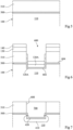
- FIGS. 1 to 4 are partial and schematic sectional views showing steps of an embodiment of a method of manufacturing a contact on a region comprising germanium.
- the method is implemented during the manufacture of an electronic device comprising one or more components comprising or based on germanium.
- the device may comprise, or be constituted by, an integrated circuit electronic chip.
- Such a chip is defined by a portion of a semiconductor wafer and elements, such as electronic components, integrally located in and on one face of the wafer.
- the method may be implemented for the manufacture of a photodiode comprising germanium.
- the substrate 100 may be constituted by a portion of a semiconductor wafer, for example made of germanium.
- the substrate 100 may also be constituted by a layer covering the upper face of a support such as, for example, a semiconductor wafer.
- a semiconductor region 110 comprising germanium is located on the side of a face of the substrate 100, for example the front or upper face of the substrate 100.
- the region 110 is for example a doped region of the substrate.
- the semiconductor region 110 may have been formed for example in a cavity etched in the substrate 100.
- the semiconductor region 110 is monocrystalline, the substrate 100 preferably being monocrystalline. The semiconductor region 110 may then result from epitaxy.
- the region 110 is mainly, i.e. predominantly, made of germanium.
- the region 110 is made of a semiconductor material having an atomic percentage of germanium greater than 50%, preferably greater than 90%.
- the region 110 is made of germanium, for example doped. More preferably, the region 110 is made of germanium. monocrystalline.
- the 110 region is made of silicon-germanium, for example doped.
- a semiconductor layer 120 having an atomic percentage of silicon greater than 70% is formed on the semiconductor region 110.
- the layer 120 may comprise, in addition to silicon, a metalloid other than silicon, preferably germanium.
- the layer 120 is made of silicon.
- the layer 120 is made of silicon-germanium.
- the semiconductor layer 120 is monocrystalline.
- the layer 120 can be obtained by epitaxy on the monocrystalline region 110.
- the thickness of the semiconductor layer 120 is less than a thickness threshold allowing the epitaxied layer to be monocrystalline.
- This thickness threshold can be determined experimentally as a function of the composition of the semiconductor layer 120 and the semiconductor region 110. This threshold is of the order of 2 nm for a silicon layer 120 epitaxied on the germanium region 110.
- the semiconductor layer 120 is not monocrystalline. The thickness of the layer 120 can then be greater than the thickness threshold.
- the metal layer 130 comprises nickel, for example is substantially made of nickel, for example is made of nickel.
- the layer 130 comprises, in addition to nickel, platinum and/or cobalt.
- the metal of the layer 130 comprises, more preferably is made of, nickel and cobalt, the atomic percentage of cobalt being between 5 and 20%.
- the metal of the layer 130 comprises, more preferably is made of, nickel and platinum, the atomic percentage of platinum being between 5 and 15%.
- the thickness of the metal layer 130 is greater than half that of the semiconductor layer 120. More preferably, the metal layer 130 has a thickness of between 7 and 50 nm.
- the upper surface of the semiconductor layer 120 has been prepared beforehand.
- the surface preparation step comprises, for example, a liquid phase treatment based on hydrofluoric acid, then a plasma treatment.
- the plasma may be based on argon, or, for example, of the type known under the trade name Siconi TM .
- the plasma treatment and the deposition of the metal layer 130 are then carried out successively without breaking the vacuum. This makes it possible to avoid the presence of impurities, such as oxides, between the semiconductor layer 120 and the metal layer 130. Such impurities could come from exposure to air after the deposition step of the layer 120, or after the liquid phase surface preparation step.
- the semiconductor layer 120 and the metal layer 130 are therefore in direct contact with each other.
- a protective layer 140 is formed on the layer 130. This layer is then preferably formed without breaking the vacuum after the deposition of the metal layer 130.
- the layer 140 is intended to protect the structures located under the layer 140 against oxidation during subsequent steps of the method.
- the protective layer 140 is made of titanium nitride. Alternatively, the protective layer 140 may be omitted.
- a first heat treatment is carried out. More precisely, this treatment thermal corresponds to an annealing of the structure obtained from the figure 1 .
- This first heat treatment is carried out at a temperature allowing the metal of the metal layer 130 to react partially with the material of the semiconductor layer 120. A layer 220 is thus obtained in place of the layer 120.
- the temperature of the first heat treatment is preferably less than or equal to 300°C, for example between 250°C and 300°C, which allows a partial reaction of the layer 130 comprising nickel with the material of the semiconductor layer 120.
- the first heat treatment is carried out in the presence of nitrogen.
- the nitrogen is preferably at atmospheric pressure or at a pressure less than 1 bar higher than atmospheric pressure.
- the duration of the first heat treatment is preferably between 10 s and 120 s.
- the layer 220 preferably comprises, and is constituted by, an intermetallic material, or intermetallic compound, i.e. the combination of one or more metallic chemical elements and one or more chemical elements, typically metalloids, that can be included in the composition of a semiconductor.
- the intermetallic material has a crystalline structure combining the metallic and non-metallic chemical elements.
- the non-metallic chemical elements are substantially constituted by the material of the semiconductor layer 120.
- the fact that more than 70% of the atoms of the semiconductor layer 120 are silicon implies that more than 70% of the non-metallic atoms of the layer 220 are silicon.
- the intermetallic material of the layer 220 is a nickel silicide or a silicide comprising nickel. In another preferred example, the intermetallic material of the layer 220 is a nickel germano-silicide or a nickel-containing germano-silicide.
- the thickness of the metal layer 130 chosen at the step of figure 1 is sufficient for a portion of the metal of layer 130 to react with an upper portion of semiconductor region 110.
- This reaction produces a layer 210 located below layer 220.
- Layer 210 preferably comprises an intermetallic material. Because region 110 is primarily germanium, the nonmetal atoms of layer 210 are primarily germanium atoms. Thus, when metal layer 130 is nickel or includes nickel, the intermetallic material of layer 210 is nickel germanide or a germanide including nickel.
- the thickness of the metal layer 130 chosen at the step of figure 1 is sufficient so that a portion 230 of the metal layer 130 does not react with the semiconductor layer 120 and the semiconductor region 110.
- the possible protective layer 140 is removed, as well as the part 230 of the layer 130 which has not reacted.
- This removal is selective with respect to the material of the layer 220.
- the removal is for example carried out in an etching solution based on sulfuric acid and hydrogen peroxide, or for example in an etching solution based on hydrochloric acid and nitric acid. Because the layer 220 comprises, apart from the metallic elements, more than 70% of silicon atoms, these solutions make it possible to etch the materials of the layers 130 and 140 without removing or altering the layer 220.
- a second heat treatment is carried out.
- This heat treatment corresponds to an annealing of the structure obtained at the stage of the figure 3 .
- the temperature of the heat treatment is preferably greater than or equal to 390°C.
- the phase of the intermetallic material of the layer 420 has an electrical resistivity lower than that of the other phases of this intermetallic.
- the layer 420 comprises the same proportion of metal atoms as non-metal atoms, for example comprises the same atomic proportions of nickel and silicon (NiSi).
- NiSi nickel and silicon
- a portion of the nickel contained in the layer 220 at the step of figure 3 reacts with the semiconductor region 110 during the second annealing.
- the thickness of the layer 410 is then greater than that of the layer 210 ( Figures 2 and 3 ).
- layer 210 is not formed during the first heat treatment, and only layer 410 is formed during the second heat treatment.
- the thickness of the metal layer 130 is preferably greater than half that of the semiconductor layer 120, makes it possible to obtain the layer 410 during the second heat treatment.
- the heat treatment temperature is preferably less than 420°C. This makes it possible to optimize the resistivity of the nickel germanide of the layer 410, and to avoid deteriorating this resistivity by too high a temperature.
- the intermetallic zones defined by the layers 410 and 420 thus obtained constitute an electrical contact 400 on the semiconductor region 110.
- the presence of the 420 layer makes it possible to obtain a 400 contact on the germanium having better resistivity and reliability than a contact without such a layer.
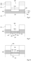
- FIGS. 5 to 7 are partial, schematic sectional views showing steps of another embodiment of a method of manufacturing a contact on a semiconductor region 110 comprising germanium.
- the semiconductor region 110 is identical or similar to that described in relation to the figure 1 , and is preferentially located in the upper part of a substrate 100.
- a semiconductor layer 500 comprising silicon is formed on the upper surface of the semiconductor region 110.
- the layer 500 is made of silicon, or has an atomic percentage of silicon greater than 70%.
- the layer 500 is grown by epitaxy on the surface of the semiconductor region 110.
- the thickness of the layer 500 is for example between 1 nm and 3 nm, preferably of the order of 2 nm.
- the insulating layer 510 may be made of silicon oxide, preferably silicon dioxide, more preferably resulting from a hydrolysis of tetraethyl orthosilicate (TEOS).
- TEOS tetraethyl orthosilicate
- the insulating layer of silicon oxide 510 is a passivation layer.
- the thickness of the insulating layer 510 is of the order of, or greater than, 100 nm.
- an opening 600 is etched passing through the insulating layer 510 from one side to the other at the location of the future contact point.
- the opening 600 is made only above a portion of the semiconductor region 110.
- the width of the opening may be between 300 nm and 1.5 ⁇ m.
- the opening 600 is compatible with any conventional method for obtaining an opening in an insulating layer, for example photolithography followed by plasma etching (the etching mask is not shown).
- the opening 600 is extended through the layer 500 to a level located in the semiconductor region 110.
- the level difference i.e. the distance in the direction orthogonal to the upper face of the substrate 100, between the bottom 602 of the opening 600 and the upper face 604 of the semiconductor layer 500, is for example between 5 nm and 30 nm, preferably of the order of 10 nm.
- a 120A semiconductor layer is then grown by epitaxy.
- the 120A layer is identical in composition and thickness to the 120 semiconductor layer of the process of Figures 1 to 4 .
- the semiconductor layer 120A grows from the bottom 602 and the portions of the side walls of the opening 600 located below the upper level 604 of the layer 500.
- the semiconductor region defined by the layer 120A forms, with the remaining portions of layer 500, a continuous semiconductor layer, that is to say devoid of openings, covering the semiconductor region 110, this continuous layer comprising at least 70% silicon.
- the metal layers 130 and possibly the protective layers 140 described in relation to the figure 1 cover the bottom of the opening 600 and the remaining portions of the insulating layer 510.
- the total thickness of the metal 130 and protective 140 layers is less than that of the insulating layer 510.
- the metal 130 and protective 140 layers are formed by non-conformal deposition, that is to say that the materials of these layers are only deposited on the surfaces facing upwards. Because the thickness of the metal layer 130 is less than that of the insulating layer 510, this results in a metal region 130A without contact with the rest of the layer 130, and located at the bottom of the opening 600.
- the step described here is not limiting, and any method allowing a metal region 130A to be formed on only part of the semiconductor region 110 can be used.
- the metal layers 130 and/or the protective layers 140 can be formed by conformal deposition.
- the metal layer 130 is chosen to be sufficiently thick to form, under the zone 420, an intermetallic zone 410, in which the non-metallic atoms are mainly germanium. More preferably, the zone 410 comprises, for example is constituted by, nickel germanide.
- the opening 600 is filled with an electrical conductor 700.
- the conductor 700 makes it possible to establish an electrical connection with the semiconductor region 110.
- the conductor 700 can be covered with, and in contact with, an electrical connection track between components of an electronic chip.
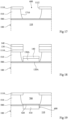
- THE figures 8 to 10 are partial, schematic sectional views showing steps of another embodiment of a method of forming a localized contact area on a semiconductor region 110 comprising germanium.
- the semiconductor region 110 is identical to that described in relation to the figure 1 .
- the semiconductor region 110 is preferably located on the front face side of a substrate 100.
- the semiconductor region 110 is covered with a multilayer 800 comprising, alternately, layers 802 of silicon and layers 804 of germanium. More precisely, the layers 802 have an atomic proportion of silicon greater than 70%. Preferably, the layers 802 are made of silicon, or of silicon-germanium having an atomic proportion of silicon greater than 70%.
- the layers 804 are made of germanium or are mainly composed of germanium. Preferably, the layers 804 are made of germanium, or of silicon-germanium mainly composed of germanium.
- the thickness of the multilayer 800 is greater than 10 nm, preferably of the order of 15 nm.
- the layers 802 have the same thickness.
- the layers 804 have the same thickness. More preferably, the layers 802 and 804 all have the same thickness.
- the multilayer 800 is formed by epitaxy on the upper surface of the monocrystalline region 110.
- Each of the layers 802 and 804 then has a thickness less than a thickness threshold below which the layer remains monocrystalline.
- this threshold or critical thickness, depends on the composition of the layers 802 and 804.
- each of the layers 802 and 804 has a thickness of the order of, or less than, 2 nm.
- the multilayer 800 obtained is monocrystalline.
- the opening 600 extends to a level located inside the multilayer 800.
- the bottom of the opening 600 is located in a layer 804A among the layers 804 consisting mainly of germanium.
- the bottom of the opening 600 stops inside one of the layers 802, or at an interface between one of the layers 802 and one of the layers 804. At least one of the layers 802 comprising at least 70% silicon is not reached by the opening 600 and is therefore left intact.
- two of the layers 802 are not etched.
- the thickness of the metal layer 130 deposited in the step of figure 8 is chosen to be sufficient so that each of the layers 802 and 804, as well as a portion of the semiconductor region 110, reacts with the metal of the metal layer 130.
- the reaction of each of the layers 802, 804 with the material of the metal region 130A produces a zone 902 under the opening 600.
- the portions of the structure located between the zones 902 and the remainder of the multilayer 800, delimited in the figure by dotted lines 910, are not shown.
- layer 904A (shown in dotted lines) is also removed, which results from the reaction of layer 804A with the material of the metal layer 130.
- This removal is preferably carried out with the same etching solution as that used to remove the remaining parts of the metal region 130A.
- the non-metal atoms of the region 904A are mainly germanium atoms. This makes it possible to avoid retaining the region 904A which would have been damaged by the etching solution.
- the upper face of the area 902 that was under and in contact with the area 904A before removal is thus made accessible. Because more than 70%, or all, of the non-metal atoms in the area 902 are silicon, the etching solution leaves the area 902 intact. The area 902 is therefore not damaged by the etching.
- the semiconductor region 110 is protected from the etching solution by at least one of the areas 902.
- the remainder of the cavity of the opening 600 is then filled with an electrical conductor 700, preferably metallic.
- the area 1002 located in the upper part of the contact point is in electrical contact with the conductor 700. Since the area 902 ( figure 9 ) upper has not been altered upon removal of the unreacted portions of the metal layer 130, and since there is no intermetallic region from region 904A between region 1002 and electrical conductor 700, the resistance and reliability of the contact between the contact socket and the conductor 700 are optimized.
- the entire contact socket and the semiconductor region 110 is monocrystalline.
- the electrical resistance of the contact socket is lower than that of a non-monocrystalline contact socket. This allows for further improvement in electrical resistance.
- FIGS 11 to 15 are partial and schematic sectional views representing successive steps of an embodiment, in the example of the second embodiment ( Figures 5 to 7 ), of a method of forming an opening in the insulating layer covering a semiconductor region comprising germanium. More specifically, the method is here applied to the formation, from the structure obtained in the step of figure 5 , with an aperture of 600 ( figure 6 ) in the insulating layer 510 covering the semiconductor region 110.
- layer 510 is preferably made of silicon oxide, more preferably of silicon dioxide, even more preferably resulting from a hydrolysis of TEOS.
- layer 510 can also be made of a silicon nitride.
- an additional layer 500 semiconductor
- the semiconductor layer 500 is located under the insulating layer 510. More precisely, the semiconductor layer 500 is located between the semiconductor region 110 and the insulating layer 510. The semiconductor layer 500 is in contact with the insulating layer 510.
- the layer 500 is made of silicon, or has an atomic percentage of silicon greater than 70%, the layer 500 then being for example made of silicon-germanium. The silicon layer 500 in contact with the insulating layer 510 then makes it possible to improve the stability of the insulating layer 510, compared to a structure without the layer 500.
- a first masking layer 1110 is formed on the insulating layer 510.
- masking layer we mean a layer intended to be crossed by one or more through openings and to be used during an etching step to allow etching reagents to pass only through these openings.
- the first masking layer 1110 is made of a dielectric material, i.e. electrically insulating.
- a dielectric material i.e. electrically insulating.
- a second masking layer 1120 comprising an opening 1122 is then formed on the first masking layer 1110.
- the opening 1122 is located directly above the location of the future opening 600.
- the second masking layer 1120 is made of polymer, and preferably results from the lithography of a positive or negative resin such as a photosensitive resin.
- a through opening 1210 located in the extension of the opening 1122 of the second masking layer 1120 is etched in the first masking layer 1110.
- the etching preferably stops on the upper surface of the insulating layer 510.
- the etching stops at a level located in the insulating layer 510.
- a possible step of removing etching residues (not shown), i.e. a cleaning step, can then be implemented.
- the cleaning is carried out using a hydrofluoric acid HF solution.
- the second masking layer is removed by oxygen-based etching, typically by plasma.
- the plasma comprises only oxygen or comprises, in addition to oxygen, carbon tetrafluoride CF 4 .
- the temperature during etching is typically between 120 and 220°C.
- Such a plasma makes it possible to remove the second masking layer 1120 when it results from lithography or from any method of forming a masking layer comprising openings and removable by oxygen-based etching.
- the opening 600 is formed in the extension of the opening 1210 of the first layer masking 1110, by fluorine-based etching, i.e. etching mainly by one or more reagents comprising fluorine.
- fluorine-based etching i.e. etching mainly by one or more reagents comprising fluorine.
- the etching is substantially in the absence of oxygen, i.e. less than 5%, preferably less than 1% of the reactive molecules used for the etching are oxygen O 2 .
- oxygen O 2 oxygen
- less than 5%, more preferably less than 1% of the reactive molecules used for the etching comprise oxygen.
- the etching reagent(s) are free of oxygen.
- the etching is a reactive ion etching RIE (Reactive Ion Etching), for example by octafluorocyclobutane C 4 F 8 and/or by trifluoromethane CHF 3 .
- RIE reactive Ion Etching
- the first masking layer 1110 is in the group consisting of HfO 2 , Al 2 O 3 , AlN, ZnO, SiN, and Si 3 N 4 makes it possible to selectively etch the material of the insulating layer 510 relative to the material of the first masking layer 1110. Indeed, in the preferred case where the insulating layer is made of silicon oxide resulting from a hydrolysis of TEOS, the etching rate of the insulating layer 510 is then more than 5 times faster than the etching rate of the material of the masking layer.
- the first masking layer is made of HfO 2 or Al 2 O 3 , and the etching rate of the silicon oxide resulting from a hydrolysis of TEOS is then more than 10 times faster than the etching rate of the material of the first masking layer.
- etching residues 1410 may remain on the sides and bottom of the opening 600. can then provide a cleaning step described below in relation to the figure 15 .
- the etching residues 1410 are removed.
- an HF solution is used for this.
- the solution preferably has an HF concentration of between 0.1% and 1% mol, and is applied for a duration of between 10 and 30 s.
- the opening 600 in the insulating layer 510 covering the semiconductor region 110 is obtained.
- a single polymer masking layer could be formed directly on the insulating layer 510, the opening 600 etched, and the masking layer removed by oxygen-based etching.
- the thickness of the layer 500 mentioned above would then have been too small to prevent the layer 500 from being oxidized over its entire thickness, and a portion of the germanium in the semiconductor region 110 from also being oxidized. This would have resulted in an extension of the opening 600 below the lower level of the insulating layer 510, as mentioned above in connection with the figures 6 And 8 .
- the steps of Figures 11 to 15 allow the insulating layer 510 to protect the semiconductor layer 500 from oxidation during removal of the polymer masking layer.
- this allows a region 120A of the semiconductor layer 500 to be left in place at the bottom of the opening.
- This also allows the opening 600 to be formed without oxidizing the germanium of the semiconductor region 110. This prevents the semiconductor region 110 from being damaged by oxidation.
- any opening in any insulating layer covering a semiconductor region consisting mainly of germanium the insulating layer preferably being made of silicon oxide and more preferably of silicon oxide resulting from hydrolysis of TEOS.
- layer 500 can be omitted.
- the insulating layer can be made of silicon nitride, the person skilled in the art then being able to define the material of the first masking layer to obtain a selective fluorine-based etching of the silicon nitride relative to the masking layer.
- FIG 16 is a partial and schematic sectional view representing a fourth embodiment of a method of manufacturing a contact socket, implementing the steps of Figures 11 to 15 .
- a contact point 400 comprising an intermetallic zone 420 formed from the semiconductor region 120A ( figure 6 ).
- the intermetallic zone results from the reaction of a 130A region ( figure 6 ) of the metal layer 130 with the semiconductor region 120A.
- the steps of the Figures 11 to 15 prevent the semiconductor region 110 from being damaged by oxidation.
- the semiconductor region 110 is preferentially doped.
- the higher the doping level of the semiconductor region 110 the more sensitive this region is to oxidation, this more particularly for doping resulting from ion implantation.
- the contact socket 400 obtained thus has a lower resistance and a higher reliability than those of a contact socket for which the opening 600 has been formed by a single masking layer process.
- Region 120A which forms intermetallic region 420 by reaction with metal region 130A, is formed by a portion of semiconductor layer 500. Because semiconductor layer 500 has an atomic percentage of silicon greater than 70%, more than 70% of the nonmetal atoms in intermetallic region 420 are silicon atoms. Alternatively, region 120A comprises, or is formed by, a semiconductor layer formed on portion of semiconductor layer 500, or, in the absence of semiconductor layer 500, directly on semiconductor region 110.
- the electrical conductor 700 is preferably obtained by forming a metal layer over the entire upper surface of the structure.
- the parts of the metal layer located above the upper level of the first masking layer 1110 are then removed. This removal is for example done by chemical-mechanical polishing.
- the first masking layer 1110 can then advantageously serve as a stop layer.
- the first masking layer is made of an electrically insulating material that can be left in place, this is not limiting.
- the first masking layer 1110 is made of a conductive material and is removed after formation of the opening 600.
- the first masking layer 1110 and the metal region 130A comprise, preferably are constituted by, one or more of the same metals.
- the first masking layer 1110 can advantageously be removed at the same time as the portions of the metal layer 130 remaining after the formation of the contact.
- the first masking layer 1110 and the protective layer 140 ( figure 6 ) covering the metal region 130A comprise, preferably are constituted by, one or more of the same metals.
- the first masking layer 1110 can advantageously be removed at the same time as the protective layer 140.
- FIG 17 is a partial and schematic sectional view representing a variant of implementation of the method of Figures 11 to 15 .
- the variant of the figure 17 corresponds to the process of Figures 11 to 15 in which, at the stage of the figure 14 , the fluorine-based etching is, at least in part, implemented by an HF solution.
- the HF solution preferably has a higher concentration than that of the HF solution used in the cleaning step of the figure 15 , for example greater than 5 mol%.
- Such etching is substantially isotropic.
- the opening 600 in the insulating layer is wider than the opening 1112 in the first masking layer 1110. In other words, the sides 1710 of opening 600 are overlooked by the edges of opening 1112.
- the layer 510 is made of silicon nitride
- the fact of providing that the layer 510 is made of silicon oxide advantageously allows the etching by fluorine-based plasma to be easier and/or the shapes of the flanks and the dimensions of the opening 600 to be better controlled.
- the fluorine-based etching step can be followed by a cleaning step corresponding to the etching step. figure 15 .
- FIGS. 18 and 19 are partial and schematic sectional views showing steps of a variant of the fourth embodiment, implementing the variant of the figure 17 .
- the metal layer 130 and, preferably, the protective layer 140 are formed, in the manner described in relation to the figure 6 .
- the metal layer 130 includes a metal region 130A for reacting with the semiconductor region 120A to form an intermetallic region. Due to the overhanging shape of the walls of the openings 600 and 1112, the metal region 130A is advantageously separated from the remainder of the layer 130, which facilitates the subsequent removal of the remaining portions of the layer 130 after reaction.
- a contact is formed comprising intermetallic zones 410 and preferably 420, and the opening 600 is filled with a conductor 700, in the manner described in relation to the figure 7 .
- FIG 20 is a partial and schematic sectional view representing a fifth embodiment of a method of manufacturing a contact socket, implementing the variant of the figure 17 .
- the fifth embodiment differs from the second embodiment ( Figures 5 to 7 ) in that, at the stage of the figure 7 , an electrically conductive layer 2010 covering the contact socket 400 is formed on the bottom and the sides of the opening 600 before filling the opening 600 with the conductor 700.
- the electrically conductive layer 2010 is preferably made of titanium nitride TiN.
- the electrically conductive layer 2010 is in contact with the intermetallic zone 420.
- the thickness of the electrically conductive layer 2010 is preferably between 5 and 20 nm.
- the electrically conductive layer 2010 makes it possible to protect the upper surface of the contact point 420, in particular against diffusion of the material of the conductor 700 towards the intermetallic zone and/or against oxidation in the case where the structure is exposed to air before filling the opening 600 with the conductor 700. This reduces the resistance and increases the reliability of the contact point, compared with a contact point not covered with the conductive layer 2010.
- the layer 2010, being electrically conductive also makes it possible to make electrical contact between the contact point and the conductor 700.
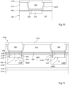
- FIG 21 is a partial and schematic sectional view showing an embodiment of a photodiode 2100. More specifically, the method of manufacturing the photodiode 2100 here implements the fifth embodiment of the method of manufacturing a contact socket. The method of manufacturing the photodiode is compatible with the various embodiments, described above, of contact making.
- the substrate 100 is made of germanium.
- the germanium of the substrate 100 is intrinsic, that is to say not intentionally doped or having a doping level of less than 10 16 atoms/cm 3 , preferably less than or equal to 10 15 atoms/cm 3 .
- the germanium of the substrate 100 is preferably monocrystalline.
- the substrate 100 may be made of silicon-germanium, preferably intrinsic and monocrystalline.
- the substrate 100 covers a semiconductor wafer 2110 of silicon. More precisely, an insulating layer 2120, typically made of silicon oxide, is arranged between the semiconductor wafer 2110 and the substrate 100.
- the semiconductor wafer 2110, the insulating layer 2120, and the substrate 100 thus define a structure of the SOI (Semiconductor On Insulator) type, more specifically, a GeOI (Germanium On Insulator) structure.
- the thickness of the insulating layer 2120 is typically of the order of 0.1 to 1 ⁇ m.
- the total thickness of the substrate 100 is for example of the order of 1 to 2 ⁇ m.
- a semiconductor region 110P made of P-type doped germanium and a semiconductor region 110N made of N-type doped germanium are formed.
- the semiconductor regions 110N and 110P are of opposite conductivity types.
- the semiconductor regions 110N and 110P extend from the free, or accessible, face of the substrate 100, i.e. the front face (upper face in the orientation of the figure).
- the semiconductor regions 110N and 110P constitute respective cathode and anode regions of the photodiode 2100.
- the semiconductor regions 110P and 110N are obtained by forming cavities in the substrate 100 at the locations of the semiconductor regions 110P and 110N, then filling the cavities by epitaxy of doped germanium. This allows the semiconductor regions to be, at least in an upper part intended for the formation of the contact points, monocrystalline.
- the semiconductor regions 110N and 110P are obtained by ion implantation.
- a 100I semiconductor region of the substrate 100 separates the 110P and 110N semiconductor regions.
- the 100I semiconductor region is thus made of intrinsic germanium.
- the distance separating the 110P and 110N semiconductor regions is between 1 ⁇ m and 20 ⁇ m.
- a layer of silicon-germanium 2130 is formed on the structure and in particular on the intrinsic region 100I.
- the layer of silicon-germanium 2130 is preferably formed by epitaxy on the substrate 100, more precisely on the free face of the substrate 100.
- the layer of silicon-germanium 2130 is thus in contact with the substrate 100.
- the layer of silicon-germanium 2130 preferably has a thickness less than the critical thickness below which the layer of silicon-germanium 2130 remains monocrystalline during its growth by epitaxy.
- the thickness of the layer of silicon-germanium 2130 is typically less than 3 nm.
- the semiconductor layer 500 is then formed on the silicon-germanium layer 2130. More preferably, before forming the semiconductor layer 500, a layer of intrinsic germanium 2140 is formed on the silicon-germanium layer 2130.
- the germanium layer 2140 allows in particular that the layer semiconductor layer 500 is monocrystalline.
- the semiconductor layer 500 has a thickness, mentioned above, sufficiently low. Indeed, in the absence of the germanium layer 2140, the sum of the thicknesses of the silicon-germanium layer 2130 and of the semiconductor layer 500 would be too high for the semiconductor layer 500 to remain monocrystalline.
- the insulating layer 510 is then formed, then the fourth embodiment is implemented in the example shown ( figure 20 ) of the contact forming method. More specifically, the method is implemented to simultaneously form two contact points 400N and 400P with the respective semiconductor regions 110N and 110P.
- Each contact point 400N, 400P thus comprises an intermetallic zone 420, in which more than 70% of the non-metal atoms are silicon atoms, and, preferably, an intermetallic zone 410, in which the non-metal atoms are mainly germanium atoms.
- the edges of the contact points are not shown (dotted regions 2150).
- the contact may further comprise an intermetallic region 2132 located on and in contact with the intermetallic region 410.
- the intermetallic region 2132 comprises silicon atoms and germanium atoms.
- the contact may further comprise an intermetallic region 2142, in which the nonmetal atoms are primarily, preferably only, germanium atoms.
- the intermetallic region 2142 is comprised between the regions 2132 and 420.
- the silicon-germanium layer 2130 located between the semiconductor region 110I and the insulating layer 510, is in contact with the intrinsic region 100I. This makes it possible to obtain a monocrystalline interface delimiting the semiconductor region 110I. Such an interface makes it possible to reduce the dark current of the photodiode, compared to an interface having crystal defects.
- the germanium layer 2140 is located between the silicon-germanium layer 2130 and the insulating layer 510, preferably between the silicon-germanium layer 2130 and the semiconductor layer 500. Because silicon-germanium has a wider band gap than germanium, carriers present in the germanium layer 2140 cannot access the intrinsic region 110I.
- These carriers may for example come from defects at the interface of the semiconductor layer 500 with the insulating layer 510 and/or the germanium layer 2140. Because the layers 2130 and 2140 make it possible to prevent these carriers from reaching the intrinsic region 100I, the dark current of the photodiode is reduced compared to the dark current of a photodiode devoid of the layers 2130 and/or 2140.
- FIG 22 is a partial, schematic, sectional view showing another embodiment of a photodiode 2200.
- the method of manufacturing the photodiode 2200 differs from that of the photodiode 2100 of the figure 21 in that, before forming the insulating layer 510, insulating trenches 2210 have been formed delimiting, on the intrinsic region 100I, a portion 2240 of the germanium layer 2140.
- the insulating trenches 2210 are located directly above the edges of the intrinsic region 100I.
- the insulating trenches are then filled with an electrical insulator, preferably the insulator of the layer 510.
- the trenches 2210 have a width of between 100 nm and 300 nm.
- the trenches extend from the upper face of the semiconductor layer 500, through layers 500 and 2140, to the upper face of silicon-germanium layer 2130.
- trenches 2210 extend through layer 2130, for example at least to the upper face of substrate 100.
- the trenches 2210 thus constitute insulating zones delimiting a portion of the germanium layer 2140 on the intrinsic region 100I. These insulating zones are located between the germanium layer 2140 and the contact points 400N and 400P.
- the photodiode 2200 is compatible with any method of forming an intrinsic germanium layer located on the intrinsic region 100I and delimited by insulating zones located between said germanium layer 2140 and the contact points.
- the germanium layer 2140 can be formed only on the intrinsic region 100I.
- the insulating areas 2210 prevent carriers present in the germanium layer 2140, mentioned above, from reaching the contact points 400N and 400P. Thus, the insulating areas allow the photodiode 2200 to have a lower dark current than that of a photodiode, such as the photodiode 2100 of the figure 21 , devoid of the insulating zones 2210.
- embodiments of methods of forming contact sockets comprising an aperture forming step are compatible with the aperture forming steps of Figures 11 to 15 and are compatible with the training stages of opening the Figures 17 and 18 .
Landscapes
- Electrodes Of Semiconductors (AREA)
- Internal Circuitry In Semiconductor Integrated Circuit Devices (AREA)
Claims (13)
- Verfahren zum Ausbilden einer Öffnung (600) in einer Isolierschicht (510), die einen Germanium aufweisenden Halbleiterbereich (110; 110N, 110P) bedeckt, das nacheinander folgende Schritte aufweist:a) Ausbilden einer ersten Maskenschicht (1110) auf der Isolierschicht (510);b) Ausbilden einer zweiten Maskenschicht (1120) mit einer Öffnung (1122) auf der ersten Maskenschicht (1110);c) Ätzen einer Öffnung (1210) in der ersten Maskenschicht, die mit der Öffnung der zweiten Maskenschicht übereinstimmt;d) Entfernung der zweiten Maskenschicht (1120) durch Ätzen auf Sauerstoffbasis; unde) Ausbilden der Öffnung (600) der Isolierschicht (510) in Übereinstimmung mit der Öffnung der ersten Maskenschicht durch ein Ätzen, bei dem weniger als 5% der verwendeten reaktiven Moleküle Sauerstoffmoleküle sind,wobei:I) die Isolierschicht (510) auf der oberen Fläche des Halbleiterbereichs (110; 110N, 110P) angeordnet ist und mit dieser in Kontakt steht; oderII) die Isolierschicht (510) sich auf einer zusätzlichen Halbleiterschicht (500) befindet und mit dieser in Kontakt steht, wobei die zusätzliche Halbleiterschicht (500) aus Silizium besteht oder einen Atomprozentsatz an Silizium von mehr als 70% aufweist und den Halbleiterbereich (110; 110N, 110P) bedeckt.
- Verfahren nach Anspruch 1, wobei die Isolierschicht (510) aus Siliziumoxid besteht.
- Verfahren nach Anspruch 1 oder 2, wobei die erste Maskenschicht (1110) aus einem elektrisch isolierenden Material besteht, vorzugsweise aus der Gruppe gebildet aus HfO2, Al2O3, AlN, ZnO, SiN und Si3N4.
- Verfahren nach einem der Ansprüche 1 bis 3, wobei Schritt e) ein Ätzen mit einem Plasma auf der Basis von C4F8 und/oder CHF3 und/oder mit einer HF-Lösung aufweist.
- Verfahren nach einem der Ansprüche 1 bis 4, wobei die zweite Maskierungsschicht (1120) eine lithographisch hergestellte Polymerschicht ist.
- Verfahren zum Ausbilden eines Kontaktbereichs (400), das die Durchführung des Verfahrens nach einem der Ansprüche 1 bis 5 aufweist, wobei der Kontaktbereich ein Kontaktbereich mit einem gleichen Halbleiterbereich (110) ist und einen intermetallischen Bereich (420) aufweist, bei dem mehr als 70 % der Nichtmetallatome Silizium sind.
- Verfahren nach Anspruch 6, wobei das Ausbilden des intermetallischen Bereichs (420) die Reaktion eines Halbleiters mit einem Metallbereich (130A) aufweist, wobei die erste Maskenschicht (1110) und der Metallbereich (130A) dasselbe Metall aufweisen.
- Verfahren nach Anspruch 6, wobei das Ausbilden des intermetallischen Bereichs (420) die Reaktion eines Halbleiters mit einem Metallbereich (130A) aufweist, der mit einer Schutzschicht (140) bedeckt ist, wobei die erste Maskenschicht (1110) und die Schutzschicht (140) dasselbe Metall aufweisen.
- Verfahren nach einem der Ansprüche 6 bis 8, das ferner Folgendes aufweist: das Ausbilden einer elektrisch leitenden Schicht (2010), die den Kontaktbereich (400) und die Wände der Öffnung (600) bedeckt, und das Füllen der Öffnung mit einem Leiter (700), der die elektrisch leitende Schicht (2010) bedeckt.
- Verfahren zum Ausbilden einer Photodiode, aufweisend das Ausbilden durch das Verfahren nach einem der Ansprüche 6 bis 9 eines jeweiligen ersten (400N) und zweiten (400P) Kontaktbereichs mit ersten (110N) und zweiten (110P) Halbleiterbereiches, die Germanium enthalten, wobei die ersten und zweiten Halbleiterbereiche mit entgegengesetzten Leitfähigkeitstypen dotiert und durch einen dritten Halbleiterbereich (100I) getrennt sind, der intrinsisches Germanium aufweist.
- Verfahren nach Anspruch 10, wobei eine Silizium-GermaniumSchicht (2130) zwischen dem dritten Bereich (100I) und der Isolierschicht (510) angeordnet ist und in Kontakt mit dem dritten Bereich (100I) steht.
- Verfahren nach Anspruch 11, wobei eine intrinsische Germaniumschicht (2140) zwischen der Silizium-GermaniumSchicht und der Isolierschicht (510) angeordnet ist.
- Verfahren nach Anspruch 12, das das Ausbilden von Isolierbereichen (2210) aufweist, die die intrinsische Germaniumschicht (2140) begrenzt und zwischen der intrinsischen Germaniumschicht und den ersten (400N) und zweiten (400P) Kontaktbereichen angeordnet ist.
Applications Claiming Priority (1)
| Application Number | Priority Date | Filing Date | Title |
|---|---|---|---|
| FR1909581A FR3100377A1 (fr) | 2019-08-30 | 2019-08-30 | Prise de contact sur du germanium |
Publications (2)
| Publication Number | Publication Date |
|---|---|
| EP3787007A1 EP3787007A1 (de) | 2021-03-03 |
| EP3787007B1 true EP3787007B1 (de) | 2024-10-09 |
Family
ID=69172901
Family Applications (1)
| Application Number | Title | Priority Date | Filing Date |
|---|---|---|---|
| EP20192014.7A Active EP3787007B1 (de) | 2019-08-30 | 2020-08-20 | Kontaktanschluss auf germanium |
Country Status (4)
| Country | Link |
|---|---|
| US (1) | US11600740B2 (de) |
| EP (1) | EP3787007B1 (de) |
| CN (1) | CN112447865B (de) |
| FR (1) | FR3100377A1 (de) |
Families Citing this family (5)
| Publication number | Priority date | Publication date | Assignee | Title |
|---|---|---|---|---|
| EP3716314B1 (de) * | 2019-03-29 | 2026-03-04 | Commissariat à l'Energie Atomique et aux Energies Alternatives | Kontaktanschluss auf germanium |
| US11393940B2 (en) * | 2019-09-20 | 2022-07-19 | Taiwan Semiconductor Manufacturing Co., Ltd. | Photodetector and method for forming the same |
| US11404590B2 (en) * | 2019-09-20 | 2022-08-02 | Taiwan Semiconductor Manufacturing Company Ltd. | Photo sensing device and method of fabricating the photo sensing device |
| US11393939B2 (en) * | 2019-09-20 | 2022-07-19 | Taiwan Semiconductor Manufacturing Company Ltd. | Photo sensing device and method of fabricating the photo sensing device |
| DE102021109737A1 (de) * | 2020-05-29 | 2021-12-02 | Taiwan Semiconductor Manufacturing Co. Ltd. | Germaniumhaltiger photodetektor und verfahren zu seiner herstellung |
Family Cites Families (22)
| Publication number | Priority date | Publication date | Assignee | Title |
|---|---|---|---|---|
| JP3436221B2 (ja) * | 1999-03-15 | 2003-08-11 | ソニー株式会社 | 半導体装置の製造方法 |
| US6406818B1 (en) * | 1999-03-31 | 2002-06-18 | Photronics, Inc. | Method of manufacturing photomasks by plasma etching with resist stripped |
| US7001833B2 (en) * | 2002-09-27 | 2006-02-21 | Taiwan Semiconductor Manufacturing Company, Ltd. | Method for forming openings in low-k dielectric layers |
| JP4256347B2 (ja) * | 2003-04-30 | 2009-04-22 | 富士通マイクロエレクトロニクス株式会社 | 半導体装置の製造方法 |
| US7078160B2 (en) * | 2003-06-26 | 2006-07-18 | Intel Corporation | Selective surface exposure, cleans, and conditioning of the germanium film in a Ge photodetector |
| KR100738066B1 (ko) * | 2003-12-01 | 2007-07-12 | 삼성전자주식회사 | 열적 안정성이 우수한 실리사이드막 형성방법, 이방법으로 형성된 실리사이드막이 구비된 반도체 소자와반도체 메모리 소자 및 이들 소자의 제조 방법 |
| US7517765B2 (en) | 2004-03-08 | 2009-04-14 | Interuniversitair Microelektronica Centrum (Imec) | Method for forming germanides and devices obtained thereof |
| US7504727B2 (en) * | 2004-05-14 | 2009-03-17 | International Business Machines Corporation | Semiconductor interconnect structure utilizing a porous dielectric material as an etch stop layer between adjacent non-porous dielectric materials |
| JP5186086B2 (ja) * | 2005-04-11 | 2013-04-17 | アイメック | デュアル・ダマシン・パターニング・アプローチ |
| US20070105390A1 (en) * | 2005-11-09 | 2007-05-10 | Oh Travis B | Oxygen depleted etching process |
| US7358182B2 (en) * | 2005-12-22 | 2008-04-15 | International Business Machines Corporation | Method of forming an interconnect structure |
| US20110027999A1 (en) * | 2006-08-16 | 2011-02-03 | Freescale Semiconductor, Inc. | Etch method in the manufacture of an integrated circuit |
| US7691690B2 (en) * | 2007-01-12 | 2010-04-06 | International Business Machines Corporation | Methods for forming dual fully silicided gates over fins of FinFet devices |
| US7824562B2 (en) * | 2007-06-28 | 2010-11-02 | Seagate Technology Llc | Method of reducing an etch rate |
| US7863169B2 (en) * | 2007-11-30 | 2011-01-04 | International Business Machines Corporation | Lithography for printing constant line width features |
| FR2953989B1 (fr) * | 2009-12-10 | 2012-05-18 | Commissariat Energie Atomique | Procede de formation de materiaux metalliques comportant des semi-conducteurs |
| US8735283B2 (en) * | 2011-06-23 | 2014-05-27 | International Business Machines Corporation | Method for forming small dimension openings in the organic masking layer of tri-layer lithography |
| US20140127901A1 (en) * | 2012-11-08 | 2014-05-08 | Taiwan Semiconductor Manufacturing Company, Ltd. | Low-k damage free integration scheme for copper interconnects |
| US8765502B2 (en) * | 2012-07-30 | 2014-07-01 | International Business Machines Corporation | Germanium photodetector schottky contact for integration with CMOS and Si nanophotonics |
| US9466753B1 (en) * | 2015-08-27 | 2016-10-11 | Globalfoundries Inc. | Photodetector methods and photodetector structures |
| US9972682B2 (en) * | 2016-01-22 | 2018-05-15 | International Business Machines Corporation | Low resistance source drain contact formation |
| CN108630683B (zh) * | 2017-03-22 | 2021-03-09 | 中芯国际集成电路制造(上海)有限公司 | 半导体结构及其形成方法 |
-
2019
- 2019-08-30 FR FR1909581A patent/FR3100377A1/fr active Pending
-
2020
- 2020-08-20 EP EP20192014.7A patent/EP3787007B1/de active Active
- 2020-08-27 US US17/005,245 patent/US11600740B2/en active Active
- 2020-08-28 CN CN202010885241.4A patent/CN112447865B/zh active Active
Also Published As
| Publication number | Publication date |
|---|---|
| US20210066535A1 (en) | 2021-03-04 |
| CN112447865B (zh) | 2024-09-24 |
| US11600740B2 (en) | 2023-03-07 |
| EP3787007A1 (de) | 2021-03-03 |
| FR3100377A1 (fr) | 2021-03-05 |
| CN112447865A (zh) | 2021-03-05 |
Similar Documents
| Publication | Publication Date | Title |
|---|---|---|
| EP3787007B1 (de) | Kontaktanschluss auf germanium | |
| EP2453470B1 (de) | Verfahren zum Formen einer Mehrschichtenstruktur | |
| FR2954587A1 (fr) | Procede de formation d'un capteur d'images eclaire par la face arriere | |
| EP2840589B1 (de) | Verbessertes Verfahren zur Trennung zwischen einer aktiven Zone eines Substrats und dessen Rückseite oder eines Teilbereichs seiner Rückseite | |
| FR3030113A1 (fr) | Capteur d'image eclaire et connecte par sa face arriere | |
| EP4092746A1 (de) | Verfahren zur herstellung einer optoelektronischen vorrichtung | |
| EP2884547B1 (de) | Verfahren zur Herstellung eines Fotodetektors | |
| WO2022013165A1 (fr) | Fabrication de cellules solaires | |
| EP4184594B1 (de) | Germanium-photodiode mit reduziertem dunkelstrom mit einem auf sige/ge basierenden peripheren zwischenteil | |
| EP4179577A1 (de) | Herstellung von solarzellen | |
| EP3716314B1 (de) | Kontaktanschluss auf germanium | |
| EP2337076A1 (de) | Mikroelektronischvorrichtung, insbesonde von hinten beleuchtete Abbildungsvorrichtung und Verfahren zur deren Herstellung | |
| FR3112421A1 (fr) | Procédé de réalisation d’une structure d’isolation | |
| EP3680936B1 (de) | Von hinten beleuchteter bildsensor | |
| EP0263755B1 (de) | Verfahren zur Herstellung einer P+NN+-Diode und eines diese Diode umfassenden bipolaren Transistors unter Verwendung des Neutralisierungseffektes von atomarem Wasserstoff auf Donatoratomen | |
| FR2864345A1 (fr) | Realisation de la peripherie d'une diode schottky a tranchees mos | |
| EP3764403B1 (de) | Herstellung einer fotosensiblen vorrichtung mit halbleiter | |
| FR3094560A1 (fr) | Prise de contact sur du germanium | |
| EP1670066A1 (de) | Herstellungsverfahren für eine integrierte Schaltung mit eingebettetem Spiegel und entsprechende Schaltung | |
| FR3135162A1 (fr) | Connexion électrique et son procédé de fabrication | |
| WO2022171650A1 (fr) | Photodiode germanium a contacts metalliques optimises | |
| FR3098014A1 (fr) | Composé intermétallique | |
| FR3094562A1 (fr) | Co-intégration de contacts sur des semiconducteurs différents | |
| EP4148919B1 (de) | Verfahren zur herstellung einer halbleiterdiode durch trocken- und nassätzung | |
| EP4195246A1 (de) | Verfahren zur herstellung eines vias |
Legal Events
| Date | Code | Title | Description |
|---|---|---|---|
| PUAI | Public reference made under article 153(3) epc to a published international application that has entered the european phase |
Free format text: ORIGINAL CODE: 0009012 |
|
| STAA | Information on the status of an ep patent application or granted ep patent |
Free format text: STATUS: REQUEST FOR EXAMINATION WAS MADE |
|
| 17P | Request for examination filed |
Effective date: 20200820 |
|
| AK | Designated contracting states |
Kind code of ref document: A1 Designated state(s): AL AT BE BG CH CY CZ DE DK EE ES FI FR GB GR HR HU IE IS IT LI LT LU LV MC MK MT NL NO PL PT RO RS SE SI SK SM TR |
|
| AX | Request for extension of the european patent |
Extension state: BA ME |
|
| GRAP | Despatch of communication of intention to grant a patent |
Free format text: ORIGINAL CODE: EPIDOSNIGR1 |
|
| STAA | Information on the status of an ep patent application or granted ep patent |
Free format text: STATUS: GRANT OF PATENT IS INTENDED |
|
| INTG | Intention to grant announced |
Effective date: 20240424 |
|
| GRAS | Grant fee paid |
Free format text: ORIGINAL CODE: EPIDOSNIGR3 |
|
| GRAA | (expected) grant |
Free format text: ORIGINAL CODE: 0009210 |
|
| STAA | Information on the status of an ep patent application or granted ep patent |
Free format text: STATUS: THE PATENT HAS BEEN GRANTED |
|
| AK | Designated contracting states |
Kind code of ref document: B1 Designated state(s): AL AT BE BG CH CY CZ DE DK EE ES FI FR GB GR HR HU IE IS IT LI LT LU LV MC MK MT NL NO PL PT RO RS SE SI SK SM TR |
|
| REG | Reference to a national code |
Ref country code: CH Ref legal event code: EP |
|
| RAP4 | Party data changed (patent owner data changed or rights of a patent transferred) |
Owner name: COMMISSARIAT A L'ENERGIE ATOMIQUE ET AUX ENERGIESALTERNATIVES |
|
| REG | Reference to a national code |
Ref country code: DE Ref legal event code: R096 Ref document number: 602020038946 Country of ref document: DE |
|
| REG | Reference to a national code |
Ref country code: IE Ref legal event code: FG4D Free format text: LANGUAGE OF EP DOCUMENT: FRENCH |
|
| REG | Reference to a national code |
Ref country code: LT Ref legal event code: MG9D |
|
| REG | Reference to a national code |
Ref country code: NL Ref legal event code: MP Effective date: 20241009 |
|
| REG | Reference to a national code |
Ref country code: AT Ref legal event code: MK05 Ref document number: 1731538 Country of ref document: AT Kind code of ref document: T Effective date: 20241009 |
|
| PG25 | Lapsed in a contracting state [announced via postgrant information from national office to epo] |
Ref country code: NL Free format text: LAPSE BECAUSE OF FAILURE TO SUBMIT A TRANSLATION OF THE DESCRIPTION OR TO PAY THE FEE WITHIN THE PRESCRIBED TIME-LIMIT Effective date: 20241009 |
|
| PG25 | Lapsed in a contracting state [announced via postgrant information from national office to epo] |
Ref country code: NL Free format text: LAPSE BECAUSE OF FAILURE TO SUBMIT A TRANSLATION OF THE DESCRIPTION OR TO PAY THE FEE WITHIN THE PRESCRIBED TIME-LIMIT Effective date: 20241009 |
|
| PG25 | Lapsed in a contracting state [announced via postgrant information from national office to epo] |
Ref country code: HR Free format text: LAPSE BECAUSE OF FAILURE TO SUBMIT A TRANSLATION OF THE DESCRIPTION OR TO PAY THE FEE WITHIN THE PRESCRIBED TIME-LIMIT Effective date: 20241009 Ref country code: IS Free format text: LAPSE BECAUSE OF FAILURE TO SUBMIT A TRANSLATION OF THE DESCRIPTION OR TO PAY THE FEE WITHIN THE PRESCRIBED TIME-LIMIT Effective date: 20250209 Ref country code: PT Free format text: LAPSE BECAUSE OF FAILURE TO SUBMIT A TRANSLATION OF THE DESCRIPTION OR TO PAY THE FEE WITHIN THE PRESCRIBED TIME-LIMIT Effective date: 20250210 |
|
| PG25 | Lapsed in a contracting state [announced via postgrant information from national office to epo] |
Ref country code: FI Free format text: LAPSE BECAUSE OF FAILURE TO SUBMIT A TRANSLATION OF THE DESCRIPTION OR TO PAY THE FEE WITHIN THE PRESCRIBED TIME-LIMIT Effective date: 20241009 |
|
| PG25 | Lapsed in a contracting state [announced via postgrant information from national office to epo] |
Ref country code: BG Free format text: LAPSE BECAUSE OF FAILURE TO SUBMIT A TRANSLATION OF THE DESCRIPTION OR TO PAY THE FEE WITHIN THE PRESCRIBED TIME-LIMIT Effective date: 20241009 |
|
| PG25 | Lapsed in a contracting state [announced via postgrant information from national office to epo] |
Ref country code: ES Free format text: LAPSE BECAUSE OF FAILURE TO SUBMIT A TRANSLATION OF THE DESCRIPTION OR TO PAY THE FEE WITHIN THE PRESCRIBED TIME-LIMIT Effective date: 20241009 |
|
| PG25 | Lapsed in a contracting state [announced via postgrant information from national office to epo] |
Ref country code: NO Free format text: LAPSE BECAUSE OF FAILURE TO SUBMIT A TRANSLATION OF THE DESCRIPTION OR TO PAY THE FEE WITHIN THE PRESCRIBED TIME-LIMIT Effective date: 20250109 |
|
| PG25 | Lapsed in a contracting state [announced via postgrant information from national office to epo] |
Ref country code: GR Free format text: LAPSE BECAUSE OF FAILURE TO SUBMIT A TRANSLATION OF THE DESCRIPTION OR TO PAY THE FEE WITHIN THE PRESCRIBED TIME-LIMIT Effective date: 20250110 Ref country code: LV Free format text: LAPSE BECAUSE OF FAILURE TO SUBMIT A TRANSLATION OF THE DESCRIPTION OR TO PAY THE FEE WITHIN THE PRESCRIBED TIME-LIMIT Effective date: 20241009 Ref country code: AT Free format text: LAPSE BECAUSE OF FAILURE TO SUBMIT A TRANSLATION OF THE DESCRIPTION OR TO PAY THE FEE WITHIN THE PRESCRIBED TIME-LIMIT Effective date: 20241009 |
|
| PG25 | Lapsed in a contracting state [announced via postgrant information from national office to epo] |
Ref country code: PL Free format text: LAPSE BECAUSE OF FAILURE TO SUBMIT A TRANSLATION OF THE DESCRIPTION OR TO PAY THE FEE WITHIN THE PRESCRIBED TIME-LIMIT Effective date: 20241009 |
|
| PG25 | Lapsed in a contracting state [announced via postgrant information from national office to epo] |
Ref country code: RS Free format text: LAPSE BECAUSE OF FAILURE TO SUBMIT A TRANSLATION OF THE DESCRIPTION OR TO PAY THE FEE WITHIN THE PRESCRIBED TIME-LIMIT Effective date: 20250109 |
|
| PG25 | Lapsed in a contracting state [announced via postgrant information from national office to epo] |
Ref country code: SM Free format text: LAPSE BECAUSE OF FAILURE TO SUBMIT A TRANSLATION OF THE DESCRIPTION OR TO PAY THE FEE WITHIN THE PRESCRIBED TIME-LIMIT Effective date: 20241009 |
|
| PG25 | Lapsed in a contracting state [announced via postgrant information from national office to epo] |
Ref country code: DK Free format text: LAPSE BECAUSE OF FAILURE TO SUBMIT A TRANSLATION OF THE DESCRIPTION OR TO PAY THE FEE WITHIN THE PRESCRIBED TIME-LIMIT Effective date: 20241009 |
|
| REG | Reference to a national code |
Ref country code: DE Ref legal event code: R097 Ref document number: 602020038946 Country of ref document: DE |
|
| PG25 | Lapsed in a contracting state [announced via postgrant information from national office to epo] |
Ref country code: EE Free format text: LAPSE BECAUSE OF FAILURE TO SUBMIT A TRANSLATION OF THE DESCRIPTION OR TO PAY THE FEE WITHIN THE PRESCRIBED TIME-LIMIT Effective date: 20241009 |
|
| PG25 | Lapsed in a contracting state [announced via postgrant information from national office to epo] |
Ref country code: RO Free format text: LAPSE BECAUSE OF FAILURE TO SUBMIT A TRANSLATION OF THE DESCRIPTION OR TO PAY THE FEE WITHIN THE PRESCRIBED TIME-LIMIT Effective date: 20241009 |
|
| PG25 | Lapsed in a contracting state [announced via postgrant information from national office to epo] |
Ref country code: SK Free format text: LAPSE BECAUSE OF FAILURE TO SUBMIT A TRANSLATION OF THE DESCRIPTION OR TO PAY THE FEE WITHIN THE PRESCRIBED TIME-LIMIT Effective date: 20241009 |
|
| PG25 | Lapsed in a contracting state [announced via postgrant information from national office to epo] |
Ref country code: CZ Free format text: LAPSE BECAUSE OF FAILURE TO SUBMIT A TRANSLATION OF THE DESCRIPTION OR TO PAY THE FEE WITHIN THE PRESCRIBED TIME-LIMIT Effective date: 20241009 |
|
| PG25 | Lapsed in a contracting state [announced via postgrant information from national office to epo] |
Ref country code: IT Free format text: LAPSE BECAUSE OF FAILURE TO SUBMIT A TRANSLATION OF THE DESCRIPTION OR TO PAY THE FEE WITHIN THE PRESCRIBED TIME-LIMIT Effective date: 20241009 |
|
| PLBE | No opposition filed within time limit |
Free format text: ORIGINAL CODE: 0009261 |
|
| STAA | Information on the status of an ep patent application or granted ep patent |
Free format text: STATUS: NO OPPOSITION FILED WITHIN TIME LIMIT |
|
| PG25 | Lapsed in a contracting state [announced via postgrant information from national office to epo] |
Ref country code: SE Free format text: LAPSE BECAUSE OF FAILURE TO SUBMIT A TRANSLATION OF THE DESCRIPTION OR TO PAY THE FEE WITHIN THE PRESCRIBED TIME-LIMIT Effective date: 20241009 |
|
| 26N | No opposition filed |
Effective date: 20250710 |
|
| PGFP | Annual fee paid to national office [announced via postgrant information from national office to epo] |
Ref country code: DE Payment date: 20250819 Year of fee payment: 6 |
|
| PGFP | Annual fee paid to national office [announced via postgrant information from national office to epo] |
Ref country code: GB Payment date: 20250825 Year of fee payment: 6 |
|
| PGFP | Annual fee paid to national office [announced via postgrant information from national office to epo] |
Ref country code: FR Payment date: 20250827 Year of fee payment: 6 |
|
| REG | Reference to a national code |
Ref country code: DE Ref legal event code: R079 Ref document number: 602020038946 Country of ref document: DE Free format text: PREVIOUS MAIN CLASS: H01L0021285000 Ipc: H10D0064010000 |
|
| REG | Reference to a national code |
Ref country code: CH Ref legal event code: H13 Free format text: ST27 STATUS EVENT CODE: U-0-0-H10-H13 (AS PROVIDED BY THE NATIONAL OFFICE) Effective date: 20260324 |
|
| PG25 | Lapsed in a contracting state [announced via postgrant information from national office to epo] |
Ref country code: MC Free format text: LAPSE BECAUSE OF FAILURE TO SUBMIT A TRANSLATION OF THE DESCRIPTION OR TO PAY THE FEE WITHIN THE PRESCRIBED TIME-LIMIT Effective date: 20241009 |
|
| PG25 | Lapsed in a contracting state [announced via postgrant information from national office to epo] |
Ref country code: LU Free format text: LAPSE BECAUSE OF NON-PAYMENT OF DUE FEES Effective date: 20250820 |