US8765502B2 - Germanium photodetector schottky contact for integration with CMOS and Si nanophotonics - Google Patents
Germanium photodetector schottky contact for integration with CMOS and Si nanophotonics Download PDFInfo
- Publication number
- US8765502B2 US8765502B2 US13/561,177 US201213561177A US8765502B2 US 8765502 B2 US8765502 B2 US 8765502B2 US 201213561177 A US201213561177 A US 201213561177A US 8765502 B2 US8765502 B2 US 8765502B2
- Authority
- US
- United States
- Prior art keywords
- metal
- opening
- metal layer
- region
- contact
- Prior art date
- Legal status (The legal status is an assumption and is not a legal conclusion. Google has not performed a legal analysis and makes no representation as to the accuracy of the status listed.)
- Active
Links
- 229910052732 germanium Inorganic materials 0.000 title claims description 61
- GNPVGFCGXDBREM-UHFFFAOYSA-N germanium atom Chemical compound [Ge] GNPVGFCGXDBREM-UHFFFAOYSA-N 0.000 title claims description 31
- 230000010354 integration Effects 0.000 title description 13
- 229910052751 metal Inorganic materials 0.000 claims abstract description 100
- 239000002184 metal Substances 0.000 claims abstract description 100
- 238000000034 method Methods 0.000 claims abstract description 80
- 239000004065 semiconductor Substances 0.000 claims abstract description 64
- 238000000151 deposition Methods 0.000 claims abstract description 21
- 230000004888 barrier function Effects 0.000 claims description 51
- NRTOMJZYCJJWKI-UHFFFAOYSA-N Titanium nitride Chemical compound [Ti]#N NRTOMJZYCJJWKI-UHFFFAOYSA-N 0.000 claims description 41
- 238000005530 etching Methods 0.000 claims description 27
- 229910021332 silicide Inorganic materials 0.000 claims description 23
- FVBUAEGBCNSCDD-UHFFFAOYSA-N silicide(4-) Chemical compound [Si-4] FVBUAEGBCNSCDD-UHFFFAOYSA-N 0.000 claims description 23
- 239000010936 titanium Substances 0.000 claims description 23
- 239000007943 implant Substances 0.000 claims description 19
- 239000000463 material Substances 0.000 claims description 19
- WFKWXMTUELFFGS-UHFFFAOYSA-N tungsten Chemical compound [W] WFKWXMTUELFFGS-UHFFFAOYSA-N 0.000 claims description 17
- 229910052721 tungsten Inorganic materials 0.000 claims description 17
- 239000010937 tungsten Substances 0.000 claims description 17
- IJGRMHOSHXDMSA-UHFFFAOYSA-N Atomic nitrogen Chemical compound N#N IJGRMHOSHXDMSA-UHFFFAOYSA-N 0.000 claims description 14
- 238000005240 physical vapour deposition Methods 0.000 claims description 9
- ZOXJGFHDIHLPTG-UHFFFAOYSA-N Boron Chemical compound [B] ZOXJGFHDIHLPTG-UHFFFAOYSA-N 0.000 claims description 7
- NINIDFKCEFEMDL-UHFFFAOYSA-N Sulfur Chemical compound [S] NINIDFKCEFEMDL-UHFFFAOYSA-N 0.000 claims description 7
- 229910052787 antimony Inorganic materials 0.000 claims description 7
- WATWJIUSRGPENY-UHFFFAOYSA-N antimony atom Chemical compound [Sb] WATWJIUSRGPENY-UHFFFAOYSA-N 0.000 claims description 7
- 229910052785 arsenic Inorganic materials 0.000 claims description 7
- RQNWIZPPADIBDY-UHFFFAOYSA-N arsenic atom Chemical compound [As] RQNWIZPPADIBDY-UHFFFAOYSA-N 0.000 claims description 7
- 229910052796 boron Inorganic materials 0.000 claims description 7
- BHEPBYXIRTUNPN-UHFFFAOYSA-N hydridophosphorus(.) (triplet) Chemical compound [PH] BHEPBYXIRTUNPN-UHFFFAOYSA-N 0.000 claims description 7
- 229910052738 indium Inorganic materials 0.000 claims description 7
- APFVFJFRJDLVQX-UHFFFAOYSA-N indium atom Chemical compound [In] APFVFJFRJDLVQX-UHFFFAOYSA-N 0.000 claims description 7
- 229910052757 nitrogen Inorganic materials 0.000 claims description 7
- 229910052717 sulfur Inorganic materials 0.000 claims description 7
- 239000011593 sulfur Substances 0.000 claims description 7
- 230000006911 nucleation Effects 0.000 claims description 5
- 238000010899 nucleation Methods 0.000 claims description 5
- MZLGASXMSKOWSE-UHFFFAOYSA-N tantalum nitride Chemical compound [Ta]#N MZLGASXMSKOWSE-UHFFFAOYSA-N 0.000 claims description 5
- RTAQQCXQSZGOHL-UHFFFAOYSA-N Titanium Chemical compound [Ti] RTAQQCXQSZGOHL-UHFFFAOYSA-N 0.000 claims description 4
- 239000007769 metal material Substances 0.000 claims description 4
- 229910052719 titanium Inorganic materials 0.000 claims description 4
- 150000004767 nitrides Chemical class 0.000 description 63
- 238000013461 design Methods 0.000 description 60
- 230000008569 process Effects 0.000 description 57
- 239000005380 borophosphosilicate glass Substances 0.000 description 27
- 230000003287 optical effect Effects 0.000 description 26
- 239000002019 doping agent Substances 0.000 description 16
- 238000012938 design process Methods 0.000 description 14
- 230000015572 biosynthetic process Effects 0.000 description 12
- 229920002120 photoresistant polymer Polymers 0.000 description 10
- 229910052581 Si3N4 Inorganic materials 0.000 description 9
- HQVNEWCFYHHQES-UHFFFAOYSA-N silicon nitride Chemical compound N12[Si]34N5[Si]62N3[Si]51N64 HQVNEWCFYHHQES-UHFFFAOYSA-N 0.000 description 9
- 239000000758 substrate Substances 0.000 description 9
- VEXZGXHMUGYJMC-UHFFFAOYSA-N Hydrochloric acid Chemical compound Cl VEXZGXHMUGYJMC-UHFFFAOYSA-N 0.000 description 8
- 238000004140 cleaning Methods 0.000 description 8
- 238000004519 manufacturing process Methods 0.000 description 8
- 238000004088 simulation Methods 0.000 description 8
- XUIMIQQOPSSXEZ-UHFFFAOYSA-N Silicon Chemical compound [Si] XUIMIQQOPSSXEZ-UHFFFAOYSA-N 0.000 description 7
- 229910052710 silicon Inorganic materials 0.000 description 7
- 239000010703 silicon Substances 0.000 description 7
- 238000012360 testing method Methods 0.000 description 7
- KRHYYFGTRYWZRS-UHFFFAOYSA-N Fluorane Chemical compound F KRHYYFGTRYWZRS-UHFFFAOYSA-N 0.000 description 6
- 239000010941 cobalt Substances 0.000 description 6
- 229910017052 cobalt Inorganic materials 0.000 description 6
- GUTLYIVDDKVIGB-UHFFFAOYSA-N cobalt atom Chemical compound [Co] GUTLYIVDDKVIGB-UHFFFAOYSA-N 0.000 description 6
- 238000002955 isolation Methods 0.000 description 6
- 238000012545 processing Methods 0.000 description 6
- 230000009467 reduction Effects 0.000 description 5
- 238000003860 storage Methods 0.000 description 5
- 239000000126 substance Substances 0.000 description 5
- VHUUQVKOLVNVRT-UHFFFAOYSA-N Ammonium hydroxide Chemical compound [NH4+].[OH-] VHUUQVKOLVNVRT-UHFFFAOYSA-N 0.000 description 4
- 238000011109 contamination Methods 0.000 description 4
- 238000002425 crystallisation Methods 0.000 description 4
- 230000008025 crystallization Effects 0.000 description 4
- 230000007547 defect Effects 0.000 description 4
- 230000001627 detrimental effect Effects 0.000 description 4
- 238000000059 patterning Methods 0.000 description 4
- 230000002238 attenuated effect Effects 0.000 description 3
- 230000009286 beneficial effect Effects 0.000 description 3
- 230000005540 biological transmission Effects 0.000 description 3
- 238000005516 engineering process Methods 0.000 description 3
- 150000002500 ions Chemical class 0.000 description 3
- MHAJPDPJQMAIIY-UHFFFAOYSA-N Hydrogen peroxide Chemical compound OO MHAJPDPJQMAIIY-UHFFFAOYSA-N 0.000 description 2
- 239000000908 ammonium hydroxide Substances 0.000 description 2
- 238000004458 analytical method Methods 0.000 description 2
- 229910052799 carbon Inorganic materials 0.000 description 2
- 238000013500 data storage Methods 0.000 description 2
- 230000008021 deposition Effects 0.000 description 2
- 238000010586 diagram Methods 0.000 description 2
- 230000006870 function Effects 0.000 description 2
- QPJSUIGXIBEQAC-UHFFFAOYSA-N n-(2,4-dichloro-5-propan-2-yloxyphenyl)acetamide Chemical compound CC(C)OC1=CC(NC(C)=O)=C(Cl)C=C1Cl QPJSUIGXIBEQAC-UHFFFAOYSA-N 0.000 description 2
- 238000005498 polishing Methods 0.000 description 2
- 238000012795 verification Methods 0.000 description 2
- 238000005266 casting Methods 0.000 description 1
- 238000012512 characterization method Methods 0.000 description 1
- 238000004891 communication Methods 0.000 description 1
- 150000001875 compounds Chemical class 0.000 description 1
- 238000011960 computer-aided design Methods 0.000 description 1
- 239000002178 crystalline material Substances 0.000 description 1
- 230000002708 enhancing effect Effects 0.000 description 1
- 239000007789 gas Substances 0.000 description 1
- 230000006872 improvement Effects 0.000 description 1
- 238000012804 iterative process Methods 0.000 description 1
- 238000004943 liquid phase epitaxy Methods 0.000 description 1
- 230000007246 mechanism Effects 0.000 description 1
- 238000012986 modification Methods 0.000 description 1
- 230000004048 modification Effects 0.000 description 1
- 238000000465 moulding Methods 0.000 description 1
- 230000006855 networking Effects 0.000 description 1
- 239000012071 phase Substances 0.000 description 1
- 238000009877 rendering Methods 0.000 description 1
- 230000035945 sensitivity Effects 0.000 description 1
- 230000002194 synthesizing effect Effects 0.000 description 1
- 238000002076 thermal analysis method Methods 0.000 description 1
Images


Classifications
-
- H01L35/34—
-
- H—ELECTRICITY
- H01—ELECTRIC ELEMENTS
- H01L—SEMICONDUCTOR DEVICES NOT COVERED BY CLASS H10
- H01L27/00—Devices consisting of a plurality of semiconductor or other solid-state components formed in or on a common substrate
- H01L27/14—Devices consisting of a plurality of semiconductor or other solid-state components formed in or on a common substrate including semiconductor components sensitive to infrared radiation, light, electromagnetic radiation of shorter wavelength or corpuscular radiation and specially adapted either for the conversion of the energy of such radiation into electrical energy or for the control of electrical energy by such radiation
- H01L27/144—Devices controlled by radiation
- H01L27/146—Imager structures
-
- H—ELECTRICITY
- H01—ELECTRIC ELEMENTS
- H01L—SEMICONDUCTOR DEVICES NOT COVERED BY CLASS H10
- H01L27/00—Devices consisting of a plurality of semiconductor or other solid-state components formed in or on a common substrate
- H01L27/14—Devices consisting of a plurality of semiconductor or other solid-state components formed in or on a common substrate including semiconductor components sensitive to infrared radiation, light, electromagnetic radiation of shorter wavelength or corpuscular radiation and specially adapted either for the conversion of the energy of such radiation into electrical energy or for the control of electrical energy by such radiation
- H01L27/144—Devices controlled by radiation
- H01L27/1443—Devices controlled by radiation with at least one potential jump or surface barrier
-
- H—ELECTRICITY
- H01—ELECTRIC ELEMENTS
- H01L—SEMICONDUCTOR DEVICES NOT COVERED BY CLASS H10
- H01L31/00—Semiconductor devices sensitive to infrared radiation, light, electromagnetic radiation of shorter wavelength or corpuscular radiation and specially adapted either for the conversion of the energy of such radiation into electrical energy or for the control of electrical energy by such radiation; Processes or apparatus specially adapted for the manufacture or treatment thereof or of parts thereof; Details thereof
- H01L31/02—Details
- H01L31/0224—Electrodes
- H01L31/022408—Electrodes for devices characterised by at least one potential jump barrier or surface barrier
-
- H—ELECTRICITY
- H01—ELECTRIC ELEMENTS
- H01L—SEMICONDUCTOR DEVICES NOT COVERED BY CLASS H10
- H01L31/00—Semiconductor devices sensitive to infrared radiation, light, electromagnetic radiation of shorter wavelength or corpuscular radiation and specially adapted either for the conversion of the energy of such radiation into electrical energy or for the control of electrical energy by such radiation; Processes or apparatus specially adapted for the manufacture or treatment thereof or of parts thereof; Details thereof
- H01L31/08—Semiconductor devices sensitive to infrared radiation, light, electromagnetic radiation of shorter wavelength or corpuscular radiation and specially adapted either for the conversion of the energy of such radiation into electrical energy or for the control of electrical energy by such radiation; Processes or apparatus specially adapted for the manufacture or treatment thereof or of parts thereof; Details thereof in which radiation controls flow of current through the device, e.g. photoresistors
- H01L31/10—Semiconductor devices sensitive to infrared radiation, light, electromagnetic radiation of shorter wavelength or corpuscular radiation and specially adapted either for the conversion of the energy of such radiation into electrical energy or for the control of electrical energy by such radiation; Processes or apparatus specially adapted for the manufacture or treatment thereof or of parts thereof; Details thereof in which radiation controls flow of current through the device, e.g. photoresistors characterised by potential barriers, e.g. phototransistors
- H01L31/101—Devices sensitive to infrared, visible or ultraviolet radiation
- H01L31/102—Devices sensitive to infrared, visible or ultraviolet radiation characterised by only one potential barrier
- H01L31/103—Devices sensitive to infrared, visible or ultraviolet radiation characterised by only one potential barrier the potential barrier being of the PN homojunction type
-
- H—ELECTRICITY
- H01—ELECTRIC ELEMENTS
- H01L—SEMICONDUCTOR DEVICES NOT COVERED BY CLASS H10
- H01L31/00—Semiconductor devices sensitive to infrared radiation, light, electromagnetic radiation of shorter wavelength or corpuscular radiation and specially adapted either for the conversion of the energy of such radiation into electrical energy or for the control of electrical energy by such radiation; Processes or apparatus specially adapted for the manufacture or treatment thereof or of parts thereof; Details thereof
- H01L31/18—Processes or apparatus specially adapted for the manufacture or treatment of these devices or of parts thereof
- H01L31/1804—Processes or apparatus specially adapted for the manufacture or treatment of these devices or of parts thereof comprising only elements of Group IV of the Periodic Table
- H01L31/1808—Processes or apparatus specially adapted for the manufacture or treatment of these devices or of parts thereof comprising only elements of Group IV of the Periodic Table including only Ge
-
- H01L51/50—
-
- H—ELECTRICITY
- H10—SEMICONDUCTOR DEVICES; ELECTRIC SOLID-STATE DEVICES NOT OTHERWISE PROVIDED FOR
- H10K—ORGANIC ELECTRIC SOLID-STATE DEVICES
- H10K50/00—Organic light-emitting devices
-
- H—ELECTRICITY
- H10—SEMICONDUCTOR DEVICES; ELECTRIC SOLID-STATE DEVICES NOT OTHERWISE PROVIDED FOR
- H10N—ELECTRIC SOLID-STATE DEVICES NOT OTHERWISE PROVIDED FOR
- H10N10/00—Thermoelectric devices comprising a junction of dissimilar materials, i.e. devices exhibiting Seebeck or Peltier effects
- H10N10/01—Manufacture or treatment
-
- Y—GENERAL TAGGING OF NEW TECHNOLOGICAL DEVELOPMENTS; GENERAL TAGGING OF CROSS-SECTIONAL TECHNOLOGIES SPANNING OVER SEVERAL SECTIONS OF THE IPC; TECHNICAL SUBJECTS COVERED BY FORMER USPC CROSS-REFERENCE ART COLLECTIONS [XRACs] AND DIGESTS
- Y02—TECHNOLOGIES OR APPLICATIONS FOR MITIGATION OR ADAPTATION AGAINST CLIMATE CHANGE
- Y02E—REDUCTION OF GREENHOUSE GAS [GHG] EMISSIONS, RELATED TO ENERGY GENERATION, TRANSMISSION OR DISTRIBUTION
- Y02E10/00—Energy generation through renewable energy sources
- Y02E10/50—Photovoltaic [PV] energy
Definitions
- the present invention generally relates to semiconductor devices, and particularly to integrated photonic semiconductor devices.
- an integrated photonic device may include both photodetector and CMOS type devices that may be fabricated on a single silicon substrate.
- CMOS FET complementary metal-oxide-semiconductor
- One such fabrication process may, for example, include the formation of contacts in integrated photonic devices. It may, therefore, be advantageous to provide, among other things, contact formation processes that are capable of, for example, enhancing or retaining integrated photonic device performance.
- a method of forming an integrated photonic semiconductor structure having a photodetector device and a CMOS device may include depositing a dielectric stack over the photodetector device, where the dielectric stack encapsulates the photodetector. An opening may be etched into the dielectric stack down to the upper surface of a region of an active area of the photodetector. A first metal layer may then be deposited via the opening directly onto the upper surface of the region of the active area such that the first metal layer covers the region of the active area.
- a plurality of contacts that include a second metal layer are formed within the same mask level, whereby the second metal layer may be located on the first metal layer and on at least one contact area corresponding to the CMOS device.
- the first metal layer may isolate the active area from the occurrence of metal intermixing between the second metal layer and the active area of the photodetector.
- an integrated photonic semiconductor structure may include a semiconductor substrate, a Schottky metal contact, a plurality of contacts; a dielectric stack having an opening; and a photodetector and a CMOS device both located on the semiconductor substrate.
- the photodetector device may include an active area region encapsulated by the dielectric stack and the Schottky metal contact, whereby the Schottky metal contact is located within the opening and may be in direct contact with a portion of the active area region and one of the plurality of contacts.
- the CMOS device may be coupled to at least one other of the plurality of contacts.
- the Schottky metal contact may isolate the portion of active area region from the occurrence of metal intermixing between the one of the plurality of contacts and the portion of the active area region.
- FIGS. 1A-1I are vertical cross-sectional views of an integrated photonic semiconductor device structure during Schottky contact integration according to an exemplary embodiment
- FIG. 1J is a plan view of exemplary contact hole profiles according to different embodiments.
- FIGS. 2A-2E are vertical cross-sectional views of an integrated photonic semiconductor device structure during Schottky contact integration according to another exemplary embodiment
- FIGS. 3A-3E are vertical cross-sectional views of an integrated photonic semiconductor device structure during Schottky contact integration according to yet another exemplary embodiment.
- FIG. 4 is a flow diagram of a design process used in semiconductor design, manufacture, and/or test.
- CMOS integrated nanophotonics device that includes, for example, both a photonic device such as a Germanium (GE) photodetector and a CMOS device such as an FET transistor.
- a photonic device such as a Germanium (GE) photodetector
- a CMOS device such as an FET transistor.
- crystalline materials such as germanium or III-V compounds may be utilized as an active element of the photodetector component based on their high quantum efficiency.
- films e.g., Germanium
- films e.g., Germanium
- the Germanium material forming the photodetector active region may be encapsulated, using a film stack, in order to prevent crystalline defects and contamination as a result of outdiffusion.
- contact integration occurs via the film stack.
- Electrical contact with the Germanium active region may be accomplished using a Schottky contact (i.e., a metal-semiconductor rectifying contact) in order to yield low photodetector dark current.
- FIGS. 1A-1H are vertical cross-sectional views of an integrated photonic semiconductor device structure during Schottky contact integration according to an exemplary embodiment.
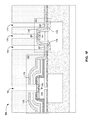
- an integrated photonic semiconductor structure 100 is illustrated.
- the integrated photonic semiconductor structure 100 may include a photonic device such as a Germanium (GE) photodetector 102 and a CMOS device such as an FET transistor 104 .
- the integrated photonic semiconductor structure 100 may further include an optical waveguide structure 106 , a buried oxide (BOX) region 108 , a shallow trench isolation (STI) region 110 , and silicon substrate 112 .
- the BOX region 108 is located over the silicon substrate 112 .
- the optical waveguide structure 106 may be formed within the BOX region 108 in order to facilitate optical confinement and low-loss waveguiding.
- the STI region 110 may provide electrical isolation between the Germanium (Ge) photodetector 102 and the FET transistor 104 .
- the Germanium (Ge) photodetector 102 may include a Ge active region 114 for receiving and detecting an optical signal from optical waveguide structure 106 .
- the optical signal traversing within the optical waveguide structure 106 may be received by the active region 114 through a thin oxide layer 116 and a thin nitride layer 118 .
- any received optical signal received by the active region 114 is attenuated by thin layers 116 and 118 , based on the thickness of these layers 116 , 118 , the attenuation is low enough in order to not impede the operation and sensitivity of the photodetector.
- thin oxide layer 116 may be about 50 ⁇ and thin nitride layer 118 may be about 400 ⁇ .
- the thin oxide layer 116 and thin nitride layer 118 may create a dielectric stack structure 115 that encapsulates the Ge active region 114 of the photodetector 102 .
- the dielectric stack structure 115 which may include oxide layers 116 and 120 , and nitride layers 118 and 122 - 126 , encapsulates the Ge active region 114 during the crystallization process of the Ge active region 114 in order to prevent crystalline defects and contamination as a result of outdiffusion that may occur during high-temperature processes (e.g., epitaxial growth).
- the oxide and nitride layer of the dielectric stack structure 115 may each have thicknesses that vary from, for example, about 1000-3000 Angstroms ( ⁇ ). Also, each of the nitride and oxide layers may include different stress characteristics (e.g., compressive or tensile characteristics).
- a barrier nitride layer 128 such as silicon nitride (Si 3 N 4 ), may be deposited over nitride layer 126 of the dielectric stack 115 . The barrier nitride (Si 3 N 4 ) may be used as an etch stop during subsequent process steps (e.g., see FIG. 1C ).
- a photo resist layer 130 (e.g., thickness ⁇ 8000 ⁇ ) may be patterned in order to allow an opening 132 to be etched (e.g., using a dry etch such as a reactive ion etch) into the dielectric stack structure 115 . Accordingly, the etch process etches down to the upper surface 136 of the Ge active region 114 by etching through barrier nitride layer 128 , nitride layers 122 - 126 , oxide layer 120 , and hard mask layer 134 . As illustrated, a portion P of the Ge active region 114 is now exposed for facilitating the Schottky contact integration process.
- Opening 132 may have a depth (d) of about 3000 ⁇ , as measured with respect to barrier nitride layer 128 , and a diameter/width (D) of approximately 0.15-0.25 ⁇ m. define length (d) from top of layer 128 .
- integrated photonic semiconductor structure 135 is formed by removing photo resist layer 130 ( FIG. 1A ) from integrated photonic semiconductor structure 100 ( FIG. 1A ).
- a metal layer 140 may then be deposited over the entire integrated photonic semiconductor structure 135 . As illustrated, the metal layer 140 also fills opening 132 (also see FIG. 1A ).
- the metal layer 140 may include, for example, titanium nitride (TiN), tantalum nitride (TaN), pulse nucleation layer tungsten (W PNL), and physical vapor deposition tungsten (W PVD).
- the metal layer 140 is selected to be a material that does not intermix with the Ge active region 114 during subsequent process steps (e.g., thermal anneals).
- the surface of the Ge active region 114 may be modified by a barrier tailor implant.
- a barrier tailor implant process is self-aligned with the walls 142 of the dielectric stack structure 115 created by opening 132 .
- n-type dopants such as phosphorous (P), nitrogen (N), arsenic (As), antimony (Sb), or sulfur (S) may be implanted into the surface of the Ge active region 114 in order to increase the barrier height for holes and reduce dark current.
- p-type dopants such as boron (B) or indium (In) may be implanted into the surface of the Ge active region 114 in order to increase the barrier height for electrons, also reducing dark current.
- integrated photonic semiconductor structure 145 may be formed by blanket etching integrated photonic semiconductor structure 135 ( FIG. 1B ). As illustrated, barrier nitride layer 128 acts as an etch stop during the etching of the metal layer 140 ( FIG. 1B ). Thus, metal contact layer 148 may be formed by etching away the metal layer 140 ( FIG. 1B ) from the surface of the integrated photonic semiconductor structure 145 and part of the metal layer deposited within the opening 132 . The metal contact layer 148 directly contacts the portion P of the Ge active region 114 that is exposed by the opening 132 to form a metal-germanium (Ge) Schottky contact 148 .
- Ge germanium
- n-type or p-type dopants may (optionally) be implanted into the surface of the Ge active region 114 , as defined at region 150 , in order to reduce dark current for the metal-Ge Schottky contact 148 .
- the metal-Ge Schottky contact 148 may have a thickness of about 1000 ⁇ .
- integrated photonic semiconductor structure 160 is formed by depositing an oxide or a nitride liner 162 over integrated photonic semiconductor structure 145 ( FIG. 1C ). As illustrated, the oxide or nitride liner 162 is deposited over barrier nitride layer 128 , the metal-germanium (Ge) Schottky contact 148 , and the walls 142 ( FIG. 1B ) of opening 132 .
- oxide or nitride liner 162 is deposited over barrier nitride layer 128 , the metal-germanium (Ge) Schottky contact 148 , and the walls 142 ( FIG. 1B ) of opening 132 .
- integrated photonic semiconductor structure 155 may be formed by depositing a thick oxide layer (e.g., 1 ⁇ m thickness) of borophosphosilicate glass (BPSG) 156 over integrated photonic semiconductor structure 145 ( FIG. 1C ) and planarizing the BPSG layer 156 using, for example, chemical mechanical polishing (CMP).
- the BPSG layer 156 may be used in subsequent contact formation steps corresponding to both the Germanium (GE) photodetector 102 and the FET transistor 104 .
- integrated photonic semiconductor structure 155 may be formed by depositing the thick oxide layer of borophosphosilicate glass (BPSG) 156 over integrated photonic semiconductor structure 160 ( FIG. 1D ).
- the thick oxide layer of borophosphosilicate glass (BPSG) 156 may be formed over the optionally deposited oxide or nitride liner 162 .
- the optional oxide or nitride liner 162 may act as an etch stop when etching through the BPSG layer 156 down to the metal-germanium (Ge) Schottky contact 148 and the gate silicide contact 164 of the FET transistor 104 .
- the etch stop provided by the oxide or nitride liner 162 establishes a means of avoiding the over-etching of both the gate silicide contact 164 and the metal-germanium (Ge) Schottky contact 148 during the BPSG layer 156 etch phase.
- One or more subsequent etches may then be carried out to provide an opening (not shown) in the oxide or nitride liner 162 and the barrier nitride layer 128 down to the upper surface of the gate silicide contact 164 , as defined by surface A.
- the one or more subsequent etches may also provide an opening (not shown) in the oxide or nitride liner 162 down to the upper surface of the metal-germanium (Ge) Schottky contact 148 , as defined by surface B.
- oxide or nitride liner 162 may include either a deposited oxide liner or a nitride liner, by utilizing a nitride type liner (e.g., Si 3 N 4 ) material, a single nitride etch process step may be used to create an opening down to surfaces A and B of gate silicide contact 164 and metal-germanium (Ge) Schottky contact 148 , respectively.
- a nitride type liner e.g., Si 3 N 4
- the deposition of the oxide or nitride liner 162 may protect the underlying metal-germanium (Ge) Schottky contact 148 based on the possible occurrence of voiding during the filling of the opening 132 with BPSG layer 156 .
- the absence of the oxide or nitride liner 162 may permit the etch process to attack the underlying metal-germanium (Ge) Schottky contact 148 .
- the oxide or nitride liner 162 may act as a barrier in the event that the voiding in the opening 132 exposes metal-germanium (Ge) Schottky contact 148 to the etch process (e.g., etch gases).
- the etch process attacks the oxide or nitride liner 162 rather than the metal-germanium (Ge) Schottky contact 148 .
- integrated photonic semiconductor structure 165 may be formed by photolithographic patterning and etching of integrated photonic semiconductor structure 155 ( FIG. 1E ). Particularly, the BPSG layer 156 ( FIG. 1E ) may be patterned, within the same mask, and etched to create contact holes 166 - 172 . The contact holes 166 - 172 enable the formation of an electrical contact to both the Germanium (Ge) photodetector 102 and the FET transistor 104 devices.
- contact hole 166 facilitates the creation of an electrical contact to the metal-germanium (Ge) Schottky contact 148 of the Germanium (Ge) photodetector 102
- contact hole 170 facilitates the creation of an electrical contact to the gate silicide contact 164 of FET transistor 104
- contact holes 168 and 172 enable the forming of electrical contacts to source/drain silicide contacts 176 and 178 of FET transistor 104 , respectively.
- contact hole 166 is formed within opening 132 and is, therefore, of a smaller diameter than the opening 132 .
- the optional oxide or nitride liner 162 may be omitted. Therefore, the etching of the contact holes 168 - 172 that corresponds to the FET transistor 104 stops on the barrier nitride layer 128 , as defined at surfaces S 1 -S 3 . Since the metal-germanium (Ge) Schottky contact 148 is not covered by an etch stop layer such as barrier nitride layer 128 , the etching process may be stopped on the surface B of the metal-germanium (Ge) Schottky contact 148 in order to avoid the over-etching of the metal material forming the contact 148 .
- etch residue associated with the BPSG layer 156 may be removed using POR (process-of-record) post-etch cleaning methods using chemicals such as, for example, hydrogen peroxide (H 2 O 2 ), ammonium hydroxide (NH 4 OH), hydrochloric acid (HCL), and hydrofluoric acid (HF). Since the above-mentioned residue-cleaning chemistry can etch away the germanium material of the Ge active region 114 , the metal-germanium (Ge) Schottky contact 148 may act as a plug that seals the underlying Ge active region 114 from exposure to such residue-cleaning chemistry. Thus, the metal-germanium (Ge) Schottky contact 148 facilitates the cleaning process by protecting the Ge active region 114 from damage caused by the cleaning chemicals.
- POR process-of-record
- integrated photonic semiconductor structure 175 may be formed by a second etch of integrated photonic semiconductor structure 165 ( FIG. 1F ). Accordingly, during a subsequent etch, the barrier nitride layer 128 over surfaces S 1 -S 3 ( FIG. 1F ) is etched away in order to extend the contact holes 168 - 172 down to surfaces S 1 ′-S 3 ′ of silicide contacts 176 , 164 , and 178 , respectively. Also, as depicted at 180 , during the etching of the barrier nitride layer 128 located over surfaces S 1 -S 3 ( FIG.
- a portion of the metal-germanium (Ge) Schottky contact 148 may also be etched away.
- a low metal etch rate may be used.
- etch residue may be removed using POR (process-of-record) post-etch cleaning methods using chemicals such as, for example, hydrogen peroxide (H 2 O 2 ), ammonium hydroxide (NH 4 OH), hydrochloric acid (HCL), and hydrofluoric acid (HF).
- H 2 O 2 hydrogen peroxide
- NH 4 OH ammonium hydroxide
- HCL hydrochloric acid
- HF hydrofluoric acid
- the above-mentioned residue-cleaning chemistry can etch away the germanium material of the Ge active region 114 .
- the metal-germanium (Ge) Schottky contact 148 may seal and, therefore, protect the underlying Ge active region 114 from exposure to such residue-cleaning processes.
- integrated photonic semiconductor structure 185 may be formed by depositing a first metal liner 187 over the sidewalls and floor of the contact holes 168 - 172 of integrated photonic semiconductor structure 175 ( FIG. 1G ).
- the first metal liner 187 may, for example, include a layer of titanium (Ti).
- integrated photonic semiconductor structure 190 may be formed by depositing a second liner 192 over first metal liner 187 within contact holes 168 - 172 .
- the second liner 192 may, for example, include a layer of titanium nitride (TiN).
- TiN liner 192 is deposited over the Ti metal liner 187 , a thermal anneal is carried out in order to cause the deposited Ti/TiN liners 187 , 192 to metallically intermix with the cobalt silicide (CoSi 2 ) contacts 164 , 176 , 178 of the CMOS FET transistor 104 .
- CoSi 2 cobalt silicide
- This intermixing provides a lower Ohmic contact resistance between the deposited Ti/TiN liners 187 , 192 and the cobalt silicide (CoSi 2 ) contacts 164 , 176 , 178 of the CMOS FET device 104 .
- a tungsten metal fill 194 is deposited over TiN liner 192 within the contact holes 168 - 172 . Any excess tungsten associated with the fill process is planarized down to the upper surface D of the BPSG layer 156 .
- the thermal anneal process which provides a reduction in Ohmic contact resistance for the silicide (CoSi 2 ) contacts 164 , 176 , 178 of the CMOS FET device 104 , undesirable intermixing between the material of the deposited Ti/TiN liners 187 , 192 and the Ge active region 114 is avoided based on the intermediary of the metal-germanium (Ge) Schottky contact 148 that isolates the Ti/TiN liners 187 , 192 from the Ge active region 114 .
- the metal-germanium (Ge) Schottky contact 148 material does not intermix with the Ge active region 114 causing undesirable excess dark current.
- the increased barrier height of the metal-germanium (Ge) Schottky contact 148 created by barrier tailor implants within region 150 of the Ge active region 114 may further reduce dark current. While the thermal anneal causing metal intermixing is a beneficial process with respect to the CMOS FET device, any resulting metal intermixing may be detrimental to the photodetector 102 as a result of causing an increase in dark current. Accordingly, the described exemplary embodiment provides a means of maintaining the integrity of both the CMOS (e.g., FET: 104 ) and photonic (e.g., photodetector: 102 ) devices during the contact integration process, whereby electrical contacts are created for both devices 102 , 104 .
- CMOS e.g., FET: 104
- photonic e.g., photodetector: 102
- contact holes 168 - 172 may be substantially circular, as indicated at 196 .
- contact holes 168 - 172 may be substantially rectangular for forming a contact bar, as indicated at 198 .
- FIGS. 2A-2E are vertical cross-sectional views of an integrated photonic semiconductor device structure during Schottky contact integration according to another exemplary embodiment.
- an integrated photonic semiconductor structure 200 is illustrated.
- the integrated photonic semiconductor structure 200 is substantially identical to that of FIG. 1A .
- the integrated photonic semiconductor structure 200 may include a photonic device such as a Germanium (GE) photodetector 202 and a CMOS device such as an FET transistor 204 .
- the integrated photonic semiconductor structure 200 may further include an optical waveguide structure 206 , a buried oxide (BOX) region 208 , a shallow trench isolation (STI) region 210 , and silicon substrate 212 .
- BOX buried oxide
- STI shallow trench isolation
- the BOX region 208 is located over the silicon substrate 212 .
- the optical waveguide structure 206 may be formed within the BOX region 208 in order to facilitate optical confinement and low-loss waveguiding.
- the STI region 210 may provide electrical isolation between the Germanium (Ge) photodetector 202 and the FET transistor 204 .
- the Germanium (Ge) photodetector 202 may include a Ge active region 214 for receiving and detecting an optical signal from optical waveguide structure 206 .
- the optical signal traversing within the optical waveguide structure 206 may be received by the active region 214 through a thin oxide layer 216 and a thin nitride layer 218 .
- any received optical signal received by the active region 214 is attenuated by thin layers 216 and 218 , this attenuation is low enough in order to not impede the operation of the photodetector.
- thin oxide layer 216 may be about 50 ⁇ and thin nitride layer 218 may be about 400 ⁇ .
- the thin oxide layer 216 and thin nitride layer 218 may create a dielectric stack structure 215 that encapsulates the Ge active region 214 of the photodetector 202 .
- the dielectric stack structure 215 which may include oxide layers 216 and 220 , and nitride layers 218 and 222 - 226 , encapsulates the Ge active region 214 during the crystallization process of the Ge active region 214 in order to prevent crystalline defects and contamination as a result of outdiffusion that may occur during high-temperature processes (e.g., epitaxial growth).
- the oxide and nitride layer of the dielectric stack structure 215 may have thicknesses that vary from, for example, about 1000-3000 ⁇ . Also, each of the nitride and oxide layers may include different stress characteristics (e.g., compressive or tensile characteristics).
- a barrier nitride layer 228 such as silicon nitride (Si 3 N 4 ), may be deposited over nitride layer 226 of the dielectric stack 215 . The barrier nitride (Si 3 N 4 ) may be used as an etch stop during subsequent process steps (e.g., see FIG. 2B ).
- opening 232 is etched (e.g., using a dry etch such as a reactive ion etch) into the dielectric stack structure 215 . Accordingly, the etch process etches down to the upper surface 236 of the Ge active region 214 by etching through barrier nitride layer 228 , nitride layers 222 - 126 , oxide layer 220 , and hard mask layer 234 . As illustrated, a portion P of the Ge active region 214 is now exposed for facilitating the Schottky contact integration process. Opening 232 may have a depth of about 3000 ⁇ and a diameter/width of approximately 0.15-0.25 ⁇ m.
- a metal layer 240 may then be deposited over the entire integrated photonic semiconductor structure 200 . As illustrated, the metal layer 140 also lines the walls and floor of opening 232 .
- the metal layer 240 may include, for example, a titanium nitride (TiN), tantalum nitride (TaN), pulse nucleation layer tungsten (W PNL), and physical vapor deposition tungsten (W PVD) material.
- TiN titanium nitride
- TaN tantalum nitride
- W PNL pulse nucleation layer tungsten
- W PVD physical vapor deposition tungsten
- the surface of the Ge active region 214 may be modified by a barrier tailor implant.
- a barrier tailor implant process is self-aligned with the walls of the dielectric stack structure 215 created by opening 232 .
- n-type dopants such as phosphorous (P), nitrogen (N), arsenic (As), antimony (Sb), or sulfur (S) may be implanted into the surface of the Ge active region 214 in order to increase the barrier height for holes and reduce dark current.
- p-type dopants such as boron (B) or indium (In) may be implanted into the surface of the Ge active region 214 in order to increase the barrier height for electrons, also reducing dark current.
- integrated photonic semiconductor structure 235 may be formed by photolithographically patterning and etching integrated photonic semiconductor structure 200 ( FIG. 2A ). As illustrated, metal layer portion 242 is protected by patterned photo resist layer 244 during a subsequent etch of the remaining portion of the metal liner 240 , as indicated by dotted region 246 . The barrier nitride layer 228 may act as an etch stop during the etching of the remaining portion of the metal layer designated by dotted region 246 . Thus, metal layer portion 242 may be formed by etching away metal region 246 from the surface of the integrated photonic semiconductor structure 235 . The metal layer portion 242 directly contacts portion P of the Ge active region 114 that is exposed by the opening 232 ( FIG.
- the metal-germanium (Ge) Schottky landing contact 242 may include landing contacts C 1 and C 2 , as well liner W, which lines the walls and floor of opening 232 ( FIG. 2A ).
- n-type or p-type dopants may (optionally) be implanted into the surface of the Ge active region 214 , as defined at region 250 , in order to reduce dark current for the metal-Ge Schottky landing contact 242 .
- integrated photonic semiconductor structure 255 may be formed by depositing a thick oxide layer (e.g., 1 ⁇ m thickness) of borophosphosilicate glass (BPSG) 256 over integrated photonic semiconductor structure 235 ( FIG. 2B ) and planarizing the BPSG layer 256 using, for example, chemical mechanical polishing (CMP).
- BPSG borophosphosilicate glass
- CMP chemical mechanical polishing
- integrated photonic semiconductor structure 265 may be formed by photolithographic patterning and etching of integrated photonic semiconductor structure 255 ( FIG. 2C ). Particularly, the BPSG layer 256 ( FIG. 2C ) may be patterned, within the same mask, and etched to created contact holes 266 - 272 .
- the contact holes 266 - 272 establish the forming of electrical contact to both the Germanium (Ge) photodetector 202 and the FET transistor 204 devices. As depicted, contact hole 266 facilitates the creation of an electrical contact to landing contact C 1 of the metal-germanium (Ge) Schottky landing contact 242 .
- a contact hole (not shown) may be created for providing an electrical contact to landing contact C 2 of the metal-germanium (Ge) Schottky landing contact 242 .
- contact hole 270 facilitates the creation of an electrical contact to the gate silicide contact 264 of FET transistor 204
- contact holes 268 and 272 enable the formation of electrical contacts to source/drain silicide contacts 276 and 278 of FET transistor 204 , respectively.
- contact hole 266 does not have to be aligned with opening 232 , as with the previously described exemplary embodiment of FIG. 1F .
- landing contact C 1 or C 2 provide an increased etch misalignment tolerance, since a contact hole can be formed anywhere along length L 1 of landing contact C 1 or length L 2 of landing contact C 2 .
- the barrier nitride layer 228 covering the FET transistor 204 acts as an etch stop, which impedes the contact holes 276 - 278 from extending down beyond surfaces S 4 -S 6 . Accordingly, during a subsequent etch process (not shown), the barrier nitride layer 228 over surfaces S 4 -S 6 is etched away (see FIG. 2E ) in order to extend contact holes 268 , 270 , and 272 down to surfaces S 4 ′-S 6 ′ of silicide contacts 276 , 264 , and 278 , respectively.
- integrated photonic semiconductor structure 285 may be formed by depositing a first metal liner 292 over the sidewalls and floor of contact holes 266 - 272 of integrated photonic semiconductor structure 265 ( FIG. 2D ).
- the first metal liner 292 may, for example, include a layer of titanium (Ti).
- a second liner 287 may be deposited over first metal liner 292 within contact holes 266 - 272 .
- the second liner 287 may, for example, include a layer of titanium nitride (TiN).
- a thermal anneal is carried out in order cause the deposited Ti/TiN liners 287 , 292 to metallically intermix with the cobalt silicide (CoSi 2 ) contacts 264 , 276 , 278 of the CMOS FET transistor 204 .
- This intermixing provides a lower Ohmic contact resistance between the deposited Ti/TiN liners 287 , 292 and the cobalt silicide (CoSi 2 ) contacts 264 , 276 , 278 of the CMOS FET device 204 .
- a tungsten metal fill 294 is deposited over the TiN liner 287 within the contact holes 266 - 272 . Any excess tungsten associated with the fill process is planarized down to the upper surface D′ of the BPSG layer 256 .
- the increased barrier height of the metal-germanium (Ge) Schottky landing contact 242 created by barrier tailor implants within region 250 of the Ge active region 214 may further reduce dark current by unpinning the Fermi level within the active region 214 .
- the thermal anneal process causing metal intermixing is a beneficial process with respect to the CMOS FET device 204 ; any resulting metal intermixing may be detrimental to the photodetector 202 as a result of causing an increase in dark current.
- the reduction in dark current may be at least two-fold. Firstly, the barrier tailor implanting may shift the Fermi level and increase the barrier height for electrons or holes. Secondly, less metal intermixing may reduce dangling bonds which reduce electrons from midgap states from contributing to the dark current.
- FIGS. 3A-3F are vertical cross-sectional views of an integrated photonic semiconductor structure during Schottky contact integration according to yet another exemplary embodiment.
- the integrated photonic semiconductor structure 305 may include a photonic device such as a Germanium (GE) photodetector 301 and a CMOS device such as an FET transistor 303 .
- the integrated photonic semiconductor structure 305 may further include an optical waveguide structure 307 , a buried oxide (BOX) region 309 , a shallow trench isolation (STI) region 311 , and silicon substrate 313 .
- the BOX region 309 is located over the silicon substrate 313 .
- the optical waveguide structure 307 may be formed within the BOX region 309 in order to facilitate optical confinement and low-loss waveguiding.
- the STI region 311 may provide electrical isolation between the Germanium (Ge) photodetector 301 and the FET transistor 303 .
- the Germanium (Ge) photodetector 301 may include a Ge active region 306 for receiving and detecting an optical signal from optical waveguide structure 307 .
- the optical signal traversing within the optical waveguide structure 307 may be received by the active region 306 through a thin oxide layer 316 and a thin nitride layer 318 .
- any received optical signal received by the active region 306 is attenuated by thin layers 316 and 318 , this attenuation is low enough in order to not impede the operation of the photodetector.
- thin oxide layer 316 may be about 50 ⁇ and thin nitride layer 318 may be about 400 ⁇ .
- the thin oxide layer 316 and thin nitride layer 318 may create a dielectric stack structure 315 that encapsulates the Ge active region 306 of the photodetector 301 .
- the dielectric stack structure 315 which may include oxide layers 316 and 320 , and nitride layers 318 and 322 - 326 , encapsulates the Ge active region 306 during the crystallization process of the Ge active region 306 in order to prevent crystalline defects and contamination as a result of outdiffusion that may occur during high-temperature processes (e.g., epitaxial growth).
- the oxide and nitride layer of the dielectric stack structure 315 may each have thicknesses that vary from, for example, about 1000-3000 ⁇ . Also, each of the nitride and oxide layers may include different stress characteristics (e.g., compressive or tensile characteristics).
- a barrier nitride layer 328 such as silicon nitride (Si 3 N 4 ), may be deposited over nitride layer 326 of the dielectric stack 315 .
- integrated photonic semiconductor structure 305 may include metal contact layer 302 , which directly contacts portion P of the Ge active region 306 to form a metal-germanium (Ge) Schottky contact 302 within opening 310 .
- Opening 310 may have a depth of about 3000 ⁇ and a diameter/width of approximately 0.15-0.25 ⁇ m.
- n-type or p-type dopants may (optionally) be implanted into the surface of the Ge active region 306 , as defined at region 312 .
- the implants in the surface of the Ge active region 306 may reduce dark current.
- Such a barrier tailor implant process is self-aligned with the walls 342 of the dielectric stack structure 315 created by opening 310 .
- n-type dopants such as phosphorous (P), nitrogen (N), arsenic (As), antimony (Sb), or sulfur (S) may be implanted into the surface of the Ge active region 306 in order to increase the barrier height for holes and reduce dark current.
- p-type dopants such as boron (B) or indium (In) may be implanted into the surface of the Ge active region 306 in order to increase the barrier height for electrons, also reducing dark current.
- a layer of BPSG 330 (e.g., 1 ⁇ m thickness) is deposited over integrated photonic semiconductor structure 305 .
- the layer of BPSG 330 is etched using patterned photoresist layer 334 .
- a second opening 320 is created in the dielectric stack structure 315 .
- the etch process etches down to upper surface 336 of the Ge active region 306 by etching through barrier nitride layer 328 , nitride layers 322 - 326 , oxide layer 320 , and hard mask layer 335 .
- a portion P′ of the Ge active region 306 is now exposed for facilitating a second metal-Ge Schottky contact in addition to metal-Ge Schottky contact 302 .
- the patterned photoresist layer 334 ( FIG. 3A ) is stripped.
- a second metal layer 350 having a different metal work function to that of the metal used to form metal-Ge Schottky contact 302 is deposited within the second opening 320 and over the upper surface (D′′) of the layer of BPSG 330 .
- Both the deposited second metal 350 and the metal used in the formation of the metal-Ge Schottky contact 302 may include, for example, titanium nitride (TiN), tantalum nitride (TaN), pulse nucleation layer tungsten (W PNL), and physical vapor deposition tungsten (W PVD).
- TiN titanium nitride
- TaN tantalum nitride
- W PNL pulse nucleation layer tungsten
- W PVD physical vapor deposition tungsten
- the titanium nitride (TiN), tantalum nitride (TaN), pulse nucleation layer tungsten (W PNL), and physical vapor deposition tungsten (W PVD) are utilized because they do not intermix with the Ge active region 306 during subsequent process steps (e.g., thermal anneals).
- n-type or p-type dopants may (optionally) be implanted into the surface of the Ge active region 306 , as defined at region 355 .
- the implants in the surface region 355 of the Ge active region 306 may reduce dark current.
- Such a barrier tailor implant process is self-aligned with the walls 357 of the dielectric stack structure 315 created by opening 320 .
- n-type dopants such as phosphorous (P), nitrogen (N), arsenic (As), antimony (Sb), or sulfur (S) may be implanted into the surface region 355 of the Ge active region 306 in order to increase the barrier height for holes and reduce dark current.
- p-type dopants such as boron (B) or indium (In) may be implanted into the surface region 355 of the Ge active region 306 in order to increase the barrier height for electrons, also reducing dark current.
- the barrier height between the Ge active region 306 and a direct metallic contact forming a Schottky contact may be determined by both the work function of the metal material corresponding to the metal contact and the implant type (e.g., n-type or p-type) applied to the Ge active region 306 .
- metal-Ge Schottky contact 302 and implant region 312 may provide an increased barrier height for electrons, whereby p-type dopants such as boron (B) or indium (In) may be implanted.
- the second metal 350 in contact with implant region 355 of the Ge active region 306 may provide an increased barrier height for holes, whereby n-type dopants such as phosphorous (P), nitrogen (N), arsenic (As), antimony (Sb), or sulfur (S) may be implanted.
- metal-Ge Schottky contact 302 and implant region 312 may provide an increased barrier height for holes, whereby n-type dopants such as phosphorous (P), nitrogen (N), arsenic (As), antimony (Sb), or sulfur (S) may be implanted.
- n-type dopants such as phosphorous (P), nitrogen (N), arsenic (As), antimony (Sb), or sulfur (S) may be implanted.
- the second metal 350 in contact with implant region 355 of the Ge active region 306 may provide an increased barrier height for electrons, whereby p-type dopants such as boron (B) or indium (In) may be implanted.
- the barrier height for both holes and electrons associated with the Schottky contact regions are optimized to minimize dark current produced by the Ge active region 306 for the photodetector 301 .
- integrated photonic semiconductor structure 360 may be formed by blanket etching the deposited second metal 350 ( FIG. 3B ) associated with integrated photonic semiconductor structure 345 ( FIG. 3B ).
- the deposited second metal 350 FIG. 3B
- the second metal-Ge Schottky contact may be formed to substantially have the same physical dimension as metal-Ge Schottky contact 302 .
- the second metal-Ge Schottky contact 365 is larger than the metal-Ge Schottky contact 302 .
- the formation of the larger metal-Ge Schottky contact 365 may, for example, compensate for different etch rates, whereby the second metal-Ge Schottky contact 365 may be etched at a faster rate than that of metal-Ge Schottky contact 302 based on the use of different metallic materials. Moreover, the formation of the larger metal-Ge Schottky contact 365 may, for example, require less liner and metal fill deposition during contact integration (see FIG. 3F ) in comparison to metal-Ge Schottky contact 302 and silicide contacts 340 , 342 , and 344 , which may require deeper contact holes.
- integrated photonic semiconductor structure 370 may be formed by depositing, patterning, and etching photoresist layer 372 in order to produce contact holes in integrated photonic semiconductor structure 360 ( FIG. 3C ).
- contact hole 374 is etched into the BPSG material within opening 310 ( FIG. 3C ) in order to facilitate the establishment of an electrical connection with metal-Ge Schottky contact 302 .
- contact holes 376 - 380 are produced by etching into a region of the BPSG material 330 ( FIG. 3C ) located over the FET transistor 303 in order to form electrical connectivity with the respective silicide contacts 342 , 340 , 344 of transistor 303 .
- integrated photonic semiconductor structure 380 may be formed by removing the patterned and etched photoresist layer 372 ( FIG. 3D ) of integrated photonic semiconductor structure 370 ( FIG. 3D ), and subsequently forming electrical connections with metal-Ge Schottky contact 302 , metal-Ge Schottky contact 365 , and silicide contacts 340 - 344 . Accordingly, a first metal liner 392 is deposited over the sidewalls and floor of contact holes 376 - 382 of the integrated photonic semiconductor structure 380 . As depicted, contact hole 382 is formed by removing the photoresist material (see FIG. 3D ) covering metal-Ge Schottky contact 365 .
- the first metal liner 392 may, for example, include a layer of titanium (Ti).
- a second liner 387 may be deposited over first metal liner 392 within contact holes 376 - 382 .
- the second liner 387 may, for example, include a layer of titanium nitride (TiN).
- a thermal anneal is carried out in order to cause the deposited Ti/TiN liners 287 , 292 to metallically intermix with the cobalt silicide (CoSi 2 ) contacts 342 , 340 , 344 of the CMOS FET transistor 301 .
- This intermixing provides a lower Ohmic contact resistance between the deposited Ti/TiN liners 387 , 392 and the cobalt silicide (CoSi 2 ) contacts 342 , 340 , 344 of the CMOS FET device 301 .
- a tungsten metal fill 394 is deposited over the TiN liner 387 within the contact holes 376 - 382 . Any excess tungsten associated with the fill process may be planarized down to the upper surface D′′ of the BPSG layer 330 .
- the thermal anneal process which provides a reduction in Ohmic contact resistance for the silicide (CoSi 2 ) contacts 342 , 340 , 344 , undesirable intermixing between the material of the deposited Ti/TiN liners 387 , 392 and the Ge active region 306 is avoided via the intermediary of metal-Ge Schottky contacts 302 and 365 .
- This is based on the metal-Ge Schottky contacts 302 and 365 isolating the Ti/TiN liners 387 , 392 from the Ge active region 306 . Therefore, the Ti/TiN liners 387 , 392 may not undesirably intermix with the Ge active region 306 .
- the metal-Ge Schottky contacts 302 , 365 materials do not intermix with the Ge active region 306 causing undesirable excess dark current.
- the increased barrier height of the metal-Ge Schottky contacts 302 , 365 created by barrier tailor implants within respective regions 312 and 355 of the Ge active region 306 may further reduce dark current by unpinning the Fermi level within the active region 306 .
- the thermal anneal process causing metal intermixing is a beneficial process with respect to the CMOS FET device 303 ; any resulting metal intermixing may be detrimental to the photodetector 301 as a result of causing an increase in dark current.
- the reduction in dark current may be at least two-fold. Firstly, the barrier tailor implanting may shift the Fermi level and increase the barrier height for electrons or holes. Secondly, less metal intermixing may reduce dangling bonds which reduces electrons from midgap states from contributing to the dark current.
- FIG. 4 shows a block diagram of an exemplary design flow 900 used for example, in semiconductor IC logic design, simulation, test, layout, and manufacture.
- Design flow 900 includes processes and mechanisms for processing design structures or devices to generate logically or otherwise functionally equivalent representations of the design structures and/or devices described above and shown in FIGS. 1I , 2 E & 3 E.
- the design structure processed and/or generated by design flow 900 may be encoded on machine-readable transmission or storage media to include data and/or instructions that when executed or otherwise processed on a data processing system generate a logically, structurally, mechanically, or otherwise functionally equivalent representation of hardware components, circuits, devices, or systems.
- Design flow 900 may vary depending on the type of representation being designed. For example, a design flow 900 for building an application specific IC (ASIC) may differ from a design flow 900 for designing a standard component or from a design flow 900 for instantiating the design into a programmable array, for example a programmable gate array (PGA) or a field programmable gate array (FPGA) offered by Altera® Inc. or Xilinx® Inc.
- ASIC application specific IC
- PGA programmable gate array
- FPGA field programmable gate array
- FIG. 4 illustrates multiple such design structures including an input design structure 920 that is preferably processed by a design process 910 .
- the design structure 920 comprises design data used in a design process and comprising information describing one or more embodiments of the invention with respect to the structures as shown in FIGS. 1I , 2 E & 3 E.
- the design data in the form of schematics or HDL, a hardware-description language (e.g., Verilog, VHDL, C, etc.) may be embodied on one or more machine readable media.
- design structure 920 may be a text file, numerical data or a graphical representation of the one or more embodiments of the invention, as shown in FIGS. 11 , 2 E & 3 E.
- Design structure 920 may be a logical simulation design structure generated and processed by design process 910 to produce a logically equivalent functional representation of a hardware device.
- Design structure 920 may also or alternatively comprise data and/or program instructions that when processed by design process 910 , generate a functional representation of the physical structure of a hardware device. Whether representing functional and/or structural design features, design structure 920 may be generated using electronic computer-aided design (ECAD) such as implemented by a core developer/designer.
- ECAD electronic computer-aided design
- design structure 920 When encoded on a machine-readable data transmission, gate array, or storage medium, design structure 920 may be accessed and processed by one or more hardware and/or software modules within design process 910 to simulate or otherwise functionally represent an electronic component, circuit, electronic or logic module, apparatus, device, or system such as those shown in FIGS. 1I , 2 E & 3 E.
- design structure 920 may comprise files or other data structures including human and/or machine-readable source code, compiled structures, and computer-executable code structures that when processed by a design or simulation data processing system, functionally simulate or otherwise represent circuits or other levels of hardware logic design.
- Such data structures may include hardware-description language (HDL) design entities or other data structures conforming to and/or compatible with lower-level HDL design languages such as Verilog and VHDL, and/or higher level design languages such as C or C++.
- HDL hardware-description language
- Design process 910 preferably employs and incorporates hardware and/or software modules for synthesizing, translating, or otherwise processing a design/simulation functional equivalent of the components, circuits, devices, or logic structures shown in FIGS. 1I , 2 E & 3 E to generate a netlist 980 which may contain a design structure such as design structure 920 .
- Netlist 980 may comprise, for example, compiled or otherwise processed data structures representing a list of wires, discrete components, logic gates, control circuits, I/O devices, models, etc. that describes the connections to other elements and circuits in an integrated circuit design.
- Netlist 980 may be synthesized using an iterative process in which netlist 980 is resynthesized one or more times depending on design specifications and parameters for the device.
- netlist 980 may be recorded on a machine-readable data storage medium or programmed into a programmable gate array.
- the medium may be a non-volatile storage medium such as a magnetic or optical disk drive, a programmable gate array, a compact flash, or other flash memory. Additionally, or in the alternative, the medium may be a system or cache memory, buffer space, or electrically or optically conductive devices and materials on which data packets may be transmitted and intermediately stored via the Internet, or other networking suitable means.
- Design process 910 may include hardware and software modules for processing a variety of input data structure types including netlist 980 .
- data structure types may reside, for example, within library elements 930 and include a set of commonly used elements, circuits, and devices, including models, layouts, and symbolic representations, for a given manufacturing technology (e.g., different technology nodes, 20, 32 nm, 45 nm, 90 nm, etc.).
- the data structure types may further include design specifications 940 , characterization data 950 , verification data 960 , design rules 970 , and test data files 985 which may include input test patterns, output test results, and other testing information.
- Design process 910 may further include, for example, standard mechanical design processes such as stress analysis, thermal analysis, mechanical event simulation, process simulation for operations such as casting, molding, and die press forming, etc.
- standard mechanical design processes such as stress analysis, thermal analysis, mechanical event simulation, process simulation for operations such as casting, molding, and die press forming, etc.
- One of ordinary skill in the art of mechanical design can appreciate the extent of possible mechanical design tools and applications used in design process 910 without deviating from the scope and spirit of the invention.
- Design process 910 may also include modules for performing standard circuit design processes such as timing analysis, verification, design rule checking, place and route operations, etc.
- Design process 910 employs and incorporates logic and physical design tools such as HDL compilers and simulation model build tools to process design structure 920 together with some or all of the depicted supporting data structures along with any additional mechanical design or data (if applicable), to generate a second design structure 990 comprising second design data embodied on a storage medium in a data format used for the exchange of layout data of integrated circuits and/or symbolic data format (e.g. information stored in a GDSII (GDS2), GL1, OASIS, map files, or any other suitable format for storing such design structures).
- the second design data resides on a storage medium or programmable gate array in a data format used for the exchange of data of mechanical devices and structures (e.g.
- design structure 990 preferably comprises one or more files, data structures, or other computer-encoded data or instructions that reside on transmission or data storage media and that when processed by an ECAD system generate a logically or otherwise functionally equivalent form of one or more of the embodiments of the invention shown in FIGS. 1I , 2 E & 3 E.
- design structure 990 may comprise a compiled, executable HDL simulation model that functionally simulates the devices shown in FIGS. 1I , 2 E & 3 E.
- Design structure 990 may also employ a data format used for the exchange of layout data of integrated circuits and/or symbolic data format (e.g. information stored in a GDSII (GDS2), GL1, OASIS, map files, or any other suitable format for storing such design data structures).
- GDSII GDS2
- GL1 GL1, OASIS, map files, or any other suitable format for storing such design data structures.
- Design structure 990 may comprise information such as, for example, symbolic data, map files, test data files, design content files, manufacturing data, layout parameters, wires, levels of metal, vias, shapes, data for routing through the manufacturing line, and any other data required by a manufacturer or other designer/developer to produce devices or structures as described above and shown in FIGS. 1I , 2 E & 3 E. Design structure 990 may then proceed to a stage 995 where, for example, design structure 990 : proceeds to tape-out, is released to manufacturing, is released to a mask house, is sent to another design house, is sent back to the customer, etc.
Landscapes
- Engineering & Computer Science (AREA)
- Physics & Mathematics (AREA)
- Power Engineering (AREA)
- Computer Hardware Design (AREA)
- Electromagnetism (AREA)
- General Physics & Mathematics (AREA)
- Condensed Matter Physics & Semiconductors (AREA)
- Microelectronics & Electronic Packaging (AREA)
- Manufacturing & Machinery (AREA)
- Optics & Photonics (AREA)
- Electrodes Of Semiconductors (AREA)
- Solid State Image Pick-Up Elements (AREA)
- Metal-Oxide And Bipolar Metal-Oxide Semiconductor Integrated Circuits (AREA)
- Light Receiving Elements (AREA)
Abstract
Description
Claims (11)
Priority Applications (2)
| Application Number | Priority Date | Filing Date | Title |
|---|---|---|---|
| US13/561,177 US8765502B2 (en) | 2012-07-30 | 2012-07-30 | Germanium photodetector schottky contact for integration with CMOS and Si nanophotonics |
| US14/228,106 US9484367B2 (en) | 2012-07-30 | 2014-03-27 | Germanium photodetector schottky contact for integration with CMOS and Si nanophotonics |
Applications Claiming Priority (1)
| Application Number | Priority Date | Filing Date | Title |
|---|---|---|---|
| US13/561,177 US8765502B2 (en) | 2012-07-30 | 2012-07-30 | Germanium photodetector schottky contact for integration with CMOS and Si nanophotonics |
Related Child Applications (1)
| Application Number | Title | Priority Date | Filing Date |
|---|---|---|---|
| US14/228,106 Division US9484367B2 (en) | 2012-07-30 | 2014-03-27 | Germanium photodetector schottky contact for integration with CMOS and Si nanophotonics |
Publications (2)
| Publication Number | Publication Date |
|---|---|
| US20140027826A1 US20140027826A1 (en) | 2014-01-30 |
| US8765502B2 true US8765502B2 (en) | 2014-07-01 |
Family
ID=49994056
Family Applications (2)
| Application Number | Title | Priority Date | Filing Date |
|---|---|---|---|
| US13/561,177 Active US8765502B2 (en) | 2012-07-30 | 2012-07-30 | Germanium photodetector schottky contact for integration with CMOS and Si nanophotonics |
| US14/228,106 Active 2032-12-23 US9484367B2 (en) | 2012-07-30 | 2014-03-27 | Germanium photodetector schottky contact for integration with CMOS and Si nanophotonics |
Family Applications After (1)
| Application Number | Title | Priority Date | Filing Date |
|---|---|---|---|
| US14/228,106 Active 2032-12-23 US9484367B2 (en) | 2012-07-30 | 2014-03-27 | Germanium photodetector schottky contact for integration with CMOS and Si nanophotonics |
Country Status (1)
| Country | Link |
|---|---|
| US (2) | US8765502B2 (en) |
Cited By (5)
| Publication number | Priority date | Publication date | Assignee | Title |
|---|---|---|---|---|
| US20140209985A1 (en) * | 2012-07-30 | 2014-07-31 | International Business Machines Corporation | GERMANIUM PHOTODETECTOR SCHOTTKY CONTACT FOR INTEGRATION WITH CMOS AND Si NANOPHOTONICS |
| US20150303229A1 (en) * | 2013-08-20 | 2015-10-22 | International Business Machines Corporation | Cmos protection during germanium photodetector processing |
| US9536825B2 (en) | 2014-11-19 | 2017-01-03 | Samsung Electronics Co., Ltd. | Semiconductor device and method for fabricating the same |
| US20210135024A1 (en) * | 2019-10-31 | 2021-05-06 | Taiwan Semiconductor Manufacturing Co., Ltd. | Semiconductor device comprising a photodetector with reduced dark current |
| US20230299217A1 (en) * | 2019-10-31 | 2023-09-21 | Taiwan Semiconductor Manufacturing Company, Ltd. | Semiconductor device comprising a photodetector with reduced dark current |
Families Citing this family (17)
| Publication number | Priority date | Publication date | Assignee | Title |
|---|---|---|---|---|
| US9395491B2 (en) * | 2014-02-05 | 2016-07-19 | Aurrion, Inc. | Shielding regions for photonic integrated circuits |
| US9768330B2 (en) * | 2014-08-25 | 2017-09-19 | Micron Technology, Inc. | Method and optoelectronic structure providing polysilicon photonic devices with different optical properties in different regions |
| US9368653B1 (en) * | 2014-12-23 | 2016-06-14 | International Business Machines Corporation | Silicon photonics integration method and structure |
| US9864138B2 (en) | 2015-01-05 | 2018-01-09 | The Research Foundation For The State University Of New York | Integrated photonics including germanium |
| US9874693B2 (en) | 2015-06-10 | 2018-01-23 | The Research Foundation For The State University Of New York | Method and structure for integrating photonics with CMOs |
| US9356163B1 (en) * | 2015-06-16 | 2016-05-31 | International Business Machines Corporation | Structure and method of integrating waveguides, photodetectors and logic devices |
| JP2018049856A (en) * | 2016-09-20 | 2018-03-29 | ルネサスエレクトロニクス株式会社 | Semiconductor device |
| US10976491B2 (en) | 2016-11-23 | 2021-04-13 | The Research Foundation For The State University Of New York | Photonics interposer optoelectronics |
| US10707121B2 (en) * | 2016-12-31 | 2020-07-07 | Intel Corporatino | Solid state memory device, and manufacturing method thereof |
| US10698156B2 (en) | 2017-04-27 | 2020-06-30 | The Research Foundation For The State University Of New York | Wafer scale bonded active photonics interposer |
| WO2019195441A1 (en) | 2018-04-04 | 2019-10-10 | The Research Foundation For The State University Of New York | Heterogeneous structure on an integrated photonics platform |
| US10816724B2 (en) | 2018-04-05 | 2020-10-27 | The Research Foundation For The State University Of New York | Fabricating photonics structure light signal transmission regions |
| TWI773774B (en) * | 2018-06-14 | 2022-08-11 | 聯華電子股份有限公司 | Semiconductor device and method for forming the same |
| KR102590996B1 (en) | 2018-10-17 | 2023-10-17 | 삼성전자주식회사 | Semiconductor device |
| FR3100377A1 (en) * | 2019-08-30 | 2021-03-05 | Commissariat A L'energie Atomique Et Aux Energies Alternatives | Contact on germanium |
| WO2020256819A2 (en) * | 2019-06-18 | 2020-12-24 | The Research Foundation For The State University Of New York | Fabricating photonics structure conductive pathways |
| DE102021109737A1 (en) * | 2020-05-29 | 2021-12-02 | Taiwan Semiconductor Manufacturing Co. Ltd. | GERMANIUM CONTAINING PHOTODETECTOR AND PROCESS FOR ITS MANUFACTURING |
Citations (7)
| Publication number | Priority date | Publication date | Assignee | Title |
|---|---|---|---|---|
| US6756651B2 (en) | 2001-09-26 | 2004-06-29 | International Business Machines Corporation | CMOS-compatible metal-semiconductor-metal photodetector |
| US7157300B2 (en) | 2004-11-19 | 2007-01-02 | Sharp Laboratories Of America, Inc. | Fabrication of thin film germanium infrared sensor by bonding to silicon wafer |
| US7262117B1 (en) | 2003-06-10 | 2007-08-28 | Luxtera, Inc. | Germanium integrated CMOS wafer and method for manufacturing the same |
| US7566875B2 (en) | 2006-04-13 | 2009-07-28 | Integrated Micro Sensors Inc. | Single-chip monolithic dual-band visible- or solar-blind photodetector |
| US7616904B1 (en) | 2002-06-19 | 2009-11-10 | Luxtera, Inc. | Waveguide photodetector with integrated electronics |
| US20110147870A1 (en) * | 2008-02-15 | 2011-06-23 | Kah Wee Ang | Photodetector with valence-mending adsorbate region and a method of fabrication thereof |
| US20120129302A1 (en) * | 2010-11-22 | 2012-05-24 | International Business Machines Corporation | Fabricating photonics devices fully integrated into a cmos manufacturing process |
Family Cites Families (1)
| Publication number | Priority date | Publication date | Assignee | Title |
|---|---|---|---|---|
| US8765502B2 (en) * | 2012-07-30 | 2014-07-01 | International Business Machines Corporation | Germanium photodetector schottky contact for integration with CMOS and Si nanophotonics |
-
2012
- 2012-07-30 US US13/561,177 patent/US8765502B2/en active Active
-
2014
- 2014-03-27 US US14/228,106 patent/US9484367B2/en active Active
Patent Citations (7)
| Publication number | Priority date | Publication date | Assignee | Title |
|---|---|---|---|---|
| US6756651B2 (en) | 2001-09-26 | 2004-06-29 | International Business Machines Corporation | CMOS-compatible metal-semiconductor-metal photodetector |
| US7616904B1 (en) | 2002-06-19 | 2009-11-10 | Luxtera, Inc. | Waveguide photodetector with integrated electronics |
| US7262117B1 (en) | 2003-06-10 | 2007-08-28 | Luxtera, Inc. | Germanium integrated CMOS wafer and method for manufacturing the same |
| US7157300B2 (en) | 2004-11-19 | 2007-01-02 | Sharp Laboratories Of America, Inc. | Fabrication of thin film germanium infrared sensor by bonding to silicon wafer |
| US7566875B2 (en) | 2006-04-13 | 2009-07-28 | Integrated Micro Sensors Inc. | Single-chip monolithic dual-band visible- or solar-blind photodetector |
| US20110147870A1 (en) * | 2008-02-15 | 2011-06-23 | Kah Wee Ang | Photodetector with valence-mending adsorbate region and a method of fabrication thereof |
| US20120129302A1 (en) * | 2010-11-22 | 2012-05-24 | International Business Machines Corporation | Fabricating photonics devices fully integrated into a cmos manufacturing process |
Non-Patent Citations (1)
| Title |
|---|
| Sridaran et al. "Nanophotonic devices on thin buried oxide Silicon-On-Insulator substrates", Cornell University, Ithaca, NY. Published Feb. 11, 2010, vol. 18, No. 4, pp. 3850-3857. |
Cited By (8)
| Publication number | Priority date | Publication date | Assignee | Title |
|---|---|---|---|---|
| US20140209985A1 (en) * | 2012-07-30 | 2014-07-31 | International Business Machines Corporation | GERMANIUM PHOTODETECTOR SCHOTTKY CONTACT FOR INTEGRATION WITH CMOS AND Si NANOPHOTONICS |
| US9484367B2 (en) * | 2012-07-30 | 2016-11-01 | Globalfoundries Inc. | Germanium photodetector schottky contact for integration with CMOS and Si nanophotonics |
| US20150303229A1 (en) * | 2013-08-20 | 2015-10-22 | International Business Machines Corporation | Cmos protection during germanium photodetector processing |
| US9590001B2 (en) * | 2013-08-20 | 2017-03-07 | Globalfoundries Inc. | CMOS protection during germanium photodetector processing |
| US9536825B2 (en) | 2014-11-19 | 2017-01-03 | Samsung Electronics Co., Ltd. | Semiconductor device and method for fabricating the same |
| US20210135024A1 (en) * | 2019-10-31 | 2021-05-06 | Taiwan Semiconductor Manufacturing Co., Ltd. | Semiconductor device comprising a photodetector with reduced dark current |
| US11749762B2 (en) * | 2019-10-31 | 2023-09-05 | Taiwan Semiconductor Manufacturing Company, Ltd. | Semiconductor device comprising a photodetector with reduced dark current |
| US20230299217A1 (en) * | 2019-10-31 | 2023-09-21 | Taiwan Semiconductor Manufacturing Company, Ltd. | Semiconductor device comprising a photodetector with reduced dark current |
Also Published As
| Publication number | Publication date |
|---|---|
| US20140027826A1 (en) | 2014-01-30 |
| US20140209985A1 (en) | 2014-07-31 |
| US9484367B2 (en) | 2016-11-01 |
Similar Documents
| Publication | Publication Date | Title |
|---|---|---|
| US9484367B2 (en) | Germanium photodetector schottky contact for integration with CMOS and Si nanophotonics | |
| US9087952B2 (en) | Stress engineered multi-layers for integration of CMOS and Si nanophotonics | |
| US10347759B2 (en) | Vertical FET structure | |
| US9036959B2 (en) | Intergrating a silicon photonics photodetector with CMOS devices | |
| CN101779284B (en) | Method to fabricate adjacent silicon fins of differing heights | |
| US9229164B2 (en) | Butt-coupled buried waveguide photodetector | |
| US10002882B2 (en) | Method for manufacturing a high-resistivity semiconductor-on-insulator substrate including an RF circuit overlapping a doped region in the substrate | |
| US9240352B2 (en) | Bulk finFET well contacts with fin pattern uniformity | |
| US10522358B2 (en) | FinFET device and methods of forming same | |
| US20210135025A1 (en) | Method and optoelectronic structure providing polysilicon photonic devices with different optical properties in different regions | |
| US9478642B2 (en) | Semiconductor junction formation | |
| TW202230476A (en) | Method of forming semiconductor structure | |
| US9590001B2 (en) | CMOS protection during germanium photodetector processing | |
| TW201732932A (en) | Semiconductor structure and manufacturing method thereof | |
| US20120261745A1 (en) | Semiconductor switching device employing a quantum dot structure | |
| US7537981B2 (en) | Silicon on insulator device and method of manufacturing the same | |
| US9171971B2 (en) | Encapsulated sensors | |
| US20150035076A1 (en) | Self-Aligned Gate Electrode Diffusion Barriers | |
| US9634004B2 (en) | Forming reliable contacts on tight semiconductor pitch | |
| CN114975230B (en) | Semiconductor device manufacturing method and semiconductor device | |
| CN110571193B (en) | Method for manufacturing single diffusion blocking structure and method for manufacturing semiconductor device | |
| CN109786337B (en) | Semiconductor structure and forming method thereof | |
| CN114664740A (en) | CMOS device and method for fabricating the same | |
| KR19990074726A (en) | Separation layer of semiconductor device and forming method thereof |
Legal Events
| Date | Code | Title | Description |
|---|---|---|---|
| AS | Assignment |
Owner name: INTERNATIONAL BUSINESS MACHINES CORPORATION, NEW Y Free format text: ASSIGNMENT OF ASSIGNORS INTEREST;ASSIGNORS:ASSEFA, SOLOMON;GAMBINO, JEFFREY P.;SHANK, STEVEN M.;SIGNING DATES FROM 20120727 TO 20120730;REEL/FRAME:028670/0476 |
|
| STCF | Information on status: patent grant |
Free format text: PATENTED CASE |
|
| AS | Assignment |
Owner name: GLOBALFOUNDRIES U.S. 2 LLC, NEW YORK Free format text: ASSIGNMENT OF ASSIGNORS INTEREST;ASSIGNOR:INTERNATIONAL BUSINESS MACHINES CORPORATION;REEL/FRAME:036550/0001 Effective date: 20150629 |
|
| AS | Assignment |
Owner name: GLOBALFOUNDRIES INC., CAYMAN ISLANDS Free format text: ASSIGNMENT OF ASSIGNORS INTEREST;ASSIGNORS:GLOBALFOUNDRIES U.S. 2 LLC;GLOBALFOUNDRIES U.S. INC.;REEL/FRAME:036779/0001 Effective date: 20150910 |
|
| MAFP | Maintenance fee payment |
Free format text: PAYMENT OF MAINTENANCE FEE, 4TH YEAR, LARGE ENTITY (ORIGINAL EVENT CODE: M1551) Year of fee payment: 4 |
|
| AS | Assignment |
Owner name: WILMINGTON TRUST, NATIONAL ASSOCIATION, DELAWARE Free format text: SECURITY AGREEMENT;ASSIGNOR:GLOBALFOUNDRIES INC.;REEL/FRAME:049490/0001 Effective date: 20181127 |
|
| AS | Assignment |
Owner name: GLOBALFOUNDRIES U.S. INC., CALIFORNIA Free format text: ASSIGNMENT OF ASSIGNORS INTEREST;ASSIGNOR:GLOBALFOUNDRIES INC.;REEL/FRAME:054633/0001 Effective date: 20201022 |
|
| AS | Assignment |
Owner name: GLOBALFOUNDRIES INC., CAYMAN ISLANDS Free format text: RELEASE BY SECURED PARTY;ASSIGNOR:WILMINGTON TRUST, NATIONAL ASSOCIATION;REEL/FRAME:054636/0001 Effective date: 20201117 |
|
| AS | Assignment |
Owner name: GLOBALFOUNDRIES U.S. INC., NEW YORK Free format text: RELEASE BY SECURED PARTY;ASSIGNOR:WILMINGTON TRUST, NATIONAL ASSOCIATION;REEL/FRAME:056987/0001 Effective date: 20201117 |
|
| MAFP | Maintenance fee payment |
Free format text: PAYMENT OF MAINTENANCE FEE, 8TH YEAR, LARGE ENTITY (ORIGINAL EVENT CODE: M1552); ENTITY STATUS OF PATENT OWNER: LARGE ENTITY Year of fee payment: 8 |