EP4002439A1 - Three dimensional integrated semiconductor architecture and method of manufacturing the same - Google Patents
Three dimensional integrated semiconductor architecture and method of manufacturing the same Download PDFInfo
- Publication number
- EP4002439A1 EP4002439A1 EP21206428.1A EP21206428A EP4002439A1 EP 4002439 A1 EP4002439 A1 EP 4002439A1 EP 21206428 A EP21206428 A EP 21206428A EP 4002439 A1 EP4002439 A1 EP 4002439A1
- Authority
- EP
- European Patent Office
- Prior art keywords
- carrier substrate
- alignment marks
- semiconductor device
- semiconductor
- providing
- Prior art date
- Legal status (The legal status is an assumption and is not a legal conclusion. Google has not performed a legal analysis and makes no representation as to the accuracy of the status listed.)
- Pending
Links
- 239000004065 semiconductor Substances 0.000 title claims abstract description 179
- 238000004519 manufacturing process Methods 0.000 title claims description 18
- 239000000758 substrate Substances 0.000 claims abstract description 143
- 239000010410 layer Substances 0.000 claims description 80
- 238000000034 method Methods 0.000 claims description 34
- 238000005530 etching Methods 0.000 claims description 7
- 229910000577 Silicon-germanium Inorganic materials 0.000 claims description 6
- 239000012790 adhesive layer Substances 0.000 claims description 6
- 229910052710 silicon Inorganic materials 0.000 claims description 5
- 239000010703 silicon Substances 0.000 claims description 5
- LEVVHYCKPQWKOP-UHFFFAOYSA-N [Si].[Ge] Chemical compound [Si].[Ge] LEVVHYCKPQWKOP-UHFFFAOYSA-N 0.000 claims description 3
- 239000012212 insulator Substances 0.000 claims description 3
- 238000005498 polishing Methods 0.000 claims description 2
- 230000010354 integration Effects 0.000 description 13
- 230000008569 process Effects 0.000 description 8
- 239000003550 marker Substances 0.000 description 6
- 230000000052 comparative effect Effects 0.000 description 5
- 238000001514 detection method Methods 0.000 description 5
- 238000001312 dry etching Methods 0.000 description 5
- 229910052581 Si3N4 Inorganic materials 0.000 description 4
- VYPSYNLAJGMNEJ-UHFFFAOYSA-N Silicium dioxide Chemical compound O=[Si]=O VYPSYNLAJGMNEJ-UHFFFAOYSA-N 0.000 description 4
- 229910052594 sapphire Inorganic materials 0.000 description 4
- 239000010980 sapphire Substances 0.000 description 4
- HQVNEWCFYHHQES-UHFFFAOYSA-N silicon nitride Chemical compound N12[Si]34N5[Si]62N3[Si]51N64 HQVNEWCFYHHQES-UHFFFAOYSA-N 0.000 description 4
- 239000002356 single layer Substances 0.000 description 4
- XUIMIQQOPSSXEZ-UHFFFAOYSA-N Silicon Chemical compound [Si] XUIMIQQOPSSXEZ-UHFFFAOYSA-N 0.000 description 3
- RKTYLMNFRDHKIL-UHFFFAOYSA-N copper;5,10,15,20-tetraphenylporphyrin-22,24-diide Chemical compound [Cu+2].C1=CC(C(=C2C=CC([N-]2)=C(C=2C=CC=CC=2)C=2C=CC(N=2)=C(C=2C=CC=CC=2)C2=CC=C3[N-]2)C=2C=CC=CC=2)=NC1=C3C1=CC=CC=C1 RKTYLMNFRDHKIL-UHFFFAOYSA-N 0.000 description 3
- 239000011521 glass Substances 0.000 description 3
- 238000002513 implantation Methods 0.000 description 3
- 239000000463 material Substances 0.000 description 3
- 238000001039 wet etching Methods 0.000 description 3
- 238000004891 communication Methods 0.000 description 2
- 238000010586 diagram Methods 0.000 description 2
- 230000014509 gene expression Effects 0.000 description 2
- 238000001020 plasma etching Methods 0.000 description 2
- 239000000377 silicon dioxide Substances 0.000 description 2
- 229920001621 AMOLED Polymers 0.000 description 1
- 230000008859 change Effects 0.000 description 1
- 238000005516 engineering process Methods 0.000 description 1
- 239000007943 implant Substances 0.000 description 1
- 239000004973 liquid crystal related substance Substances 0.000 description 1
- 239000011159 matrix material Substances 0.000 description 1
- 239000002861 polymer material Substances 0.000 description 1
- 230000009467 reduction Effects 0.000 description 1
- 239000011347 resin Substances 0.000 description 1
- 229920005989 resin Polymers 0.000 description 1
- 235000012239 silicon dioxide Nutrition 0.000 description 1
- 239000007787 solid Substances 0.000 description 1
Images


Classifications
-
- H—ELECTRICITY
- H01—ELECTRIC ELEMENTS
- H01L—SEMICONDUCTOR DEVICES NOT COVERED BY CLASS H10
- H01L23/00—Details of semiconductor or other solid state devices
- H01L23/544—Marks applied to semiconductor devices or parts, e.g. registration marks, alignment structures, wafer maps
-
- H—ELECTRICITY
- H01—ELECTRIC ELEMENTS
- H01L—SEMICONDUCTOR DEVICES NOT COVERED BY CLASS H10
- H01L21/00—Processes or apparatus adapted for the manufacture or treatment of semiconductor or solid state devices or of parts thereof
- H01L21/70—Manufacture or treatment of devices consisting of a plurality of solid state components formed in or on a common substrate or of parts thereof; Manufacture of integrated circuit devices or of parts thereof
- H01L21/77—Manufacture or treatment of devices consisting of a plurality of solid state components or integrated circuits formed in, or on, a common substrate
- H01L21/78—Manufacture or treatment of devices consisting of a plurality of solid state components or integrated circuits formed in, or on, a common substrate with subsequent division of the substrate into plural individual devices
- H01L21/82—Manufacture or treatment of devices consisting of a plurality of solid state components or integrated circuits formed in, or on, a common substrate with subsequent division of the substrate into plural individual devices to produce devices, e.g. integrated circuits, each consisting of a plurality of components
- H01L21/822—Manufacture or treatment of devices consisting of a plurality of solid state components or integrated circuits formed in, or on, a common substrate with subsequent division of the substrate into plural individual devices to produce devices, e.g. integrated circuits, each consisting of a plurality of components the substrate being a semiconductor, using silicon technology
- H01L21/8232—Field-effect technology
- H01L21/8234—MIS technology, i.e. integration processes of field effect transistors of the conductor-insulator-semiconductor type
- H01L21/823475—MIS technology, i.e. integration processes of field effect transistors of the conductor-insulator-semiconductor type interconnection or wiring or contact manufacturing related aspects
-
- G—PHYSICS
- G03—PHOTOGRAPHY; CINEMATOGRAPHY; ANALOGOUS TECHNIQUES USING WAVES OTHER THAN OPTICAL WAVES; ELECTROGRAPHY; HOLOGRAPHY
- G03F—PHOTOMECHANICAL PRODUCTION OF TEXTURED OR PATTERNED SURFACES, e.g. FOR PRINTING, FOR PROCESSING OF SEMICONDUCTOR DEVICES; MATERIALS THEREFOR; ORIGINALS THEREFOR; APPARATUS SPECIALLY ADAPTED THEREFOR
- G03F7/00—Photomechanical, e.g. photolithographic, production of textured or patterned surfaces, e.g. printing surfaces; Materials therefor, e.g. comprising photoresists; Apparatus specially adapted therefor
- G03F7/70—Microphotolithographic exposure; Apparatus therefor
- G03F7/70483—Information management; Active and passive control; Testing; Wafer monitoring, e.g. pattern monitoring
- G03F7/70605—Workpiece metrology
- G03F7/70616—Monitoring the printed patterns
- G03F7/70633—Overlay, i.e. relative alignment between patterns printed by separate exposures in different layers, or in the same layer in multiple exposures or stitching
-
- H—ELECTRICITY
- H01—ELECTRIC ELEMENTS
- H01L—SEMICONDUCTOR DEVICES NOT COVERED BY CLASS H10
- H01L21/00—Processes or apparatus adapted for the manufacture or treatment of semiconductor or solid state devices or of parts thereof
- H01L21/70—Manufacture or treatment of devices consisting of a plurality of solid state components formed in or on a common substrate or of parts thereof; Manufacture of integrated circuit devices or of parts thereof
- H01L21/71—Manufacture of specific parts of devices defined in group H01L21/70
- H01L21/768—Applying interconnections to be used for carrying current between separate components within a device comprising conductors and dielectrics
- H01L21/76898—Applying interconnections to be used for carrying current between separate components within a device comprising conductors and dielectrics formed through a semiconductor substrate
-
- H—ELECTRICITY
- H01—ELECTRIC ELEMENTS
- H01L—SEMICONDUCTOR DEVICES NOT COVERED BY CLASS H10
- H01L23/00—Details of semiconductor or other solid state devices
- H01L23/48—Arrangements for conducting electric current to or from the solid state body in operation, e.g. leads, terminal arrangements ; Selection of materials therefor
- H01L23/481—Internal lead connections, e.g. via connections, feedthrough structures
-
- H—ELECTRICITY
- H01—ELECTRIC ELEMENTS
- H01L—SEMICONDUCTOR DEVICES NOT COVERED BY CLASS H10
- H01L23/00—Details of semiconductor or other solid state devices
- H01L23/52—Arrangements for conducting electric current within the device in operation from one component to another, i.e. interconnections, e.g. wires, lead frames
- H01L23/522—Arrangements for conducting electric current within the device in operation from one component to another, i.e. interconnections, e.g. wires, lead frames including external interconnections consisting of a multilayer structure of conductive and insulating layers inseparably formed on the semiconductor body
- H01L23/528—Geometry or layout of the interconnection structure
- H01L23/5286—Arrangements of power or ground buses
-
- H—ELECTRICITY
- H01—ELECTRIC ELEMENTS
- H01L—SEMICONDUCTOR DEVICES NOT COVERED BY CLASS H10
- H01L23/00—Details of semiconductor or other solid state devices
- H01L23/52—Arrangements for conducting electric current within the device in operation from one component to another, i.e. interconnections, e.g. wires, lead frames
- H01L23/535—Arrangements for conducting electric current within the device in operation from one component to another, i.e. interconnections, e.g. wires, lead frames including internal interconnections, e.g. cross-under constructions
-
- H—ELECTRICITY
- H01—ELECTRIC ELEMENTS
- H01L—SEMICONDUCTOR DEVICES NOT COVERED BY CLASS H10
- H01L24/00—Arrangements for connecting or disconnecting semiconductor or solid-state bodies; Methods or apparatus related thereto
- H01L24/80—Methods for connecting semiconductor or other solid state bodies using means for bonding being attached to, or being formed on, the surface to be connected
- H01L24/83—Methods for connecting semiconductor or other solid state bodies using means for bonding being attached to, or being formed on, the surface to be connected using a layer connector
-
- H—ELECTRICITY
- H01—ELECTRIC ELEMENTS
- H01L—SEMICONDUCTOR DEVICES NOT COVERED BY CLASS H10
- H01L24/00—Arrangements for connecting or disconnecting semiconductor or solid-state bodies; Methods or apparatus related thereto
- H01L24/93—Batch processes
- H01L24/94—Batch processes at wafer-level, i.e. with connecting carried out on a wafer comprising a plurality of undiced individual devices
-
- H—ELECTRICITY
- H01—ELECTRIC ELEMENTS
- H01L—SEMICONDUCTOR DEVICES NOT COVERED BY CLASS H10
- H01L25/00—Assemblies consisting of a plurality of individual semiconductor or other solid state devices ; Multistep manufacturing processes thereof
- H01L25/03—Assemblies consisting of a plurality of individual semiconductor or other solid state devices ; Multistep manufacturing processes thereof all the devices being of a type provided for in the same subgroup of groups H01L27/00 - H01L33/00, or in a single subclass of H10K, H10N, e.g. assemblies of rectifier diodes
- H01L25/04—Assemblies consisting of a plurality of individual semiconductor or other solid state devices ; Multistep manufacturing processes thereof all the devices being of a type provided for in the same subgroup of groups H01L27/00 - H01L33/00, or in a single subclass of H10K, H10N, e.g. assemblies of rectifier diodes the devices not having separate containers
- H01L25/07—Assemblies consisting of a plurality of individual semiconductor or other solid state devices ; Multistep manufacturing processes thereof all the devices being of a type provided for in the same subgroup of groups H01L27/00 - H01L33/00, or in a single subclass of H10K, H10N, e.g. assemblies of rectifier diodes the devices not having separate containers the devices being of a type provided for in group H01L29/00
- H01L25/074—Stacked arrangements of non-apertured devices
-
- H—ELECTRICITY
- H01—ELECTRIC ELEMENTS
- H01L—SEMICONDUCTOR DEVICES NOT COVERED BY CLASS H10
- H01L25/00—Assemblies consisting of a plurality of individual semiconductor or other solid state devices ; Multistep manufacturing processes thereof
- H01L25/50—Multistep manufacturing processes of assemblies consisting of devices, each device being of a type provided for in group H01L27/00 or H01L29/00
-
- H—ELECTRICITY
- H01—ELECTRIC ELEMENTS
- H01L—SEMICONDUCTOR DEVICES NOT COVERED BY CLASS H10
- H01L27/00—Devices consisting of a plurality of semiconductor or other solid-state components formed in or on a common substrate
- H01L27/02—Devices consisting of a plurality of semiconductor or other solid-state components formed in or on a common substrate including semiconductor components specially adapted for rectifying, oscillating, amplifying or switching and having potential barriers; including integrated passive circuit elements having potential barriers
- H01L27/04—Devices consisting of a plurality of semiconductor or other solid-state components formed in or on a common substrate including semiconductor components specially adapted for rectifying, oscillating, amplifying or switching and having potential barriers; including integrated passive circuit elements having potential barriers the substrate being a semiconductor body
- H01L27/06—Devices consisting of a plurality of semiconductor or other solid-state components formed in or on a common substrate including semiconductor components specially adapted for rectifying, oscillating, amplifying or switching and having potential barriers; including integrated passive circuit elements having potential barriers the substrate being a semiconductor body including a plurality of individual components in a non-repetitive configuration
- H01L27/0688—Integrated circuits having a three-dimensional layout
-
- H—ELECTRICITY
- H01—ELECTRIC ELEMENTS
- H01L—SEMICONDUCTOR DEVICES NOT COVERED BY CLASS H10
- H01L2223/00—Details relating to semiconductor or other solid state devices covered by the group H01L23/00
- H01L2223/544—Marks applied to semiconductor devices or parts
- H01L2223/5442—Marks applied to semiconductor devices or parts comprising non digital, non alphanumeric information, e.g. symbols
-
- H—ELECTRICITY
- H01—ELECTRIC ELEMENTS
- H01L—SEMICONDUCTOR DEVICES NOT COVERED BY CLASS H10
- H01L2223/00—Details relating to semiconductor or other solid state devices covered by the group H01L23/00
- H01L2223/544—Marks applied to semiconductor devices or parts
- H01L2223/54426—Marks applied to semiconductor devices or parts for alignment
-
- H—ELECTRICITY
- H01—ELECTRIC ELEMENTS
- H01L—SEMICONDUCTOR DEVICES NOT COVERED BY CLASS H10
- H01L2223/00—Details relating to semiconductor or other solid state devices covered by the group H01L23/00
- H01L2223/544—Marks applied to semiconductor devices or parts
- H01L2223/54453—Marks applied to semiconductor devices or parts for use prior to dicing
-
- H—ELECTRICITY
- H01—ELECTRIC ELEMENTS
- H01L—SEMICONDUCTOR DEVICES NOT COVERED BY CLASS H10
- H01L2224/00—Indexing scheme for arrangements for connecting or disconnecting semiconductor or solid-state bodies and methods related thereto as covered by H01L24/00
- H01L2224/80—Methods for connecting semiconductor or other solid state bodies using means for bonding being attached to, or being formed on, the surface to be connected
- H01L2224/80001—Methods for connecting semiconductor or other solid state bodies using means for bonding being attached to, or being formed on, the surface to be connected by connecting a bonding area directly to another bonding area, i.e. connectorless bonding, e.g. bumpless bonding
- H01L2224/8012—Aligning
- H01L2224/80121—Active alignment, i.e. by apparatus steering, e.g. optical alignment using marks or sensors
- H01L2224/8013—Active alignment, i.e. by apparatus steering, e.g. optical alignment using marks or sensors using marks formed on the semiconductor or solid-state body
-
- H—ELECTRICITY
- H01—ELECTRIC ELEMENTS
- H01L—SEMICONDUCTOR DEVICES NOT COVERED BY CLASS H10
- H01L2224/00—Indexing scheme for arrangements for connecting or disconnecting semiconductor or solid-state bodies and methods related thereto as covered by H01L24/00
- H01L2224/80—Methods for connecting semiconductor or other solid state bodies using means for bonding being attached to, or being formed on, the surface to be connected
- H01L2224/83—Methods for connecting semiconductor or other solid state bodies using means for bonding being attached to, or being formed on, the surface to be connected using a layer connector
- H01L2224/8312—Aligning
- H01L2224/83121—Active alignment, i.e. by apparatus steering, e.g. optical alignment using marks or sensors
- H01L2224/8313—Active alignment, i.e. by apparatus steering, e.g. optical alignment using marks or sensors using marks formed on the semiconductor or solid-state body
-
- H—ELECTRICITY
- H01—ELECTRIC ELEMENTS
- H01L—SEMICONDUCTOR DEVICES NOT COVERED BY CLASS H10
- H01L2224/00—Indexing scheme for arrangements for connecting or disconnecting semiconductor or solid-state bodies and methods related thereto as covered by H01L24/00
- H01L2224/93—Batch processes
- H01L2224/94—Batch processes at wafer-level, i.e. with connecting carried out on a wafer comprising a plurality of undiced individual devices
-
- H—ELECTRICITY
- H01—ELECTRIC ELEMENTS
- H01L—SEMICONDUCTOR DEVICES NOT COVERED BY CLASS H10
- H01L27/00—Devices consisting of a plurality of semiconductor or other solid-state components formed in or on a common substrate
- H01L27/02—Devices consisting of a plurality of semiconductor or other solid-state components formed in or on a common substrate including semiconductor components specially adapted for rectifying, oscillating, amplifying or switching and having potential barriers; including integrated passive circuit elements having potential barriers
- H01L27/04—Devices consisting of a plurality of semiconductor or other solid-state components formed in or on a common substrate including semiconductor components specially adapted for rectifying, oscillating, amplifying or switching and having potential barriers; including integrated passive circuit elements having potential barriers the substrate being a semiconductor body
- H01L27/06—Devices consisting of a plurality of semiconductor or other solid-state components formed in or on a common substrate including semiconductor components specially adapted for rectifying, oscillating, amplifying or switching and having potential barriers; including integrated passive circuit elements having potential barriers the substrate being a semiconductor body including a plurality of individual components in a non-repetitive configuration
- H01L27/0688—Integrated circuits having a three-dimensional layout
- H01L27/0694—Integrated circuits having a three-dimensional layout comprising components formed on opposite sides of a semiconductor substrate
Definitions
- Example embodiments of the present disclosure relate to a method of manufacturing a three-dimensional (3D) heterogeneous integrated semiconductor architecture and an apparatus thereof, and more particularly to a method of improving alignment accuracy by using a stopper layer in manufacturing a 3D heterogeneous integrated semiconductor architecture and an apparatus thereof.
- the 3D integration of semiconductor devices in a semiconductor architecture may down scale an area of the semiconductor architecture and reduce the power consumption of the semiconductor architecture.
- One or more example embodiments provide a method of manufacturing a 3D heterogeneous integrated semiconductor architecture and an apparatus thereof.
- One or more example embodiments also provide to a method of improving alignment accuracy in manufacturing a 3D heterogeneous integrated semiconductor architecture and an apparatus thereof.
- a semiconductor architecture including a carrier substrate, alignment marks provided in the carrier substrate, the alignment marks being provided from a first surface of the carrier substrate to a second surface of the carrier substrate, a first semiconductor device provided on the first surface of the carrier substrate based on the alignment marks, a second semiconductor device provided on the second surface of the carrier substrate based on the alignment marks and aligned with the first semiconductor device.
- a method of manufacturing a semiconductor architecture including providing a first wafer comprising a carrier substrate, providing a stopper layer on the carrier substrate, providing a sacrificial layer on the stopper layer, providing alignment marks in the carrier substrate from a first surface of the carrier substrate to a first surface of the stopper layer, providing a first semiconductor device on the first surface of the carrier substrate based on locations of alignment marks provided on the first surface of the carrier substrate, removing the sacrificial layer, removing the stopper layer, and providing a second semiconductor device on a second surface of the carrier substrate based on locations of the alignment marks provided on the second surface of the carrier substrate.
- an element, component, layer, pattern, structure, region, or so on (hereinafter collectively “element”) of a semiconductor device is referred to as being “over,” “above,” “on,” “below,” “under,” “beneath,” “connected to” or “coupled to” another element the semiconductor device, it can be directly over, above, on, below, under, beneath, connected or coupled to the other element or an intervening element(s) may be present.
- an element of a semiconductor device is referred to as being “directly over,” “directly above,” “directly on,” “directly below,” “directly under,” “directly connected to” or “directly coupled to” another element of the semiconductor device, there are no intervening elements present.
- Like numerals refer to like elements throughout this disclosure.
- spatially relative terms such as “over,” “above,” “on,” “upper,” “below,” “under,” “beneath,” “lower,” “top,” and “bottom,” and the like, may be used herein for ease of description to describe one element's relationship to another element(s) as illustrated in the figures. It will be understood that the spatially relative terms are intended to encompass different orientations of a semiconductor device in use or operation in addition to the orientation depicted in the figures. For example, if the semiconductor device in the figures is turned over, elements described as “below” or “beneath” other elements would then be oriented “above” the other elements. Thus, the term “below” can encompass both an orientation of above and below.
- the semiconductor device may be otherwise oriented (rotated 90 degrees or at other orientations) and the spatially relative descriptors used herein interpreted accordingly.
- the expression, "at least one of a, b, and c,” should be understood as including only a, only b, only c, both a and b, both a and c, both b and c, or all of a, b, and c.
- a term “same” is used to compare a dimension of two or more elements, the term may cover a "substantially same” dimension.
- step or operation may be performed later than the other step or operation unless the other step or operation is described as being performed after the step or operation.
- Example embodiments are described herein with reference to cross-sectional illustrations that are schematic illustrations of the example embodiments (and intermediate structures). As such, variations from the shapes of the illustrations as a result, for example, of manufacturing techniques and/or tolerances, are to be expected. Thus, the example embodiments should not be construed as limited to the particular shapes of regions illustrated herein but are to include deviations in shapes that result, for example, from manufacturing. For example, an implanted region illustrated as a rectangle will, typically, have rounded or curved features and/or a gradient of implant concentration at its edges rather than a binary change from implanted to non-implanted region.
- a buried region formed by implantation may result in some implantation in the region between the buried region and the surface through which the implantation takes place.
- the regions illustrated in the figures are schematic in nature and their shapes are not intended to illustrate the actual shape of a region of a device and are not intended to limit the scope of the present disclosure. Further, in the drawings, the sizes and relative sizes of layers and regions may be exaggerated for clarity.
- FIG. 1 illustrates a cross-sectional view of a semiconductor architecture according to a comparative example which does as such not form part of the claimed invention.
- the semiconductor architecture 11 may include a wafer including a carrier substrate 1100.
- the carrier substrate 1100 may include a device area 1100a and an alignment mark area 1100b.
- the alignment mark area 1100b includes alignment marks 110 that are formed on the first surface of the carrier substrate 1100 at a predetermined depth.
- the semiconductor architecture 11 also includes a first semiconductor device 1200a provided on a first surface of the carrier substrate 1100.
- the first semiconductor device 1200a may be an integrated circuit including components such as, for example, a buried power rails (BPR) 120.
- the BPR 120 may be provided on the first surface of the carrier substrate 1100.
- the semiconductor architecture 11 may also include a second semiconductor device 1200b provided on a second surface of the carrier substrate 1100. Components such as, for example, a through-silicon via (TSV) 130 may protrude from the second semiconductor device 1200b.
- TSV 130 may be formed to penetrate the carrier substrate 1100.
- the second semiconductor device 1200b may be provided on the second surface of the carrier substrate 1100 to be aligned with the first semiconductor device 1200a based on locations of the alignment marks 110.
- the second semiconductor device 1200b may be provided on the second surface of the carrier substrate 1100 such that the TSV 130 of the second semiconductor device 1200b is aligned with a component such as, for example, the BPR 120 of the first semiconductor device 1200a.
- the TSV 130 of the second semiconductor device 1200b may not be properly aligned with the BPR 120 of the first semiconductor device 1200a.
- a misalignment may occur between the first semiconductor device 1200a and the second semiconductor device 1200b which may deteriorate performance of the semiconductor architecture 11.
- FIGS. 2A through 2G illustrate a method of manufacturing a semiconductor architecture as illustrated in FIG. 1 according to a comparative example, which does as such not form part of the claimed invention.
- the method may include providing a wafer including a carrier substrate 1100 including a device area 1100a and an alignment mark area 1100b, and a sacrificial layer 1600.
- alignment marks 110 may be formed on a first surface of the carrier substrate 1100 at a certain depth in a vertical direction.
- a first semiconductor device 1200a may be provided on a first surface of the carrier substrate 1100 based on the alignment marks 110.
- the first semiconductor device 1200a may be an integrated circuit including components such as, for example, a BPR 120.
- the BPR 120 may be provided on the first surface of the carrier substrate 1100.
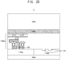
- a wafer-to-wafer bonding process may be carried out.
- a second wafer 1300 may be provided on a first surface of the first semiconductor device 1200a.
- the second wafer 1300 may be bonded by an adhesive layer 1400 provided between the first semiconductor device 1200a and the second wafer 1300.
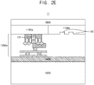
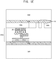
- the semiconductor architecture 11 is flipped as illustrated in FIG. 2E .
- the sacrificial layer 1600 may be removed.
- a second semiconductor device 1200b may be provided on the second surface of the carrier substrate 1100 based on the locations of the alignment marks 110 provided on the first surface of the carrier substrate 1100.
- the second semiconductor device 1200b may be an integrated circuit including components such as, for example, a TSV 130.
- the TSV 130 may be formed to penetrate the carrier substrate 1100.
- the second semiconductor device 1200b may be provided on the second surface of the carrier substrate 1100 based on the alignment marks 110.
- the TSV 130 may be misaligned with the BPR 120.
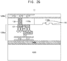
- the alignment marks 110 may include alignment marks detected by a litho-scanning method and/or alignment marks (overlay marks) detected by using an overlay tool.
- the signals provided by the alignment marks 110 from the second side of the carrier substrate 1100 may be weak due to the low depth of the alignment marks 110. Thus, accurate detection of locations of the alignment marks from the second surface of the carrier substrate 1100 may be difficult. Due to the misalignment between the first semiconductor device 1200a and the second semiconductor device 1200b, the performance of the semiconductor architecture 11 may be deteriorated.
- FIG. 3 illustrates a perspective view of a 3D heterogeneous integrated semiconductor architecture according to an example embodiment.
- the 3D heterogeneous integrated semiconductor architecture 1 may include a carrier substrate 100, a first semiconductor device 200a provided on a first surface of the carrier substrate 100, and a second semiconductor device 200b provided on a second surface of the carrier substrate 100, opposite to the first semiconductor device 200a.
- the first semiconductor device 200a and the second semiconductor device 200b may be integrated to each other and may form a 3D heterogeneous integrated semiconductor architecture 1.
- the carrier substrate 100 may include, for example, a silicon (Si) substrate, a glass substrate, a sapphire substrate, etc. However, embodiments are not limited thereto. As illustrated in FIG. 3 , the carrier substrate 100 may be a circular panel, but the shape of the carrier substrate 100 is not limited thereto. For example, the carrier substrate 100 may be a tetragonal panel. The carrier substrate 100 may include a single layer or multiple layers.
- FIG. 4 illustrates a cross-sectional view taken along line I-I' of FIG. 3 according to an example embodiment.
- the 3D heterogeneous integrated semiconductor architecture 1 may include a carrier substrate 100.
- the carrier substrate 100 includes a device area 100a and an alignment mark area 100b.
- the alignment mark area 100b includes alignment marks 10 that may be formed from the first surface of the carrier substrate 100 to the second surface of the carrier substrate 100.
- the 3D heterogeneous integrated semiconductor architecture 1 also includes a first semiconductor device 200a formed on a first surface of the carrier substrate 100 and a second semiconductor device 200b provided on a second surface of the carrier substrate 100.
- the first semiconductor device 200a may be an integrated circuit including components such as, for example, a BPR 20.
- the BPR 20 may be provided to face the first surface of the carrier substrate 100.
- the second semiconductor device 200b may be another integrated circuit and components such as, for example, a TSV 30 may protrude from the second semiconductor device 200b.
- the TSV 30 may be formed to penetrate the carrier substrate 100.
- the alignment between the BPR 20 and the TSV 30 may be improved as compared to the comparative example, and the first semiconductor device 200a and the second semiconductor device 200b may be more accurately aligned with each other as compared to the comparative example, due to improvements to the alignment marks 10 as will be discussed below.
- the integration and the performance of the semiconductor architecture 1 may be improved. Further, by providing semiconductor devices on both of the first surface of the carrier substrate 100 and the second surface of the carrier substrate 100, the size of the semiconductor architecture 1 may be reduced, and the power consumption may also be reduced.
- FIGS. 5A through 5G illustrate a method of manufacturing a 3D heterogeneous integrated semiconductor architecture 1 according to an example embodiment.
- the method includes providing a wafer including a carrier substrate 100, a stopper layer 500, and a sacrificial layer 600.
- the carrier substrate 100 may include a device area 100a and an alignment mark area 100b.
- the alignment mark area 100b may be an area of the carrier substrate 100 where the alignment marks 10 are formed.
- the carrier substrate 100 may include, for example, a silicon (Si) substrate, a glass substrate, a sapphire substrate, etc. However, materials of the carrier substrate 100 are not limited thereto.
- the carrier substrate 100 may be provided as a circular panel, but the shape of the carrier substrate 100 is not limited thereto.
- the carrier substrate 100 may be a tetragonal panel.
- the carrier substrate 100 may be provided as a single layer or multiple layers.
- the sacrificial layer 600 may include a single layer or multiple layers.
- the sacrificial layer 600 may include a polymer material, an ultraviolet (UV) film, Si, or resin.
- materials of the sacrificial layer 600 are not limited thereto. According to an example embodiment, the sacrificial layer 600 may be omitted.
- the stopper layer 500 may be, for example, a reactive-ion etching (RIE) stopper layer.
- the stopper layer 500 may be formed on one of the carrier substrate 100 and the sacrificial layer 600.
- the stopper layer 500 may be formed by epitaxial growth of a silicon germanium (SiGe) layer on the carrier substrate 100.
- SiGe silicon germanium
- the stopper layer 500 may be an oxide layer formed in a silicon-on-insulator (SOI) wafer.
- the stopper layer 500 may include silicon dioxide (SiO 2 ), Si, sapphire, etc.
- the stopper layer 500 may be a silicon nitride (SiN) layer according to another example embodiment.
- the method includes forming alignment marks 10 in the alignment mark area 100b of the carrier substrate 100 to a depth of the stopper layer 500.
- the alignment marks 10 are provided to a level of a first surface of the stopper layer 500.
- the alignment marks 10 may be formed by etching openings or trenches on a first surface of the carrier substrate 100 to a first surface of the stopper layer 500.
- the etching may include dry etching or wet etching. However, embodiments are not limited thereto.
- the second surface of the alignment marks 10 are coplanar with the first surface of the stopper layer 500.
- the uniformity of depths of the alignment marks 10 may be improved and alignment marks 10 may be formed at a deeper depth without damaging the wafer.
- the method includes providing a first semiconductor device 200a on the first surface of the carrier substrate 100 based on the detected locations of the alignment marks 10.
- the alignment marks 10 may include alignment marks detected by a litho-scanning method and overlay marks detected by using an overlay tool.
- the first semiconductor device 200a may be an integrated circuit including components such as, for example, a BPR 20.
- the BPR 20 may be provided on the first surface of the carrier substrate 100 when integrating the first semiconductor device 200a on the carrier substrate 100.
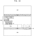
- the method may include carrying out a wafer-to-wafer bonding process.
- a second wafer 300 may be provided on a first surface of the first semiconductor device 200a.
- the second wafer 300 may be bonded to the first semiconductor device 200a by providing an adhesive layer 400 between the first semiconductor device 200a and the second wafer 300.
- the second wafer 300 may be directly provided on the first semiconductor device 200a.
- the second wafer 300 may be directly bonded to the first semiconductor device 200a by Si direct bonding without using an adhesive layer.
- the semiconductor architecture 1 may be flipped as illustrated in FIG. 5E , for second surface integration.
- the method may include removing the sacrificial layer 600 to the level of the stopper layer 500 by a grinding process.
- the grinding process may include chemical-mechanical polishing (CMP) or dry etching, but embodiments are not limited thereto.
- CMP chemical-mechanical polishing
- the stopper layer 500 may be removed.
- the stopper layer 500 may be removed by etching such as, for example, dry etching. However, embodiments are not limited thereto.
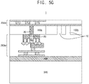
- the method includes providing a second semiconductor device 200b on the second surface of the carrier substrate 100 based on the detected locations of the alignment marks 10.
- the alignment marks 10 on the second surface of the carrier substrate 100 may include alignment marks detected based on a litho-scanning method and overlay marks detected by using an overlay tool. As the alignment marks 10 are exposed on the second surface of the carrier substrate 100, the signals provided by the alignment marks 10 in the litho-scanning method and the overlay tool may be stronger, and thus, accuracy of the detection of alignment marks 10 may be improved.
- the second semiconductor device 200b may be an integrated circuit and components such as, for example, a TSV 30 may protrude from the second semiconductor device 200b.
- the TSV 30 may be formed to penetrate through the carrier substrate 100.
- the second semiconductor device 200b may be integrated on the second surface of the carrier substrate 100 such that the TSV 30 of the second semiconductor device 200b is aligned with the BPR 20 of the first semiconductor device 200a based on the detected locations of the alignment marks 10.
- One surface of the alignment mark 10 may be coplanar with one surface of the second semiconductor device 200b.
- the overall alignment and accuracy of overlay between the BPR 20 and the TSV 30 may be improved according to an example embodiment.
- the first semiconductor device 200a and the second semiconductor device 200b may be more accurately aligned with each other.
- the integration and the performance of the semiconductor architecture 1 may be improved.
- 3D integration of semiconductor devices on both sides of the wafer may result in the reduction of size and power consumption of the semiconductor architecture 1.
- FIG. 6 illustrates a perspective view of the wafer in FIG. 5B according to an example embodiment
- the first surface of the carrier substrate 100 includes markers 12 provided in the alignment mark area 100b of the carrier substrate 100.
- each marker 12 includes a plurality of alignment marks 10.
- the alignment marks 10 may have rectangular shapes and may be provided one-dimensionally. The side surfaces of adjacent alignment marks 10 may be parallel to each other.
- the alignment marks 10 may have a width of around 8 ⁇ m and a pitch of around 16 ⁇ m.
- the shape and size of the alignment marks 10 are not limited thereto.
- the alignment marks 10 may have a cross shape.
- the alignment marks 10 may be provided two-dimensionally.
- the alignment marks 10 may have a rectangular shape and directions of the alignment marks 10 from a first plan view may be perpendicular to each other.
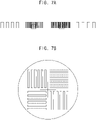
- FIGS. 7A and 7B illustrate example top plan views of markers including alignment marks in FIG. 6 according to example embodiments.
- the alignment marks 10 included in a marker 12 may have rectangular shapes and may be provided one-dimensionally.
- the alignment marks 10 may include alignment marks detected by a litho-scanning method and overlay marks detected by using an overlay tool.
- alignment marks 10 may be formed two-dimensionally in a marker 12.
- groups of a plurality of alignment marks 10 may be provided to be perpendicular to each other as illustrated in FIG. 7B .
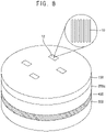
- FIG. 8 illustrates a perspective view of the semiconductor architecture 1 after removing the stopper layer 500 in FIG. 5F .
- each alignment marker 12 may include a plurality of alignment marks 10.
- the alignment marks 10 may have rectangular shapes and may be provided one-dimensionally.
- the side surfaces of adjacent alignment marks 10 may be parallel to each other.
- the alignment marks 10 may have a width of around 8 ⁇ m and a pitch of around 16 ⁇ m.
- the shape and size of the alignment marks 10 are not limited thereto.
- the alignment marks 10 may have a cross shape.
- the alignment marks 10 may be provided two-dimensionally.
- FIG. 9 illustrates a flow chart of a method of manufacturing a 3D heterogeneous integrated semiconductor architecture according to an example embodiment.
- a wafer including a carrier substrate is provided (S110).
- the carrier substrate may include a device area and an alignment mark area.
- the alignment mark area may be an area of the carrier substrate where the alignment marks are formed.
- the carrier substrate may include, for example, a silicon (Si) substrate, a glass substrate, a sapphire substrate, etc. However, materials of the carrier substrate are not limited thereto.
- the carrier substrate may be provided as a circular panel, but the shape of the carrier substrate is not limited thereto.
- the carrier substrate may be a tetragonal panel.
- the carrier substrate may be provided as a single layer or multiple layers.
- a stopper layer is formed on the carrier substrate and a sacrificial layer is formed on the stopper layer (S120).
- the stopper layer may be formed by epitaxial growth of a silicon germanium (SiGe) layer on a carrier substrate.
- the stopper layer may be an oxide layer formed in a silicon-on-insulator (SOI) wafer.
- the stopper layer may be a silicon nitride (SiN) layer.
- alignment marks are formed on a first surface of the carrier substrate to the depth of the stopper layer (S 130).
- the alignment marks may be etched in the alignment marks areas provided in the first surface of the carrier substrate.
- the alignment marks may be formed by etching openings or trenches on a first surface of the carrier substrate to the depth of the stopper layer.
- a second surface of the alignment marks and a first surface of the stopper layer may be coplanar.
- the etching may include dry etching or wet etching. However, embodiments are not limited thereto.
- the first surface of the carrier substrate may include markers provided in the alignment mark area of the carrier substrate.
- Each marker may include a plurality of alignment marks.
- the alignment marks may have rectangular shapes and may be provided one-dimensionally.
- the alignment marks may have a width of around 8 ⁇ m and a pitch of around 16 ⁇ m.
- the shape and size of the alignment marks are not limited thereto.
- the alignment marks may have a cross shape.
- the alignment marks may be provided two-dimensionally.
- a first semiconductor device is provided on a first surface of the carrier substrate based on the alignment marks (S140).
- the first semiconductor device is formed on the first surface of the carrier substrate based on locations of the alignment marks detected by, for example, litho-scanning or by using an overlay tool.
- the first semiconductor device may be an integrated circuit including components such as, for example, a BPR.
- the BPR may be provided on the first surface of the carrier substrate.
- a wafer-to-wafer bonding process is carried out (S150).
- a second wafer may be provided on a first surface of the first semiconductor device.
- the second wafer may be bonded to the first surface of the first semiconductor device by providing an adhesive layer between the second wafer and the first semiconductor device.
- the second wafer may be directly provided on the first semiconductor device through, for example, Si direct bonding, without including an adhesive layer.
- the semiconductor architecture is flipped (S160).
- the sacrificial layer is removed to the depth of the stopper layer (S170).
- the sacrificial layer may be removed by a grinding process including, for example, CMP or dry etching. However, embodiments are not limited thereto.
- the stopper layer is removed (S180).
- the stopper layer may be removed by, for example, wet etching. However, embodiments are not limited thereto.
- the alignment marks are exposed on the second surface of the carrier substrate.
- the shape and size of the alignment marks correspond to the shape and size of the alignment marks provided on the first surface of the carrier substrate.
- the alignment marks may have rectangular shapes and may be provided one-dimensionally. For example, the alignment marks may have a width of around 8 ⁇ m and a pitch of around 16 ⁇ m. However, the shape and size of the alignment marks are not limited thereto.
- the alignment marks may have a cross shape. According to another example embodiment, the alignment marks may be provided two-dimensionally
- a second semiconductor device is provided on the second surface of the carrier substrate based on the alignment marks (S190).
- the alignment marks may include alignment marks detected based on a litho-scanning method and alignment marks detected by using an overlay tool. As the alignment marks are exposed on the second surface of the carrier substrate, the signals provided by the alignment marks in the litho-scanning and the overlay tool may be stronger, and thus, accuracy of the detection of alignment marks may be improved.
- the second semiconductor device may be an integrated circuit including components such as, for example, a TSV.
- the TSV may be provided to penetrate through the carrier substrate.
- the second semiconductor device may be integrated on the second surface of the carrier substrate such that, for example, the TSV of the second semiconductor device are aligned with the BPR of the first semiconductor device based on the detected locations of the alignment marks.
- the alignment between the semiconductor devices provided on the first surface and the second surface of the wafer may become more accurate.
- the integration and the performance of the semiconductor architecture may be improved.
- 3D integration of semiconductor devices on both sides of the wafer may reduce the size and power consumption of the semiconductor architecture.
- FIG. 10 illustrates a semiconductor package that may incorporate the 3D heterogeneous integrated semiconductor architectures according to example embodiments.
- a semiconductor package 2000 may include a processor 2200 and semiconductor devices 2300 that are mounted on a substrate 2100.
- the processor 2200 and/or the semiconductor devices 2300 may include one or more of 3D heterogeneous integrated semiconductor architecture 1 described in the above example embodiments.
- FIG. 11 illustrates a schematic block diagram of an electronic system according to an example embodiment.
- an electronic system 3000 in accordance with an embodiment may include a microprocessor 3100, a memory 3200, and a user interface 3300 that perform data communication using a bus 3400.
- the microprocessor 3100 may include a central processing unit (CPU) or an application processor (AP).
- the electronic system 3000 may further include a random access memory (RAM) 3500 in direct communication with the microprocessor 3100.
- the microprocessor 3100 and/or the RAM 3500 may be implemented in a single module or architecture.
- the user interface 3300 may be used to input data to the electronic system 3000, or output data from the electronic system 3000.
- the user interface 3300 may include a keyboard, a touch pad, a touch screen, a mouse, a scanner, a voice detector, a liquid crystal display (LCD), a micro light-emitting device (LED), an organic light-emitting diode (OLED) device, an active-matrix light-emitting diode (AMOLED) device, a printer, a lighting, or various other input/output devices without limitation.
- the memory 3200 may store operational codes of the microprocessor 3100, data processed by the microprocessor 3100, or data received from an external device.
- the memory 3200 may include a memory controller, a hard disk, or a solid state drive (SSD).
- At least the microprocessor 3100, the memory 3200 and/or the RAM 3500 in the electronic system 3000 may include a 3D heterogeneous integrated semiconductor architecture 1 as described in the above example embodiments.
Landscapes
- Engineering & Computer Science (AREA)
- Power Engineering (AREA)
- Microelectronics & Electronic Packaging (AREA)
- Computer Hardware Design (AREA)
- Physics & Mathematics (AREA)
- General Physics & Mathematics (AREA)
- Condensed Matter Physics & Semiconductors (AREA)
- Manufacturing & Machinery (AREA)
- Geometry (AREA)
- Container, Conveyance, Adherence, Positioning, Of Wafer (AREA)
Applications Claiming Priority (2)
| Application Number | Priority Date | Filing Date | Title |
|---|---|---|---|
| US202063113626P | 2020-11-13 | 2020-11-13 | |
| US17/157,374 US11694968B2 (en) | 2020-11-13 | 2021-01-25 | Three dimensional integrated semiconductor architecture having alignment marks provided in a carrier substrate |
Publications (1)
| Publication Number | Publication Date |
|---|---|
| EP4002439A1 true EP4002439A1 (en) | 2022-05-25 |
Family
ID=78528699
Family Applications (1)
| Application Number | Title | Priority Date | Filing Date |
|---|---|---|---|
| EP21206428.1A Pending EP4002439A1 (en) | 2020-11-13 | 2021-11-04 | Three dimensional integrated semiconductor architecture and method of manufacturing the same |
Country Status (5)
| Country | Link |
|---|---|
| US (2) | US11694968B2 (zh) |
| EP (1) | EP4002439A1 (zh) |
| KR (1) | KR20220065662A (zh) |
| CN (1) | CN114496992A (zh) |
| TW (1) | TW202220164A (zh) |
Families Citing this family (1)
| Publication number | Priority date | Publication date | Assignee | Title |
|---|---|---|---|---|
| US20220336355A1 (en) * | 2021-04-19 | 2022-10-20 | Samsung Electronics Co., Ltd. | Thermal budget enhanced buried power rail and method of manufacturing the same |
Citations (6)
| Publication number | Priority date | Publication date | Assignee | Title |
|---|---|---|---|---|
| US20080179678A1 (en) * | 2007-01-26 | 2008-07-31 | International Business Machines Corporation | Two-sided semiconductor-on-insulator structures and methods of manufacturing the same |
| US20090225331A1 (en) * | 2008-03-04 | 2009-09-10 | Asml Netherlands B.V. | Method of Providing Alignment Marks, Device Manufacturing Method and Lithographic Apparatus |
| US20130214337A1 (en) * | 2012-02-17 | 2013-08-22 | Renesas Electronics Corporation | Semiconductor device and manufacturing method thereof |
| US20170176871A1 (en) * | 2014-02-21 | 2017-06-22 | Asml Netherlands B.V. | Optimization of target arrangement and associated target |
| EP3324436A1 (en) * | 2016-11-21 | 2018-05-23 | IMEC vzw | An integrated circuit chip with power delivery network on the backside of the chip |
| US20200098737A1 (en) * | 2018-09-25 | 2020-03-26 | Intel Corporation | Stacked-substrate fpga semiconductor devices |
Family Cites Families (22)
| Publication number | Priority date | Publication date | Assignee | Title |
|---|---|---|---|---|
| US6372600B1 (en) | 1999-08-30 | 2002-04-16 | Agere Systems Guardian Corp. | Etch stops and alignment marks for bonded wafers |
| JP2003203852A (ja) | 2002-01-09 | 2003-07-18 | Mitsubishi Electric Corp | アライメントマーク構造およびその製造方法、アライメントマーク検出方法 |
| JP4342202B2 (ja) | 2003-04-14 | 2009-10-14 | Okiセミコンダクタ株式会社 | アライメントマークの形成方法およびそれを用いた半導体装置の製造方法 |
| US8299583B2 (en) * | 2009-03-05 | 2012-10-30 | International Business Machines Corporation | Two-sided semiconductor structure |
| US8264065B2 (en) * | 2009-10-23 | 2012-09-11 | Synopsys, Inc. | ESD/antenna diodes for through-silicon vias |
| US20110177435A1 (en) * | 2010-01-20 | 2011-07-21 | International Business Machines Corporation | Photomasks having sub-lithographic features to prevent undesired wafer patterning |
| US8896136B2 (en) * | 2010-06-30 | 2014-11-25 | Taiwan Semiconductor Manufacturing Company, Ltd. | Alignment mark and method of formation |
| US8928159B2 (en) * | 2010-09-02 | 2015-01-06 | Taiwan Semiconductor Manufacturing & Company, Ltd. | Alignment marks in substrate having through-substrate via (TSV) |
| US20190363001A1 (en) * | 2010-11-18 | 2019-11-28 | Monolithic 3D Inc. | 3d semiconductor memory device and structure |
| US8546961B2 (en) | 2011-01-10 | 2013-10-01 | International Business Machines Corporation | Alignment marks to enable 3D integration |
| US8563396B2 (en) | 2011-01-29 | 2013-10-22 | International Business Machines Corporation | 3D integration method using SOI substrates and structures produced thereby |
| US20120193785A1 (en) * | 2011-02-01 | 2012-08-02 | Megica Corporation | Multichip Packages |
| JP2012164702A (ja) * | 2011-02-03 | 2012-08-30 | Elpida Memory Inc | 半導体装置 |
| JP2012178520A (ja) * | 2011-02-28 | 2012-09-13 | Elpida Memory Inc | 半導体装置及びその製造方法 |
| JP5275400B2 (ja) * | 2011-04-18 | 2013-08-28 | 新光電気工業株式会社 | 配線基板、半導体装置及び配線基板の製造方法 |
| CN103050480B (zh) | 2012-08-14 | 2015-08-19 | 上海华虹宏力半导体制造有限公司 | 硅片的背面图形化的工艺方法 |
| US8957504B2 (en) * | 2013-03-15 | 2015-02-17 | IP Enval Consultant Inc. | Integrated structure with a silicon-through via |
| US9184041B2 (en) * | 2013-06-25 | 2015-11-10 | Taiwan Semiconductor Manufacturing Co., Ltd. | Integrated circuit with backside structures to reduce substrate warp |
| US10014292B2 (en) * | 2015-03-09 | 2018-07-03 | Monolithic 3D Inc. | 3D semiconductor device and structure |
| US9570395B1 (en) * | 2015-11-17 | 2017-02-14 | Samsung Electronics Co., Ltd. | Semiconductor device having buried power rail |
| US20190123035A1 (en) | 2017-10-19 | 2019-04-25 | Samsung Electronics Co., Ltd. | Method of performing die-based heterogeneous integration and devices including integrated dies |
| US11227812B2 (en) * | 2019-08-28 | 2022-01-18 | Taiwan Semiconductor Manufacturing Company, Ltd. | Package and manufacturing method thereof |
-
2021
- 2021-01-25 US US17/157,374 patent/US11694968B2/en active Active
- 2021-09-23 KR KR1020210125558A patent/KR20220065662A/ko unknown
- 2021-11-04 EP EP21206428.1A patent/EP4002439A1/en active Pending
- 2021-11-09 TW TW110141615A patent/TW202220164A/zh unknown
- 2021-11-11 CN CN202111331491.4A patent/CN114496992A/zh active Pending
-
2023
- 2023-05-18 US US18/319,765 patent/US20230290734A1/en active Pending
Patent Citations (6)
| Publication number | Priority date | Publication date | Assignee | Title |
|---|---|---|---|---|
| US20080179678A1 (en) * | 2007-01-26 | 2008-07-31 | International Business Machines Corporation | Two-sided semiconductor-on-insulator structures and methods of manufacturing the same |
| US20090225331A1 (en) * | 2008-03-04 | 2009-09-10 | Asml Netherlands B.V. | Method of Providing Alignment Marks, Device Manufacturing Method and Lithographic Apparatus |
| US20130214337A1 (en) * | 2012-02-17 | 2013-08-22 | Renesas Electronics Corporation | Semiconductor device and manufacturing method thereof |
| US20170176871A1 (en) * | 2014-02-21 | 2017-06-22 | Asml Netherlands B.V. | Optimization of target arrangement and associated target |
| EP3324436A1 (en) * | 2016-11-21 | 2018-05-23 | IMEC vzw | An integrated circuit chip with power delivery network on the backside of the chip |
| US20200098737A1 (en) * | 2018-09-25 | 2020-03-26 | Intel Corporation | Stacked-substrate fpga semiconductor devices |
Also Published As
| Publication number | Publication date |
|---|---|
| KR20220065662A (ko) | 2022-05-20 |
| US11694968B2 (en) | 2023-07-04 |
| TW202220164A (zh) | 2022-05-16 |
| US20230290734A1 (en) | 2023-09-14 |
| US20220157737A1 (en) | 2022-05-19 |
| CN114496992A (zh) | 2022-05-13 |
Similar Documents
| Publication | Publication Date | Title |
|---|---|---|
| US20180019139A1 (en) | Wafer-Level Etching Methods for Planar Photonics Circuits and Devices | |
| EP4002435A1 (en) | Semiconductor device with backside power distribution network and method of manufacturing the same | |
| US6420266B1 (en) | Methods for creating elements of predetermined shape and apparatuses using these elements | |
| US9773702B2 (en) | Device without zero mark layer | |
| US20230290734A1 (en) | Three dimensional integrated semiconductorarchitecture having alignment marks provided in a carrier substrate | |
| CN105702626A (zh) | 制造半导体芯片的方法以及定位切割部件的方法 | |
| US11728324B2 (en) | Semiconductor structure having photonic die and electronic die | |
| US9269607B2 (en) | Wafer stress control with backside patterning | |
| US20130149836A1 (en) | Method of double-sided patterning | |
| KR20230037608A (ko) | 정렬 마크를 구비한 웨이퍼 어셈블리 및 이의 형성 방법, 웨이퍼 정렬 방법 | |
| US8772136B2 (en) | Method for fabricating semiconductor device | |
| CN115763237A (zh) | 晶圆切割方法 | |
| US9105644B2 (en) | Apparatus and method for forming alignment features for back side processing of a wafer | |
| KR100558201B1 (ko) | 포토 정렬키 및 포토 정렬키를 포함하는 반도체 소자 제조방법 | |
| EP3660902A1 (en) | Semiconductor device comprising an aperture array | |
| JP2010016150A (ja) | 半導体装置の製造方法 | |
| US20230154914A1 (en) | Method of producing hybrid semiconductor wafer | |
| TW202410265A (zh) | 平面光子電路及裝置用之晶圓級蝕刻方法 | |
| KR20200113519A (ko) | Soi 제조 방법 | |
| TW202418381A (zh) | 半導體元件、半導體支撐結構、以及半導體基底的製造方法 | |
| CN117832194A (zh) | 半导体装置及其制造方法 | |
| CN115863366A (zh) | 一种浅沟槽对准图形形成方法及半导体器件 | |
| CN116759335A (zh) | 键合装置、键合装置的形成方法及键合方法 | |
| KR20090077539A (ko) | 반도체 집적 회로 장치 및 그 제조 방법 |
Legal Events
| Date | Code | Title | Description |
|---|---|---|---|
| PUAI | Public reference made under article 153(3) epc to a published international application that has entered the european phase |
Free format text: ORIGINAL CODE: 0009012 |
|
| STAA | Information on the status of an ep patent application or granted ep patent |
Free format text: STATUS: THE APPLICATION HAS BEEN PUBLISHED |
|
| STAA | Information on the status of an ep patent application or granted ep patent |
Free format text: STATUS: REQUEST FOR EXAMINATION WAS MADE |
|
| AK | Designated contracting states |
Kind code of ref document: A1 Designated state(s): AL AT BE BG CH CY CZ DE DK EE ES FI FR GB GR HR HU IE IS IT LI LT LU LV MC MK MT NL NO PL PT RO RS SE SI SK SM TR |
|
| 17P | Request for examination filed |
Effective date: 20220516 |
|
| RBV | Designated contracting states (corrected) |
Designated state(s): AL AT BE BG CH CY CZ DE DK EE ES FI FR GB GR HR HU IE IS IT LI LT LU LV MC MK MT NL NO PL PT RO RS SE SI SK SM TR |
|
| P01 | Opt-out of the competence of the unified patent court (upc) registered |
Effective date: 20230520 |